| Journal of Renewable Materials |
DOI: 10.32604/jrm.2023.022773
REVIEW
Fabrication and Modification Strategies of Metal Halide Perovskite Absorbers
Experimental Centre for Advanced Materials, School of Materials Science and Engineering, Beijing Institute of Technology, Beijing, 100081, China
*Corresponding Authors: Yang Bai. Email: mse.ybai@bit.edu.cn; Qi Chen. Email: qic@bit.edu.cn
Received: 26 March 2022; Accepted: 16 May 2022
Abstract: Due to the long carrier lifetime, high carrier mobility, and high absorption coefficient of perovskite materials, the power conversion efficiency (PCE) of perovskite solar cells (PSCs) has increased from 3.8% in 2009 to 25.7% in 2021, which have already surpassed the PCE of thin-film solar cells and closes to the efficiency of Si-based photovoltaics (26.7%). Therefore, PSCs have become a promising clean energy technology for commercialization. However, the low defect formation energy of perovskite leads to a higher defect density than other conventional photovoltaic materials. It results in severe non-radiative recombination, limiting its further development and the commercialization. In this review, we summarize the mechanism and strategies for high-quality perovskite absorber fabrications to minimize the bulk and surface/interface defects of halide perovskite, including film quality development and interface modification. Strategies are proposed for further promoting the film quality and the corresponding device performance. Finally, we highlight the challenges that need to be overcome to control over the defect properties of halide perovskite.
Keywords: Perovskite; defect; interface modification; film quality; passivation
Metal halide perovskite materials have attracted tremendous attention due to their unique feature as long carrier lifetime, high carrier mobility, and large absorption coefficient [1–7]. The PCE of perovskite solar cells shows dramatic increases from 3.8% in 2009 to 25.7% in 2021, surpassing that of the dye-sensitized solar cells (13.2%), organic solar cells (17.4%), copper indium gallium selenide solar cells (23.4%) and cadmium telluride thin-film technologies (22.1%), and closing to the single crystal gallium arsenide cells (27.8%) and Si-based photovoltaics (26.7%) (Fig. 1) [8]. The fast development and high efficiency make it a promising clean energy technology for commercialization [9]. In addition, although the highest certified efficiency of PSCs has reached 25.7%, the PCE reported in the current paper is still around 22%∼24%, and it is estimated that the average PCE in the laboratory may be less than 23%, which limits the commercialization of PSCs.

Figure 1: The National Renewable Energy Laboratory (NREL) solar cell efficiency chart [8]
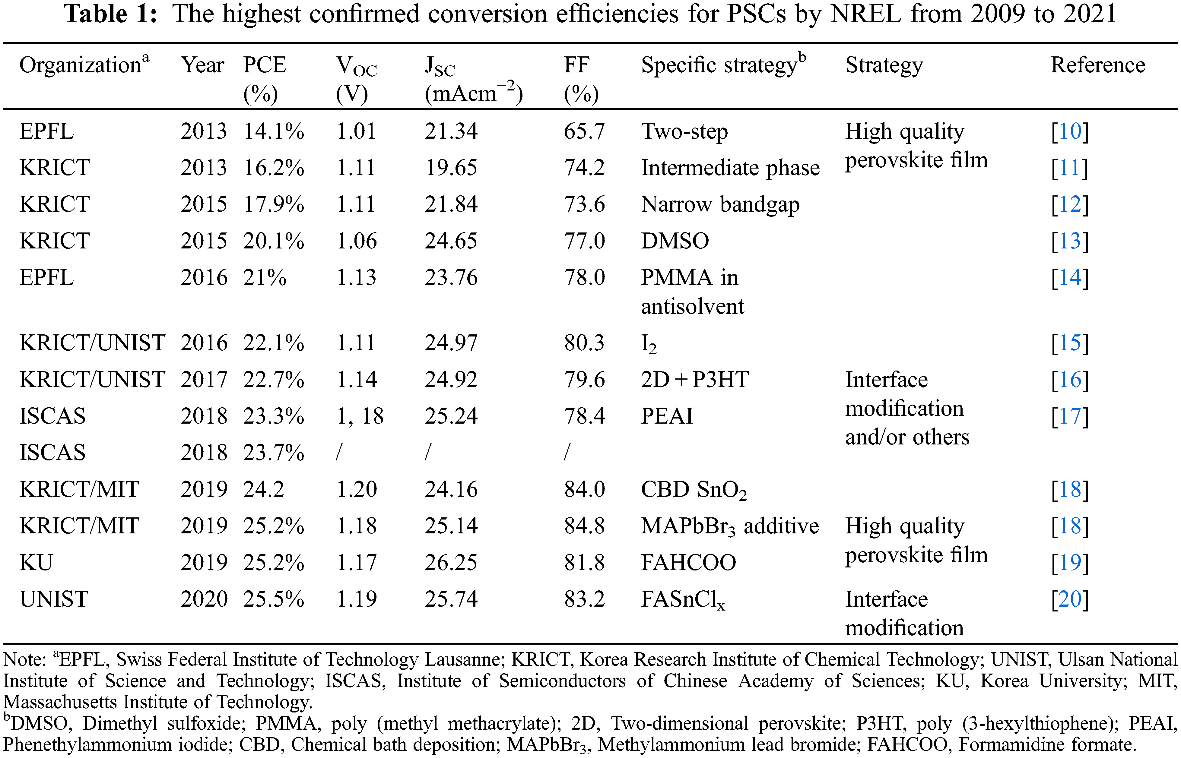
High defect density is one of the major reasons that limit the development of PSCs efficiency. Compared with silicon, perovskite has a suitable optical band gap, shallow defect, high light absorption coefficient, and direct bandgap, presenting suitable features for photovoltaic technology. However, the defect formation energy of perovskite materials is low, resulting in a higher defect density (>1015 cm−3) than that of crystalline Si (∼1010 cm−3). High defect density leads to a severe non-radiative recombination, which further limits the open-circuit voltage (VOC) and fill factor (FF) of PSC devices. Therefore, fabricating high-quality perovskite film and modifying the surface/boundaries to reduce the defects in bulk and at surface are the keys to improving the PCE of PSCs (Table 1).
2 Fabrication of High-Quality Perovskite Films
For photovoltaic application, a material should have the high absorption coefficient, which can also harvest the photons and convert them into charge carriers efficiently. However, in PSCs, the photon-harvesting and carrier generation processes are accompanied by carrier recombination, which competes with carrier transfer, leading to performance reduction. Recombination losses are inevitable in solar cells, and there are three basic types of recombination: radiative recombination, defect-assisted recombination, and Auger recombination [21,22]. The whole recombination process can be described as:
where n is the photo-generated carrier density, and
The defects of perovskite film are broadly classified as bulk defects (such as grain boundary or impurities) and surface/interface defects. Improving the film quality to reduce the bulk defect is crucial to enhancing the performance of perovskite devices. Ideally, a single crystal perovskite film can be formed on the substrate to minimize the defect density. However, the method for preparing high-efficiency single-crystal perovskite solar cells is still challenging. Recently, research for PSCs development still focuses on polycrystalline perovskite films.
2.1 Mechanism of Perovskite Film Formation
Nucleation is important for controlling the film quality in the solution method, which determines the property of the subsequent growth process and ultimately determines the properties of the crystalline film. The nucleation and growth of perovskite films are simultaneous in the preparation process.
When the solution is saturated, nucleating phases will aggregate together to form a small crystal nucleus, such as formula units, atoms, ions, and molecules (Fig. 2A). Driven by the thermodynamic principle, nucleation occurs at the base/precursor/solution interfaces or in the precursor solution when the volume free energy of the solid phase is lower than that of the liquid phase [23,24]. According to the nucleation site, nucleation can be divided into heterogeneous and homogeneous nuclei.

Figure 2: (A) The schematic of the La Mer diagram for homogeneous nucleation. CS is the solubility, CSmin is the supersaturation limit (the minimum concentration for nucleation), and CSmax is the critical supersaturation limit (the maximum concentration for nucleation). The regions I, II, and III represent solution, nucleation, and growth, respectively. (B) Schematic diagram of the classical free energy (ΔG) diagram for homogeneous nucleation as a function of particle radius (r). ΔGS is the surface free energy, and ΔGV is the bulk free energy. ΔGC is critical free energy, and rC is the critical radius of the nucleus. Adapted from Lee et al. [24] with permission from Wiley, Copyright 2018
The saturation of the precursor is the driving force of perovskite nucleation. For the homogeneous nucleation, the total free-energy change (ΔG) is the sum of surface free energy and volume free energy, which is a function of nucleus radius (r):
where V and A are the nucleus volume and surface area, respectively. ΔGV and γCL is the volume and interface energy change between the liquid (L) and the crystalline (C) nucleus, respectively.
The V and A are related to nucleus radius (r), and ΔGV is determined by the saturation:
where VM is the molar volume of the nucleus, R is the gas constant, and T is the Kelvin temperature. S is the saturation ratio, which is equal to C/CS. Where C is the solute concentration in the precursor solution and CS is the equilibrium solubility limit. The ΔG of homogeneous nucleation is plotted schematically in Fig. 2B, which first increases and then decreases as radius r increases. The maximum ΔGC occurs at the critical nucleus radius (rC). When the nuclei radii r < rC, nuclei tend to dissolve in solution. When the nuclei radii r > rC, the nuclei tend to grow to form the grains.
Perovskites also nucleate at interfaces during the spin coating process (heterogeneous nucleation), such as the substrate surface. And the free energy change of heterogeneous is related to the ΔGhomo and the contact angle (θ):
2.2 Strategy of Fabricating High-Quality Perovskite Film
2.2.1 Solution-Process Deposition Methods
Perovskites feature an easy and solution processability, which benefits the achieving of the efficient device under a low-temperature process. Two kinds of methods have been widely used and developed in perovskite manufacture. The one-step method, where the precursors are deposited simultaneously on the substrate, and the two-step, where the precursors are deposited sequentially on the substrate, make the synthesis of perovskite highly tunable, especially for its composition. However, with low formation energy, the perovskites exhibit fast crystallization (within a few seconds) during this solution processing, limiting the control of crystallization and growth orientation of the perovskite films [25]. So, developing suitable solution-process deposition methods with controllable nucleation and crystallization is crucial for achieving high-quality perovskite film.
One-Step Method
Kojima et al. first proposed the one-step fabrication process in 2009 [26]. In the beginning, the one-step method met many challenges for high-efficiency device fabrication, such as the poor coverage of perovskite layers on the substrate and the irregular grain orientation. And it was difficult to control the nucleation and growth of perovskite, needle-like structures and irregular rods were often observed in traditional N,N-Dimethylformamide (DMF) solvent system [27]. Due to the high boiling point of DMF solvent, the perovskite experienced a slow nucleation and growth process, leading to poor coverage. Vacuum treatment, antisolvent extraction method, substrate heating, and gas blowing methods have been developed for rapid fast solvent removal and have achieved promising encouraging results.
The introduction of the antisolvent extraction process greatly promotes the utilization of the one-step method, which was first proposed by Xiao et al. [28]. Antisolvent can reduce the solubility of perovskite in the precursor solution, which benefits solvent removal and facilitates uniform nucleation. Typically, a DMF solution of MAPbI3 was spin-coated on a substrate, and then immediately exposed to the chlorobenzene (CB) for fast crystallization (Fig. 3A). Through this strategy, PSCs yielded an average PCE of 13.9 ± 0.7% and a steady-state efficiency of 13%. Furthermore, a mixed solvent system of γ-butyrolactone (GBL) and DMSO was used to fabricate uniform and dense perovskite film via an MAI-PbI2-DMSO intermediate phase, which retarded the quick reaction between MAI and PbI2 during the spin-coating process (Figs. 3B and 3C). And the PCE was further promoted to a remarkable value of 16.2% (certified) without hysteresis [27]. So far, several antisolvents have been investigated and achieved impressive results, including hexane, diethyl ether, ethyl acetate, and toluene (Table 2) [11,28–31].

Figure 3: (A) Schematic illustration of the fast crystallization-deposition process for fabricating perovskite films. A second solvent (e.g., chlorobenzene) introduced on top of the wet film during the spin-coating process induces fast crystallization of uniformly sized perovskite grains. Adapted from Im et al. [25] with permission from Wiley, Copyright 2014. (B) Solvent engineering procedure for preparing the uniform and dense perovskite film. (C) Scheme for the formation of the perovskite material via the MAI–PbI2–DMSO intermediate phase. (i) PbI2 consists of edge-sharing [PbI6]4−octahedral layers. (ii) MAI and DMSO guest molecules intercalated between the layers, forming the flat MAI–PbI2–DMSO intermediate phase film, when toluene is introduced onto the wet film comprising PbI2, MAI, and DMSO. Here, the positions of the guest molecules are unconfirmed. (iii) Finally, the intermediate phase film is converted to the perovskite phase with corner-sharing octahedra via the extraction of DMSO guest molecules by the annealing process. The perovskite film is extremely uniform and flat because of the solid-state conversion from the uniform and flat intermediate phase film. Adapted from Im et al. [25] with permission from Nature, Copyright 2014

Two-Step Method
The two-step method is a sequential deposition method, involving (a) the nucleation and growth of deposited PbI2, (b) intercalation of cations and structural reorganization to form perovskite, and (c) the Ostwald Ripening process, in which the smaller crystals dissolve back in the solution and then deposit on larger crystals from this saturated solution, making them grow at the expense of the smaller crystals, making small crystals grow into large crystals (Fig. 4) [41]. Compared to the one-step process, the two-step process retarded the reaction between the organic and PbI2, which provided excess time to control the crystallization and the growth of the perovskite absorber.

Figure 4: Schematic depicting the stages of the reaction in the sequential deposition. Dashed arrows indicate mass transfer. (A) Nucleation and growth of PbI2. (B) Intercalation of MAI and structural reorganization to form MAPbI3 perovskite. (C) Ostwald ripening, in which the perovskite from the mesoporous layer is transported to the capping layer. (D) Further Ostwald ripening at longer dipping times in which the perovskite from the small crystals in the capping layer is transported to larger crystals. (E) Gibbs free energy as a function of the reaction coordinate. Adapted from Ummadisingu et al. [41] with permission from Science, Copyright 2018
In the case of MAPbI3, the reaction between PbI2 and MAI can be presented as [42]:
where s and soln represent solid and solution, respectively. According to this process, the film quality prepared by the two-step method can be modulated by regulating the PbI2 and cation, and the diffusion between them. The concentration of MAI could influence the cuboid MAPbI3 size. As the concentration of MAI increased, the average size of perovskite decreased, which is about 90 nm for 0.063 mmol/L, 130 nm for 0.063 mol/L, 190 nm for 0.050 mmol/L, 360 nm for 0.044 mmol/L, and 720 nm for 0.038 mmol/L. Besides, it has a critical impact on the conversion of PbI2 to perovskite. Surprisingly, the amount of residual PbI2 increases with the rising of the MAI concentration due to a non-classical perovskite ripening model in the two-step process [43]. Furthermore, the loading time of MAI on the PbI2 thin film also determined the conversion reaction of PbI2 to MAPbI3 perovskite and its corresponding photovoltaic performance. By optimizing the MAI loading time, a hysteresis-free PSCs device was achieved with a PCE of 15.58% [44].
The intramolecular exchange process (IEP) is also a key technology to prepare high-quality perovskite thin films in the two-step method. Seok et al. introduced DMSO molecules into PbI2 precursors to facilitate the spin-coating of FAI. For the conventional two-step method, the cation is inserted into the PbI2 skeleton, which may cause considerable volume expansion. This conjecture was confirmed by the alpha-step IQ surface profiler, and the thickness of the film increases from 290 to 570 nm after the reaction between PbI2 and FAI. In contrast, in the IEP method, the volume expansion was avoided (Table 3) [13]. By using the IEP film preparation technique, the PCE of FAPbI3 PSCs reached over 20% (20.1% certified efficiency). Furthermore, the IEP method was applied to mixed perovskite and achieved significant success (Table 2).

Additive engineering is commonly used to prepare high-quality thin films. The additives can reduce nucleation sites and increase the grain growth rates to prepare uniform, high quality, and dense perovskite films [11,45].
Various additives have been used for PSCs, such as organic molecules, polymers, salts, etc. [14,46–49]. Pb2+ and I− in halide perovskites can be treated as Lewis acid and Lewis base, and these features provide an almost endless space additives selection. Typically, organic molecules and polymers with groups of carbonyl, carboxyl, and/or amino can coordinate with Pb and I, or have strong interaction with the Pb-I framework. Anions and cations in organic/inorganic salts could participate in the nucleation of perovskite by modulating the nucleation process and/or the formation of nucleation sites.
Solvents additives are widely used for modulating the colloid distribution in precursors. Gamma-butyrolactone (GBL), DMF, DMSO, and/or acetonitrile (ACN) are commonly used solvents to control the colloidal clusters in the precursor [50,51]. In addition, acidic additives, such as hydroiodic (HI) and hydrobromic acids (HBr), have been used to modulate the dissolution of large size colloidal particles in perovskite precursors, resulting in increased crystallinity, grain size, and texture of perovskite [52,53]. However, the content of additives should be precisely controlled. If the concentration of additives is too high, pinholes formed in the perovskite film due to the reduction of nucleation sites, which are insufficient for the fusion of individual grains to form well-covered grains.
The polymer can also apply to modulate the crystal growth by serving as a heterogeneous nucleation site. PMMA was used as a template to control nucleation and crystal growth. Through introducing PMMA in a chlorobenzene/toluene mixture, efficient and stable PSCs were realized with an extraordinary PCE of 21.6% (21.02% certified efficiency) [14]. Silk fibroin (SF), a highly ordered β-sheets component, could interact with perovskite intermediates and worked as the crystal growth template and trap passivation agent [54]. The SF incorporated perovskites exhibited a 1000 times higher carrier mobility than the pristine perovskite with an improved PCE from 18.04% to 19.6%. Monoamine Cu porphyrin with large π-backbones was used to boost the charge carrier in polycrystalline perovskite films, thus enabling the fabrication of efficient (24.2%) and stable perovskite solar cells [55]. Other polymers, such as L-α-phosphatidylcholine, have been demonstrated to retard the crystallization rate and improve the film quality of perovskite [56,57].
In addition to molecules and polymers, other kinds of additives have also been applied for improving the film quality of the perovskite absorber. Methylammonium chloride (MACl) additive is one of the most widely used compositional additives, which tunes the crystallization process of perovskite by introducing an intermediate. Adding MACl into the precursor solution can form a chloride-rich perovskite, such as MAPbCl3, preventing the direct and uncontrol formation of iodide perovskite [58–60]. The chloride-rich perovskite can be used as a template for crystallization of iodine-based perovskite and then the chloride will eventually volatilize from the film upon annealing [61–64]. The FAPbI3 device was produced by adding the MACl additive into the antisolvent, which increased the grain size from 250 to 1500 nm and achieved a remarkable efficiency of 24.02% (23.48% certified efficiency) [65]. However, the MACl volatilizes quickly upon thermal annealing, leading to the formation of pinholes and defects in the perovskite films. By introducing extra PbCl2 to the perovskite precursor, the fast volatilization of MACl could be suppressed, resulting in a compact and pinhole-free perovskite film with large grains [66].
In addition to MACl, other chlorides were also used for PSCs toward high efficiency. NH4Cl was used to regulate the perovskite crystallization and form high crystalline perovskite films, which results in an improved PCE with a remarkably enhanced fill factor of 80.11% [67]. Guanidinium chloride (GuHCl) was also introduced to improve the MAPbI3 perovskite film quality, leading to an improved PCE of 14.20% for the HTL free PSCs [68]. By applying the ethylammonium chloride (EACl) as an additive, a PCE of 20.9% was obtained owing to the increasing crystalline grain size of perovskite film. Strontium chloride (SrCl2) was applied in a printable, HTL-free perovskite device, which increased the crystallinity and minimized the defect density, thus resulting in a remarkable improvement of PCE to 15.9% with a high VOC of 1.05 V [69]. Recently, methylenediammonium dichloride (MDACl2) was used to stabilize the α-FAPbI3 phase, achieving a certified PCE of 23.7% with a remarkable JSC of between 26.1 and 26.7 mA cm−2 [39]. Furthermore, cesium (Cs) was introduced to reduce the lattice strain in conjunction with MDACl2, resulting in a longer carrier lifetime and lower defect concentration. Benefiting from the Cs and MDACl2 doping, the PCE of PSCs was further improved to over 25% (24.4% certified efficiency) [40]. Moreover, metallic cation additives, such as K+, Sn2+, Al3+and Ag+, and ammonium halide additives, such as NH4I, butylammonium iodide (BAI) and dimethylammonium iodide (DMAI), can also be applied to modulate the nucleation to improve the perovskite film quality [70–77].
The qualities of interfaces also play a crucial role in device performance. As the terminal of the three-dimensional periodic arrangement of perovskite (Fig. 5) [78], interfaces always hold a high defect density. In the view of electronic structure, a lot of deep-level defects are located on the surface, which are the sites for the nonradiative recombination of carriers. Severe surface recombination results in low VOC and FF, and therefore, decreases the device performance. Interfacial modification for passivating defects is an essential technique for high-efficiency device fabrication.
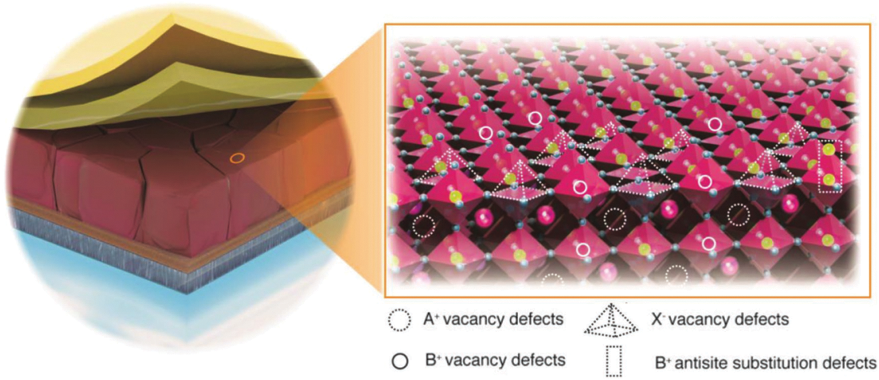
Figure 5: Schematic illustration of typical PSCs and detailed view of possible surface defects on perovskite crystals, e.g., interstitials, substitutional, and vacancies. Adapted from Aydin et al. [78] with permission from Wiley, Copyright 2019
3.1 Mechanism of Interfacial Modification
Various kinds of defects are existed on the perovskite surface, including the nonstoichiometric defects, dangling bonds, etc. (Fig. 5). The Lewis concept plays an important role in guiding defect passivation, and the Lewis acid or base molecules could passivate the defects by forming a covalent bond. For example, defects lone pairs of electrons, such as free iodide ions and lead iodine antisite defects, could be passivated by Lewis acid molecules. In contrast, the defects with deficient electrons such as Pb2+ interstitials could be passivated by Lewis base molecules. Benefiting from the passivation, deep-level trap defects could be eliminated and the device performance can be significantly improved.
3.2 Strategy of Interface Modification
Alkylammonium halides are the representative components that are being used for interface passivation, which can passivate defects via hydrogen bonding, ionic bonding, and/or coordinate bonding.
Most of the alkylammonium halides, such as phenethylammonium halide (PEAX), ethylammonium halide (EAX), guanidine halide (GUAX), n-butylammonium halide (BAX), and isobutylammonium halide (iso-BAX), could form low-dimensional (2D-0D) perovskite at the film interface/surface, thus passivating the surface defect and preventing the nonradiative recombination [69,79,80]. In addition, establishing 2D perovskite on the 3D perovskite surface could form a double-layered halide perovskite architecture, where a wide-bandgap halide (WBH) is stacked onto a narrow-bandgap halide (NBH) light absorber (Fig. 6A). This architecture optimized the interfacial contact and modulated the carrier transport between perovskite and the transporting layer [16]. For example, the n-hexyl trimethylammonium bromide (HTAB) can form the wide-bandgap layer on the perovskite and achieve a PCE of 23.3% (Fig. 6B).
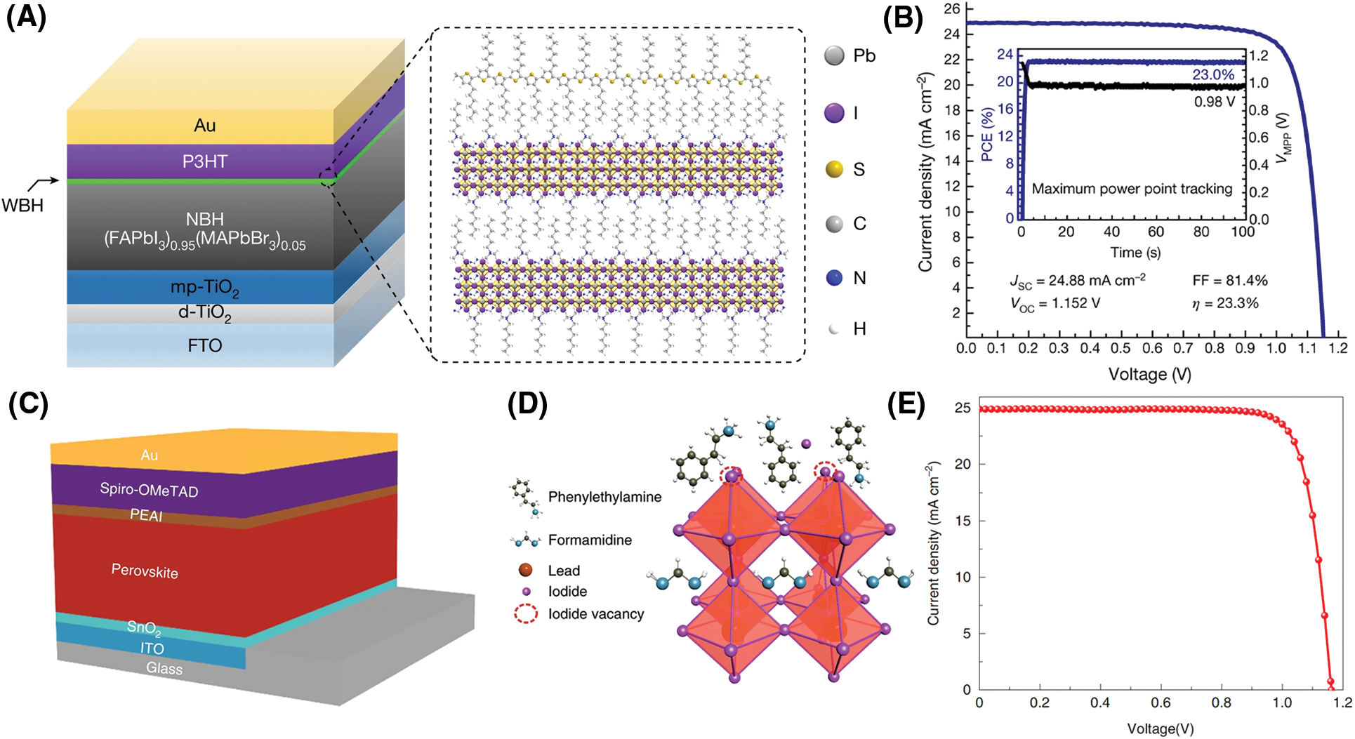
Figure 6: (A) Left, the structure of an n-i-p perovskite solar cell based on a DHA using P3HT as the hole-transport material. Right, schematic structure of the interface between the WBH and P3HT. (B) Current density–voltage (J−V) curves of the best-performing DHA-based perovskite solar cell using P3HT. The inset shows the stabilized performance measured by maximum power point tracking of the device under AM 1.5 G illumination. Adapted from Jung et al. [16] with permission from Nature, Copyright 2019. (C) The device structure was adopted in this study. PEAI is used for post-treatment of the perovskite surface. (D) Possible passivation mechanism of the PEAI layer for the perovskite film. (E) The best device we achieved in our laboratory was by optimizing the PEAI condition (20 mM). A 23.56% PCE is achieved with a VOC of 1.16 V, JSC of 24.9 mA cm−2, and FF of 81.4%. Adapted from Jiang et al. [17] with permission from Nature, Copyright 2019
Recently, studies have shown that some alkylammonium halides can directly passivate defects without forming 2D perovskite [17]. Phenethylammonium iodide (PEAI) was used to passivate surface defects and the best device PCE (23.32% certificated efficiency) was achieved without annealing (Figs. 6C–6E). PL measurement confirms that the PEAI exhibited a better passivation effect for the perovskite layer than forming a 2D perovskite (i.e., PEA2PbI4) capping layer [17]. 5-AVAI (5-ammoniumvaleric acid) was deposited on the (FAPbI3)0.88(CsPbBr3)0.12 surface, which could react with the excess PbI2 and formed the 2D (5-AVA)2PbI4 perovskite. The 2D/3D heterostructure at the perovskite/hole transport layer interface promoted carrier extraction, increasing the VOC from 0.98 to 1.07 V and the PCE from 13.7% to 16.8% [81]. 2-aminoethanethiol hydrochloride (2-AET·HCl) was spin-coated onto the halide perovskite surface to form the chemically stable Dion-Jacobson 2D perovskite, which passivated the surface defects and facilitated the interfacial charge transfer. The resulting perovskite devices exhibited a PCE > 23.5% with a high open-circuit voltage of 1.15 V [82].
In addition to alkylammonium halides, fullerene (C60) and its derivatives (e.g., PCBM, PC70BM) are also applied for surface passivation, which can accept electrons from the PbI3− antisite defects or under-coordinated halide ions, as a Lewis acid. With a thin layer of PCBM deposited on the perovskite surface, the PSCs showed a significantly enhanced PCE with dramatically decreased hysteresis [83,84]. Density functional theory (DFT) calculations indicate that the PCBM thermodynamically tended to bond with PbI3− antisite defects, which reduced the carrier recombination and promoted the charge transport at the perovskite surface and grain boundaries [85]. Moreover, other organic materials, such as polystyrene (PS), poly (ethylene terephthalate) (PET), poly (methyl methacrylate) (PMMA), polyvinylidenetrifluoroethylene copolymer (PVDF-TrFE), Teflon, poly (4-vinylpyridine) (PVP), and ionic liquids, such as 1-ethyl-3-methylimidazolium bromide [(EMIM)Br)], 1-butyl-3-methylimidazolium hexafluorophosphate (BMIMPF6) and poly (ionic liquid), were also applied in PSCs for interface modification to enhance the film quality and device performance [86–93].
Organic materials hold multi-functional groups, which makes them the prior choice for interfacial modification. However, the chemical interactions between them and the perovskite, sometimes, maybe not be strong enough for protecting the material from aging stressors such as light, heat, moisture, oxygen, and electric fields [94]. Inorganic materials, which typically have better stability, have been widely used for the passivation in silicon solar cells, and it also shows the potential in PSCs applications.
Lead salts, which are chemically stable in ambient air and insoluble in water, are the ideal passivation materials for perovskite. Yang et al. introduced Lead salt for surface passivation in perovskite [95]. Compared to PbI2, whose solubility is 0.756 g/L in water, the Pb oxysalts have much lower solubility, such as PbSO4 (0.0443 g/L), Pb3(PO4)2 (0.00014 g/L), and PbCO3 (0.0011 g/L), which are ideal candidates for passivating and stabilizing the perovskite surface. As shown in Fig. 7A, the lead sulfate layer on the perovskite surface was formed through an in-situ reaction between perovskite and (C8H17NH3)2SO4. DFT calculation showed that the MAI unit at the surface was quickly replaced by the PbSO4 unit within a few picoseconds and the Pb atoms in perovskite have a strong preference for interacting with the sulfate anions (Figs. 7B and 7C). By treating the MAPbI3 single crystals with the sulfate precursor, the modified MAPbI3 crystal exhibited enhanced stability which kept black after dipping in water for over 60 s, whereas the control MAPbI3 crystal quickly changed from black to yellow within 10 s, showing a significantly enhanced waterproof ability by the lead sulfate modification (Fig. 7D). In addition, establishing the lead sulfate layer on the surface of perovskite improves the stability of PSCs (Fig. 7E). Absorbance decay at 740 nm for perovskite films was used to quantify the material degradation under simulated AM 1.5 G irradiation. The modified PSCs showed enhanced stability (only lost 16.8% of their absorbance after illumination for 504 h) compared to the control PSCs (lost 84.2% of their absorbance). Moreover, the PbS protective layer can be established on the perovskite surface by the in-situ reaction with ammonium sulfide. Benefiting from the PbS protective layer, the modified PSCs retained ∼95% of their initial PCE after one month of storage [96]. Similarly, pyridine-2-carboxylic lead (PbPyA2) sulfurized with hexamethyldisilathiane (TMS) was spin-coated onto the Pb–rich perovskite surface to form Pb-S bonds, which can upshift the Fermi level at the perovskite interface and induced an extra back-surface field for electron extraction. The resulting inverted devices exhibited a PCE > 24% with a high open-circuit voltage of 1.19 V, corresponding to a low voltage loss of 0.36 V [97].
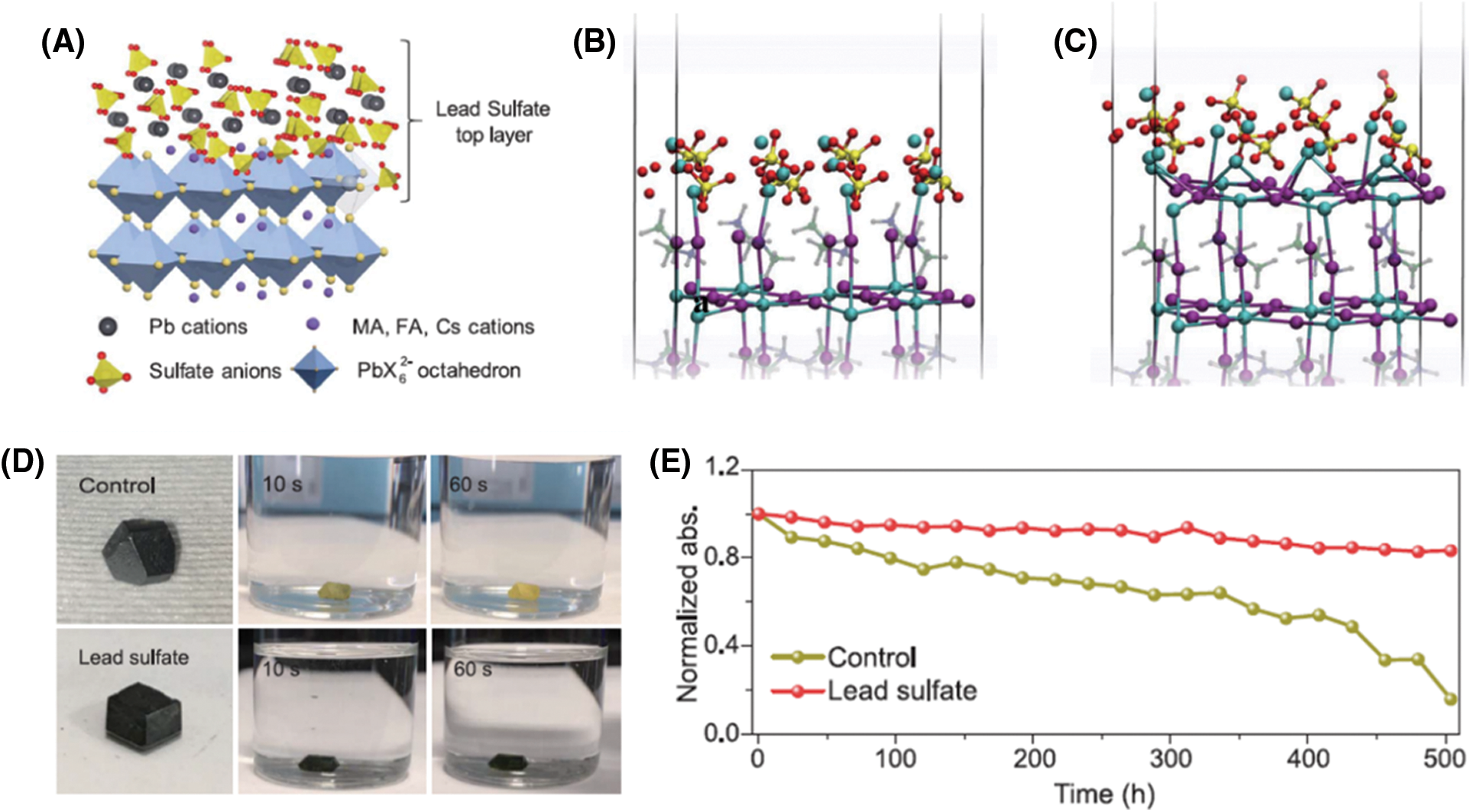
Figure 7: (A) Schematic diagram of the formation of lead sulfate layer on the surface of perovskite. (B–C) The optimized geometries of MAI-terminated (B) and PbI2-terminated (C) interface with a PbSO4 layer. (D) The changes with the time of MAPbI3 single crystal with and without lead sulfate top layer after being immersed in water. (E) Normalized absorbance decay at 740 nm for perovskite films sandwiched between PTAA and PCBM layers under simulated AM 1.5 G irradiation (100 mW cm−2) in ambient air. Adapted from Yang et al. [95] with permission from Science, Copyright 2019
Controlling the nucleation and growth of perovskite during the fabrication process is the key to obtaining uniform and high-quality perovskite absorber films. The development of process techniques, such as the antisolvent extraction and IEP methods, has enabled the preparation of high-quality perovskite films with low defect densities. In addition, a wide variety of additives are applied to tune the precursor colloid and to modulate the growth behaviour for achieving large grain sizes and high crystalline perovskite films. Furthermore, strategies are developed to passivate the defects, and various species of molecules have been employed and show great success in improving the PCE of PSCs.
However, the embedded perovskite-substrate interface passivation has received less success. Achieving effectively embedded perovskite interface passivation is important to further pursuing the theoretical limit of efficiency. Although many strategies have been developed in polycrystalline perovskite, their carrier transport and stability are still worse than that of single-crystal hybrid perovskites. Due to the absence of lattice applicable mismatched epitaxial substrates, the preparation of single-crystal PSCs remains a challenge. A strained epitaxial growth method and a solution-based lithography-assisted epitaxial-growth-and-transfer strategy are recently demonstrated and show great improvement in the single-crystal device, which encourages further investigation and development [98,99].
Funding Statement: The authors acknowledge funding support from the National Natural Science Foundation of China (52172182, 21975028).
Conflicts of Interest: The authors declare that they have no conflicts of interest to report regarding the present study.
References
1. Lee, M. M., Teuscher, J., Miyasaka, T., Murakami, T. N., Snaith, H. J. (2012). Efficient hybrid solar cells based on meso-superstructured organometal halide perovskites. Science, 338(6107), 643–647. [Google Scholar]
2. Yin, W. J., Shi, T., Yan, Y. (2014). Unique properties of halide perovskites as possible origins of the superior solar cell performance. Advanced Materials, 26(27), 4653–4658. [Google Scholar]
3. Xing, G., Mathews, N., Sun, S., Lim, S. S., Lam, Y. M. et al. (2013). Long-range balanced electron-and hole-transport lengths in organic-inorganic CH3NH3PbI3. Science, 342(6156), 344–347. [Google Scholar]
4. Stranks, S. D., Eperon, G. E., Grancini, G., Menelaou, C., Alcocer, M. J. et al. (2013). Electron-hole diffusion lengths exceeding 1 micrometer in an organometal trihalide perovskite absorber. Science, 342(6156), 341–344. [Google Scholar]
5. Kojima, A., Ikegami, M., Teshima, K., Miyasaka, T. (2012). Highly luminescent lead bromide perovskite nanoparticles synthesized with porous alumina media. Chemistry Letters, 41(4), 397–399. [Google Scholar]
6. Etgar, L., Gao, P., Xue, Z., Peng, Q., Chandiran, A. K. et al. (2012). Mesoscopic CH3NH3PbI3/TiO2 heterojunction solar cells. Journal of the American Chemical Society, 134(42), 17396–17399. [Google Scholar]
7. Dong, Q., Fang, Y., Shao, Y., Mulligan, P., Qiu, J. et al. (2015). Electron-hole diffusion lengths >175 μm in solution-grown CH3NH3PbI3 single crystals. Science, 347(6225), 967–970. [Google Scholar]
8. National Renewable Energy Laboratory. Best research-cellefficiency chart. https://www.nrel.gov/pv/cell-efficiency.html. [Google Scholar]
9. Ma, C., Park, N. G. (2020). A realistic methodology for 30% efficient perovskite solar cells. Chem, 6(6), 1254–1264. [Google Scholar]
10. Burschka, J., Pellet, N., Moon, S. J., Humphry-Baker, R., Gao, P. et al. (2013). Sequential deposition as a route to high-performance perovskite-sensitized solar cells. Nature, 499(7458), 316–319. [Google Scholar]
11. Jeon, N. J., Noh, J. H., Kim, Y. C., Yang, W. S., Ryu, S. et al. (2014). Solvent engineering for high-performance inorganic–organic hybrid perovskite solar cells. Nature Materials, 13(9), 897–903. [Google Scholar]
12. Jeon, N. J., Noh, J. H., Yang, W. S., Kim, Y. C., Ryu, S. et al. (2015). Compositional engineering of perovskite materials for high-performance solar cells. Nature, 517(7535), 476–480. [Google Scholar]
13. Yang, W. S., Noh, J. H., Jeon, N. J., Kim, Y. C., Ryu, S. et al. (2015). High-performance photovoltaic perovskite layers fabricated through intramolecular exchange. Science, 348(6240), 1234–1237. [Google Scholar]
14. Bi, D., Yi, C., Luo, J., Décoppet, J. D., Zhang, F. et al. (2016). Polymer-templated nucleation and crystal growth of perovskite films for solar cells with efficiency greater than 21%. Nature Energy, 1(10), 1–5. [Google Scholar]
15. Yang, W. S., Park, B. W., Jung, E. H., Jeon, N. J., Kim, Y. C. et al. (2017). Iodide management in formamidinium-lead-halide–based perovskite layers for efficient solar cells. Science, 356(6345), 1376–1379. [Google Scholar]
16. Jung, E. H., Jeon, N. J., Park, E. Y., Moon, C. S., Shin, T. J. et al. (2019). Efficient, stable and scalable perovskite solar cells using poly (3-hexylthiophene). Nature, 567(7749), 511–515. [Google Scholar]
17. Jiang, Q., Zhao, Y., Zhang, X., Yang, X., Chen, Y. et al. (2019). Surface passivation of perovskite film for efficient solar cells. Nature Photonics, 13(7), 460–466. [Google Scholar]
18. Yoo, J. J., Seo, G., Chua, M. R., Park, T. G., Lu, Y. et al. (2021). Efficient perovskite solar cells via improved carrier management. Nature, 590(7847), 587–593. [Google Scholar]
19. Jeong, J., Kim, M., Seo, J., Lu, H., Ahlawat, P. et al. (2021). Pseudo-halide anion engineering for α-FAPbI3 perovskite solar cells. Nature, 592(7854), 381–385. [Google Scholar]
20. Min, H., Lee, D. Y., Kim, J., Kim, G., Lee, K. S. et al. (2021). Perovskite solar cells with atomically coher ent interlayers on SnO2 electrodes. Nature, 598(7881), 444–450. [Google Scholar]
21. Luo, D., Su, R., Zhang, W., Gong, Q., Zhu, R. (2019). Minimizing non-radiative recombination losses in perovskite solar cells. Nature Reviews Materials, 5(1), 44–60. [Google Scholar]
22. Wei, X., Zhang, P., Bai, Y., Chen, Q. (2021). Electronic doping strategy in perovskite solar cells. Halide perovskites for photonics, pp. 3-1–3-56. USA: AIP Publishing Books. [Google Scholar]
23. Kim, J. Y., Lee, J. W., Jung, H. S., Shin, H., Park, N. G. (2020). High-efficiency perovskite solar cells. Chemical Reviews, 120(15), 7867–7918. [Google Scholar]
24. Lee, J. W., Lee, D. K., Jeong, D. N., Park, N. G. (2019). Control of crystal growth toward scalable fabrication of perovskite solar cells. Advanced Functional Materials, 29(47), 1807047. [Google Scholar]
25. Im, J. H., Kim, H. S., Park, N. G. (2014). Morphology-photovoltaic property correlation in perovskite solar cells: One-step versus two-step deposition of CH3NH3PbI3. APL Materials, 2(8), 081510. [Google Scholar]
26. Kojima, A., Teshima, K., Shirai, Y., Miyasaka, T. (2009). Organometal halide perovskites as visible-light sensitizers for photovoltaic cells. Journal of the American Chemical Society, 131(17), 6050–6051. [Google Scholar]
27. Eperon, G. E., Burlakov, V. M., Docampo, P., Goriely, A., Snaith, H. J. (2014). Morphological control for high performance, solution-processed planar heterojunction perovskite solar cells. Advanced Functional Materials, 24(1), 151–157. [Google Scholar]
28. Xiao, M., Huang, F., Huang, W., Dkhissi, Y., Zhu, Y. et al. (2014). A fast deposition-crystallization procedure for highly efficient lead iodide perovskite thin-film solar cells. Angewandte Chemie International Edition, 53(37), 9898–9903. [Google Scholar]
29. Ahn, N., Son, D. Y., Jang, I. H., Kang, S. M., Choi, M. et al. (2015). Highly reproducible perovskite solar cells with average efficiency of 18.3% and best efficiency of 19.7% fabricated via Lewis base adduct of lead (II) iodide. Journal of the American Chemical Society, 137(27), 8696–8699. [Google Scholar]
30. Yu, Y., Yang, S., Lei, L., Cao, Q., Shao, J. et al. (2017). Ultrasmooth perovskite film via mixed anti-solvent strategy with improved efficiency. ACS Applied Materials & Interfaces, 9(4), 3667–3676. [Google Scholar]
31. Yin, M., Xie, F., Chen, H., Yang, X., Ye, F. et al. (2016). Annealing-free perovskite films by instant crystallization for efficient solar cells. Journal of Materials Chemistry A, 4(22), 8548–8553. [Google Scholar]
32. Im, J. H., Jang, I. H., Pellet, N., Grätzel, M., Park, N. G. (2014). Growth of CH3NH3PbI3 cuboids with controlled size for high-efficiency perovskite solar cells. Nature Nanotechnology, 9(11), 927–932. [Google Scholar]
33. Pellet, N., Gao, P., Gregori, G., Yang, T. Y., Nazeeruddin, M. K. et al. (2014). Mixed-organic-cation perovskite photovoltaics for enhanced solar-light harvesting. Angewandte Chemie, 126(12), 3215–3221. [Google Scholar]
34. Ko, H. S., Lee, J. W., Park, N. G. (2015). 15.76% efficiency perovskite solar cells prepared under high relative humidity: Importance of PbI2 morphology in two-step deposition of CH3NH3PbI3. Journal of Materials Chemistry A, 3(16), 8808–8815. [Google Scholar]
35. Saliba, M., Matsui, T., Domanski, K., Seo, J. Y., Ummadisingu, A. et al. (2016). Incorporation of rubidium cations into perovskite solar cells improves photovoltaic performance. Science, 354(6309), 206–209. [Google Scholar]
36. Bi, D., Tress, W., Dar, M. I., Gao, P., Luo, J. et al. (2016). Efficient luminescent solar cells based on tailored mixed-cation perovskites. Science Advances, 2(1), e1501170. [Google Scholar]
37. Paek, S., Schouwink, P., Athanasopoulou, E. N., Cho, K., Grancini, G. et al. (2017). From nano-to micrometer scale: The role of antisolvent treatment on high performance perovskite solar cells. Chemistry of Materials, 29(8), 3490–3498. [Google Scholar]
38. Jeon, N. J., Na, H., Jung, E. H., Yang, T. Y., Lee, Y. G. et al. (2018). A fluorene-terminated hole-transporting material for highly efficient and stable perovskite solar cells. Nature Energy, 3(8), 682–689. [Google Scholar]
39. Min, H., Kim, M., Lee, S. U., Kim, H., Kim, G. et al. (2019). Efficient, stable solar cells by using inherent bandgap of α-phase formamidinium lead iodide. Science, 366(6466), 749–753. [Google Scholar]
40. Kim, G., Min, H., Lee, K. S., Lee, D. Y., Yoon, S. M. et al. (2020). Impact of strain relaxation on performance of α-formamidinium lead iodide perovskite solar cells. Science, 370(6512), 108–112. [Google Scholar]
41. Ummadisingu, A., Grätzel, M. (2018). Revealing the detailed path of sequential deposition for metal halide perovskite formation. Science Advances, 4(2), e1701402. DOI 10.1126/sciadv.1701402. [Google Scholar] [CrossRef]
42. Juarez-Perez, E. J., Ono, L. K., Qi, Y. (2019). Thermal degradation of formamidinium based lead halide perovskites into sym-triazine and hydrogen cyanide observed by coupled thermogravimetry-mass spectrometry analysis. Journal of Materials Chemistry A, 7(28), 16912–16919. DOI 10.1039/C9TA06058H. [Google Scholar] [CrossRef]
43. Kim, S. Y., Jo, H. J., Sung, S. J., Kim, D. H. (2016). Perspective: Understanding of ripening growth model for minimum residual PbI2 and its limitation in the planar perovskite solar cells. APL Materials, 4(10), 100901. DOI 10.1063/1.4963841. [Google Scholar] [CrossRef]
44. Cheng, Y., Li, H. W., Zhang, J., Yang, Q. D., Liu, T. et al. (2016). Spectroscopic study on the impact of methylammonium iodide loading time on the electronic properties in perovskite thin films. Journal of Materials Chemistry A, 4(2), 561–567. DOI 10.1039/C5TA08262E. [Google Scholar] [CrossRef]
45. Nie, W., Tsai, H., Asadpour, R., Blancon, J. C., Neukirch, A. J. et al. (2015). High-efficiency solution-processed perovskite solar cells with millimeter-scale grains. Science, 347(6221), 522–525. DOI 10.1126/science.aaa0472. [Google Scholar] [CrossRef]
46. Bai, S., Da, P., Li, C., Wang, Z., Yuan, Z. et al. (2019). Planar perovskite solar cells with long-term stability using ionic liquid additives. Nature, 571(7764), 245–250. DOI 10.1038/s41586-019-1357-2. [Google Scholar] [CrossRef]
47. Noel, N. K., Abate, A., Stranks, S. D., Parrott, E. S., Burlakov, V. M. et al. (2014). Enhanced photoluminescence and solar cell performance via Lewis base passivation of organic–inorganic lead halide perovskites. ACS Nano, 8(10), 9815–9821. DOI 10.1021/nn5036476. [Google Scholar] [CrossRef]
48. Han, J., Luo, S., Yin, X., Zhou, Y., Nan, H. et al. (2018). Hybrid PbS quantum-dot-in-perovskite for high-efficiency perovskite solar cell. Small, 14(31), 1801016. DOI 10.1002/smll.201801016. [Google Scholar] [CrossRef]
49. Li, X., Bi, D., Yi, C., Décoppet, J. D., Luo, J. et al. (2016). A vacuum flash–assisted solution process for high-efficiency large-area perovskite solar cells. Science, 353(6294), 58–62. DOI 10.1126/science.aaf8060. [Google Scholar] [CrossRef]
50. Yan, K., Long, M., Zhang, T., Wei, Z., Chen, H. et al. (2015). Hybrid halide perovskite solar cell precursors: Colloidal chemistry and coordination engineering behind device processing for high efficiency. Journal of the American Chemical Society, 137(13), 4460–4468. DOI 10.1021/jacs.5b00321. [Google Scholar] [CrossRef]
51. McMeekin, D. P., Wang, Z., Rehman, W., Pulvirenti, F., Patel, J. B. et al. (2017). Crystallization kinetics and morphology control of formamidinium–cesium mixed-cation lead mixed-halide perovskite via tunability of the colloidal precursor solution. Advanced Materials, 29, 1607039. [Google Scholar]
52. Noel, N. K., Congiu, M., Ramadan, A. J., Fearn, S., McMeekin, D. P. et al. (2017). Unveiling the influence of pH on the crystallization of hybrid perovskites, delivering low voltage loss photovoltaics. Joule, 1(2), 328–343. [Google Scholar]
53. McMeekin, D. P., Sadoughi, G., Rehman, W., Eperon, G. E., Saliba, M. et al. (2016). A mixed-cation lead mixed-halide perovskite absorber for tandem solar cells. Science, 351(6269), 151–155. [Google Scholar]
54. Jin, B., Ming, Y., Wu, Z., Cao, J., Liu, Y. et al. (2022). Silk fibroin induced homeotropic alignment of perovskite crystals toward high efficiency and stability. Nano Energy, 94, 106936. [Google Scholar]
55. Zhao, J. H., Mu, X., Wang, L., Fang, Z., Zou, X. et al. (2022). Homogeneously large polarons in aromatic passivators improves charge transport between perovskite grains for >24% efficiency in photovoltaics. Angewandte Chemie International Edition, 61(14), e202116308. DOI 10.1002/anie.202116308. [Google Scholar] [CrossRef]
56. Jiang, L. L., Wang, Z. K., Li, M., Zhang, C. C., Ye, Q. Q. et al. (2018). Passivated perovskite crystallization via g-C3N4 for high-performance solar cells. Advanced Functional Materials, 28(7), 1705875. [Google Scholar]
57. Deng, Y., Zheng, X., Bai, Y., Wang, Q., Zhao, J. et al. (2018). Surfactant-controlled ink drying enables high-speed deposition of perovskite films for efficient photovoltaic modules. Nature Energy, 3(7), 560–566. [Google Scholar]
58. Zhou, H., Chen, Q., Li, G., Luo, S., Song, T. B. et al. (2014). Interface engineering of highly efficient perovskite solar cells. Science, 345(6196), 542–546. [Google Scholar]
59. Williams, S. T., Zuo, F., Chueh, C. C., Liao, C. Y., Liang, P. W. et al. (2014). Role of chloride in the morphological evolution of organo-lead halide perovskite thin films. ACS Nano, 8(10), 10640–10654. [Google Scholar]
60. Tidhar, Y., Edri, E., Weissman, H., Zohar, D., Hodes, G. et al. (2014). Crystallization of methyl ammonium lead halide perovskites: Implications for photovoltaic applications. Journal of the American Chemical Society, 136(38), 13249–13256. [Google Scholar]
61. Zhao, Y., Zhu, K. (2014). CH3NH3Cl-assisted one-step solution growth of CH3NH3PbI3: Structure, charge-carrier dynamics, and photovoltaic properties of perovskite solar cells. The Journal of Physical Chemistry C, 118(18), 9412–9418. [Google Scholar]
62. Yu, H., Wang, F., Xie, F., Li, W., Chen, J. et al. (2014). The role of chlorine in the formation process of “CH3NH3PbI3-xClx” perovskite. Advanced Functional Materials, 24(45), 7102–7108. [Google Scholar]
63. Guan, J., Liu, N. (2016). Exploitative and exploratory innovations in knowledge network and collaboration network: A patent analysis in the technological field of nano-energy. Research Policy, 45(1), 97–112. [Google Scholar]
64. Xie, F. X., Zhang, D., Su, H., Ren, X., Wong, K. S. et al. (2015). Vacuum-assisted thermal annealing of CH3NH3PbI3 for highly stable and efficient perovskite solar cells. ACS Nano, 9(1), 639–646. [Google Scholar]
65. Kim, M., Kim, G. H., Lee, T. K., Choi, I. W., Choi, H. W. et al. (2019). Methylammonium chloride induces intermediate phase stabilization for efficient perovskite solar cells. Joule, 3(9), 2179–2192. [Google Scholar]
66. Wang, Z., Liu, L., Liu, X., Song, D., Shi, D. et al. (2022). Uncovering synergistic effect of chloride additives for efficient quasi-2D perovskite solar cells. Chemical Engineering Journal, 432, 134367. [Google Scholar]
67. Zuo, C., Ding, L. (2014). An 80.11% FF record achieved for perovskite solar cells by using the NH4Cl additive. Nanoscale, 6(17), 9935–9938. [Google Scholar]
68. Liu, H., Dong, M., Huang, W., Gao, J., Dai, K. et al. (2017). Lightweight conductive graphene/thermoplastic polyurethane foams with ultrahigh compressibility for piezoresistive sensing. Journal of Materials Chemistry C, 5(1), 73–83. [Google Scholar]
69. Zhao, P., Kim, B. J., Jung, H. S. (2018). Passivation in perovskite solar cells: A review. Materials Today Energy, 7, 267–286. [Google Scholar]
70. Wang, J. T. W., Wang, Z., Pathak, S., Zhang, W., deQuilettes, D. W. et al. (2016). Efficient perovskite solar cells by metal ion doping. Energy & Environmental Science, (9), 2892–2901. [Google Scholar]
71. Abdi-Jalebi, M., Dar, M. I., Sadhanala, A., Senanayak, S. P., Franckevičius, M. et al. (2016). Impact of monovalent cation halide additives on the structural and optoelectronic properties of CH3NH3PbI3 perovskite. Advanced Energy Materials, 6(10), 1502472. DOI 10.1002/aenm.201502472. [Google Scholar] [CrossRef]
72. Son, D. Y., Kim, S. G., Seo, J. Y., Lee, S. H., Shin, H. et al. (2018). Universal approach toward hysteresis-free perovskite solar cell via defect engineering. Journal of the American Chemical Society, 140(4), 1358–1364. DOI 10.1021/jacs.7b10430. [Google Scholar] [CrossRef]
73. Chatterjee, S., Pal, A. J. (2018). Influence of metal substitution on hybrid halide perovskites: Towards lead-free perovskite solar cells. Journal of Materials Chemistry A, 6(9), 3793–3823. DOI 10.1039/C7TA09943F. [Google Scholar] [CrossRef]
74. Wang, H., Liu, H., Dong, Z., Wei, X., Song, Y. et al. (2022). Extracting ammonium halides by solvent from the hybrid perovskites with various dimensions to promote the crystallization of CsPbI3 perovskite. Nano Energy, 94, 106925. DOI 10.1016/j.nanoen.2022.106925. [Google Scholar] [CrossRef]
75. Tan, S., Shi, J., Yu, B., Zhao, W., Li, Y. et al. (2021). Inorganic ammonium halide additive strategy for highly efficient and stable CsPbI3 perovskite solar cells. Advanced Functional Materials, 31(21), 2010813. DOI 10.1002/adfm.202010813. [Google Scholar] [CrossRef]
76. Li, Y., Chen, Z., Yu, B., Tan, S., Cui, Y. et al. (2022). Efficient, stable formamidinium-cesium perovskite solar cells and minimodules enabled by crystallization regulation. Joule, 6(3), 676–689. DOI 10.1016/j.joule.2022.02.003. [Google Scholar] [CrossRef]
77. Cho, S. P., Shin, J. C., Lee, H. J., Lee, M., Na, S. I. et al. (2022). Multi-functional cyclic ammonium chloride additive for efficient and stable air-processed perovskite solar cells. Journal of Power Sources, 531, 231243. DOI 10.1016/j.jpowsour.2022.231243. [Google Scholar] [CrossRef]
78. Aydin, E., De Bastiani, M., De Wolf, S. (2019). Defect and contact passivation for perovskite solar cells. Advanced Materials, 31(25), 1900428. DOI 10.1002/adma.201900428. [Google Scholar] [CrossRef]
79. Li, Y., Wu, H., Qi, W., Zhou, X., Li, J. et al. (2020). Passivation of defects in perovskite solar cell: From a chemistry point of view. Nano Energy, 77, 105237. DOI 10.1016/j.nanoen.2020.105237. [Google Scholar] [CrossRef]
80. Gao, F., Zhao, Y., Zhang, X., You, J. (2020). Recent progresses on defect passivation toward efficient perovskite solar cells. Advanced Energy Materials, 10(13), 1902650. DOI 10.1002/aenm.201902650. [Google Scholar] [CrossRef]
81. Chen, J., Seo, J. Y., Park, N. G. (2018). Simultaneous improvement of photovoltaic performance and stability by in situ formation of 2D perovskite at (FAPbI3)0.88 (cspbbr3)0.12/CuSCN interface. Advanced Energy Materials, 8(12), 1702714. DOI 10.1002/aenm.201702714. [Google Scholar] [CrossRef]
82. Wei, X., Xiao, M., Wang, B., Wang, C., Li, Y. et al. (2022). Avoiding structural collapse to reduce lead leakage in perovskite photovoltaics. Angewandte Chemie, e202204314. DOI 10.1002/ange.202204314. [Google Scholar] [CrossRef]
83. Shao, Y., Xiao, Z., Bi, C., Yuan, Y., Huang, J. (2014). Origin and elimination of photocurrent hysteresis by fullerene passivation in CH3NH3PbI3 planar heterojunction solar cells. Nature Communications, 5(1), 1–7. DOI 10.1038/ncomms6784. [Google Scholar] [CrossRef]
84. de Bastiani, M., Dell’Erba, G., Gandini, M., D’Innocenzo, V., Neutzner, S. et al. (2016). Solar cells: Ion migration and the role of preconditioning cycles in the stabilization of the J–V characteristics of inverted hybrid perovskite solar cells (Adv. Energy Mater. 2/2016). Advanced Energy Materials, 6(2). DOI 10.1002/aenm.201670009. [Google Scholar] [CrossRef]
85. Xu, J., Buin, A., Ip, A. H., Li, W., Voznyy, O. et al. (2015). Perovskite–fullerene hybrid materials suppress hysteresis in planar diodes. Nature Communications, 6(1), 7081. DOI 10.1038/ncomms8081. [Google Scholar] [CrossRef]
86. Wang, Q., Dong, Q., Li, T., Gruverman, A., Huang, J. (2016). Thin insulating tunneling contacts for efficient and water-resistant perovskite solar cells. Advanced Materials, 28(31), 6734–6739. DOI 10.1002/adma.201600969. [Google Scholar] [CrossRef]
87. Deng, H., Yang, X., Dong, D., Li, B., Yang, D. et al. (2015). Flexible and semitransparent organolead triiodide perovskite network photodetector arrays with high stability. Nano Letters, 15(12), 7963–7969. DOI 10.1021/acs.nanolett.5b03061. [Google Scholar] [CrossRef]
88. Li, J., Si, J., Gan, L., Liu, Y., Ye, Z. et al. (2016). Simple approach to improving the amplified spontaneous emission properties of perovskite films. ACS Applied Materials & Interfaces, 8(48), 32978–32983. DOI 10.1021/acsami.6b13289. [Google Scholar] [CrossRef]
89. Kumar, S., Dhar, A. (2016). Accelerated thermal-aging-induced degradation of organometal triiodide perovskite on ZnO nanostructures and its effect on hybrid photovoltaic devices. ACS Applied Materials & Interfaces, 8(28), 18309–18320. DOI 10.1021/acsami.6b06878. [Google Scholar] [CrossRef]
90. Zuo, L., Guo, H., deQuilettes, D. W., Jariwala, S., de Marco, N. et al. (2017). Polymer-modified halide perovskite films for efficient and stable planar heterojunction solar cells. Science Advances, 3(8), e1700106. DOI 10.1126/sciadv.1700106. [Google Scholar] [CrossRef]
91. Huang, X., Guo, H., Wang, K., Liu, X. (2017). Ionic liquid induced surface trap-state passivation forefficient perovskite hybrid solar cells. Organic Electronics, 41, 42–48. [Google Scholar]
92. Zhu, X., Yang, S., Cao, Y., Duan, L., Du, M. et al. (2022). Ionic-liquid-perovskite capping layer for stable 24.33%-efficient solar cell. Advanced Energy Materials, 12(6), 2103491. [Google Scholar]
93. Peng, M., Dai, W., Lin, L., Xiao, B., Guo, S. et al. (2021). Performance improvement of perovskite solar cells by using ionic liquid BMIMPF6 as an interface modifier. ACS Applied Energy Materials, 4(11), 12421–12428. [Google Scholar]
94. Qi, W., Zhou, X., Li, J., Cheng, J., Li, Y. et al. (2020). Inorganic material passivation of defects toward efficient perovskite solar cells. Science Bulletin, 65(23), 2022–2032. [Google Scholar]
95. Yang, S., Chen, S., Mosconi, E., Fang, Y., Xiao, X. et al. (2019). Stabilizing halide perovskite surfaces for solar cell operation with wide-bandgap lead oxysalts. Science, 365(6452), 473–478. [Google Scholar]
96. Xie, L., Zhang, T., Zhao, Y. (2020). Stabilizing the MAPbI3 perovksite via the in-situ formed lead sulfide layer for efficient and robust solar cells. Journal of Energy Chemistry, 47, 62–65. [Google Scholar]
97. Li, X., Zhang, W., Guo, X., Lu, C., Wei, J. et al. (2022). Constructing heterojunctions by surface sulfidation for efficient inverted perovskite solar cells. Science, 375(6579), 434–437. [Google Scholar]
98. Chen, Y., Lei, Y., Li, Y., Yu, Y., Cai, J. et al. (2020). Strain engineering and epitaxial stabilization of halide perovskites. Nature, 577(7789), 209–215. [Google Scholar]
99. Lei, Y., Chen, Y., Zhang, R., Li, Y., Yan, Q. et al. (2020). A fabrication process for flexible single-crystal perovskite devices. Nature, 583(7818), 790–795. [Google Scholar]
 | This work is licensed under a Creative Commons Attribution 4.0 International License, which permits unrestricted use, distribution, and reproduction in any medium, provided the original work is properly cited. |