Materials
| Journal of Renewable Materials |
DOI: 10.32604/jrm.2021.015465
ARTICLE
Physical Properties of SiC Nanostructure for Optoelectronics Applications
1Applied Science Department, University of Technology-Iraq, Baghdad, 10066, Iraq
2Laser and Optoelectronic Engineering Department, University of Technology-Iraq, Baghdad, 10066, Iraq
*Corresponding Authors: Evan T. Salim. Email: evan.t.salim@uotechnology.edu.iq; Makram A. Fakhri. Email: makram.a.fakhri@uotechnology.edu.iq
Received: 20 December 2020; Accepted: 18 January 2021
Abstract: A SiC nanofilms have been deposited and investigated on quartz and silicon substrates using pulsed laser deposition technique with the 300 pulses of Nd: YAG laser at two different laser wavelengths of 1064 nm and 532 nm. The structural, morphological, and optical properties of the deposited nanostructure SiC were prepared and characterized as a function of the wavelengths of the used laser. The structural result shows four different pecks at (111), (200), (220), and (311) planes related to Nano SiC. The transmission result presents that the optical energy gap value for the SiC nanostructure is depended on the wavelength of the used laser and it is found about the range (3.03 eV–3.23 eV). The investigations of the SEM and AFM show that the prepared SiC Nano-films having a grain size range (36.34–48.75) nm and roughness about 4.462 to 3.062 nm. SiC/Si hetero-junction devices show an enhanced performance at 532 nm.
Keywords: Pulsed Laser deposition; nanostructure; 4H-SiC; PLD; heterostructure; nanofilms
Silicon carbide (SiC) are amongst the materials with the widest optical energy gap abut (2.0 eV ≤ E ≤ 7.0 eV) [1−4]. This behavior allows the production of UV detectors to be used [5,6]. The SiC-integrated photodetectors are capable of producing high signal-to-noise ratios that work for solar-blinds [7−9].
SiC Nanostructures are attracted due to their perfect properties such as the high values of the thermal, the wide-optical bandgap semiconducting materials, the stability of the chemical, large mobility, high breakdown of the field strength, and high-temperature resistance [10−12].
The structural, the morphological, and the optical properties (the physical properties) of the nanostructures of the SiC are greatly influenced by the carbon and the silicon film contents, and therefore, the preparation methods, as well as Si and C sources, are of interest [13−15].
In recent years, it got good competition for various traditional materials for different multi-disciplinary implementation. It is premium properties such as (the electronic and the electrical) make it favorable materials are using for the next-generation optoelectronic, and photonic devices [16–18]. Recently, Kaur et al. [19] deposited the Nanostructure of β-SiC, which was conducted selective growth for β-SiC by laser irradiation excimer of the PMMA (polymethyl methacrylate) [20,21].
It has been widely used in different applications such the Nanoelectronics, optoelectronics, the LED (light-emitting diodes), and the photonic [22], cells of the photoelectrochemical [23], photocatalyst [24], different sensor [25], and the energy storage [26].
Several different synthesis methods, techniques, and gases were used in the preparation and deposition of the SiC or its nanostructures with the electrical, electronic, and other required physical properties at the relatively low values of the substrate temperatures such as CVD (chemical vapor deposition) [27−29], MBE (molecular beam epitaxy) [30,31]. Sol-gel and electrospinning [32−34], Pulsed laser ablation in liquids [35] PE-CVD (chemical vapor deposition enhanced by plasma) [36], PLD (pulsed laser deposition) [37], and the MBE (molecular beam epitaxy) [38].
The (PLD) Laser pulse deposition, is used the method on a large scale and allows the growth of super-conductors with high temperatures. This technique is run at a low temperature relatively and is capable of producing Nano thin films (silicon carbide is amorphous or polycrystalline) [39−42]. This method has several advantages, such as the activation of the types extracted from the user and the selected target. This will enhance the chemical nature of film surface growth, which reduces the requirements for the activation of the surfaces [43−48]. Moreover, there is a control for the thickness of the deposited films by controlling the growth of the kinetics, simply by manipulating the (frequency) or the repetition rate and the used laser power in addition to the deposition pressure [49−53].
In this work, a two laser wavelengths has been used to prepare SiC nanostructure on the quartz and Si substrates. The physical properties of thin films and SiC/Si device performance have been investigated.
A high purity powder (99.99%) of the SiC from Aldrich was used in the (Pulsed Laser Deposition) PLD method and was prepared by pressing the powder of the SiC using a hydraulic press (15 Tonne) to get a pellet property diameter of 25 mm and a height of 5 mm. A Q-Switching- Nd: YAG laser RY 280, Chin, of 300 pulses of laser, 6 ns of the pulse duration, With an average frequency of three Hz/sec., and 1500 mJ energy of the used laser to deposit the material of the prepared targets on a substrate of the quartz at the different laser wavelength. PLD mechanism include the ablation of the target material employing short pulses of laser wavelength as energy source, such that the ablated particle deposited on the desired substrate in a vacuum environment. The powder material is compressed under high mechanical pressure to take a pellet shape.
The different laser wavelength of (1064 nm and 532 nm) was used to ablate the substrate during the deposition process under vacuum pressure of about 10-3 mbar. After finishing the process of deposition, the deposited Nanofilms were undergoing a process of annealing at 400°C for 4 h. A Double-beam from (Shimadzu UV-Vis 1800, Japan) spectrophotometer has tested the transmissions and the absorptions of the deposited films at the range of the wavelength (300–800) nm, and also the value of the energy bandgap (Eg) was calculated depending on the (transmission) T%, and the (absorption ) A%, the relation between A, T, and reflection are A + T + R = 1 since the optical beam has a vertical incidence on the sample there for the R assume to be zero, and the results related to the absorption and hence the transmission from the film.
X-ray diffraction system (X’Pert Pro MRD PW3040) with the Cu-Kα radiation where λ = 0.15418 nm was used to tests the properties of the structure for the SiC Nanofilms.
Scanning Probe Microscope of (SPM-9600), from the Japan (Shimadzu company), and the (JOEL JSM-6460LV, Oxford Instruments Analytical, Ltd., Tarvonsalmenkatu, Finland) device from Japan has been used to exam the final properties of the topography for the Nanofilms deposited, that are represented by the AFM, and SEM, respectively.
A single crystalline silicon substrate of 1–6 Ω cm electrical resistivity’s was used for device manufacturing; a figure print like aluminum mask has been deposited to maintained the device performance. To investigate I-V in dark and illumination using (DF LT30/2) Power Supply, (UNI-T-UT33C) and (TEKR. CDM 250) Digital Multi-meters. The C-V results were tested using RCL programmable Meter from (Fluke PM6306). Finally, the value of the spectral responsivity of the silicon carbide heterostructure was tested at the region of the spectral of (200 nm–900 nm) using an optical monochromator. All the previous tests were carried out in the temperature room.
Fig. 1 shows the transmission spectrums of the SiC Nano thin films, the deposition conditions seem to have a strong and direct effect on the optical properties of the films. In general, the value of transmission displayed a relative increase in their value from 81.9% to 96.2%, with the changes in laser wavelength from 1064 nm to 532 nm, respectively. The low value of the transmission in the region of UV, as a part of the physical properties of the silicon carbide, where its values are related to the value of the optical bandgap in the Uv-region. At the visible region, the optical transmission as a high value indicates the low values of the surface roughness and very good homogeneous films [12,54,55].
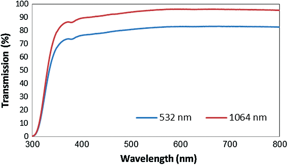
Figure 1: Optical transmission spectrum of Nano SiC deposited at various laser wavelengths
The absorption spectrums of the SiC Nano-films at different laser wavelengths have been presented in Fig. 2. The absorption (A) values were estimated based on the values of the transmission. It is observed that the values of the optical absorption were decreased by using the Second Harmonic Generation (SHG) Nd-YAG laser; this will be suitable for using such film in optoelectronic device fabrication where window effect will be dependent for the hetero-junction device. Then elevated absorption value near 300 nm is related to cut off wavelength of the SiC bandgap after which the material is transparent to all incident wavelengths.
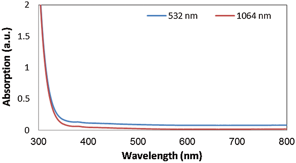
Figure 2: Spectrum of the absorption of Nano SiC deposited at different laser wavelengths
The value of the energy bandgap (Eg) for the deposited SiC was evaluated by extrapolated the straight line of the curve between the photon energy (hν) and (αhν)². The intersection of this drawn straight line with the main curve on the x-axis corresponds to the value of the optical energy bandgap as presents in Fig. 3. The bandgap values of the deposited Nano SiC films are around 303 eV and 3.23 eV for both 1064 nm and 532 nm, respectively. The reduction in bandgap value at the SHG wavelength may be related to increases in the laser flounce which resulted in decreases in the particles size, therefore according to the Burstein Moss–effect, the energy gap-related inversely to the particle size, and also because the increase in the sizes of the grains leads to a high crystallization which means less stress in the film. That could result in an increase in the bandgap as a result of the reduction of the crystal defects inside the material [56,57].
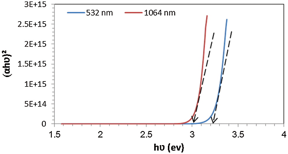
Figure 3: Optical energy band gap spectrum of Nano SiC deposited at various laser wavelengths
Fig. 4 present the patterns of the x-ray diffractions (XRD) for the Nano SiC films deposited at different wavelengths of Laser. The SiC Nanofilms X-ray pattern is deposited at 1064 nm exhibits four peaks manifest at the angles of diffraction of 35.42° and 42.54°, 60.82° and 73.24° corresponds to the planes of (111), (200), (220), and (311), respectively. When decreased the wavelength of the used laser to 532 nm, the pattern of the x-ray (XRD) of the deposited SiC shows the presence of the same peaks fastened at angles of the diffraction of 35.42° and 42.54°, 60.82° and 73.24° corresponds to the planes of (111), (200), (220), and (311) respectively but it differs in the intensities. All the present peaks in both wavelengths used in the preparation are indexed to the structure type of hexagonal and it appears to 4H-SiC depending on the card (JCPDS #22-1317). Moreover, it clearly presents that the values of the intensity for the pattern of the XRD peaks were enhanced and increased with the increase in the wavelength of the used laser as a result of an increase in grain size and as a result of promotion of the quality of the crystals (high crystenality) [25,58].
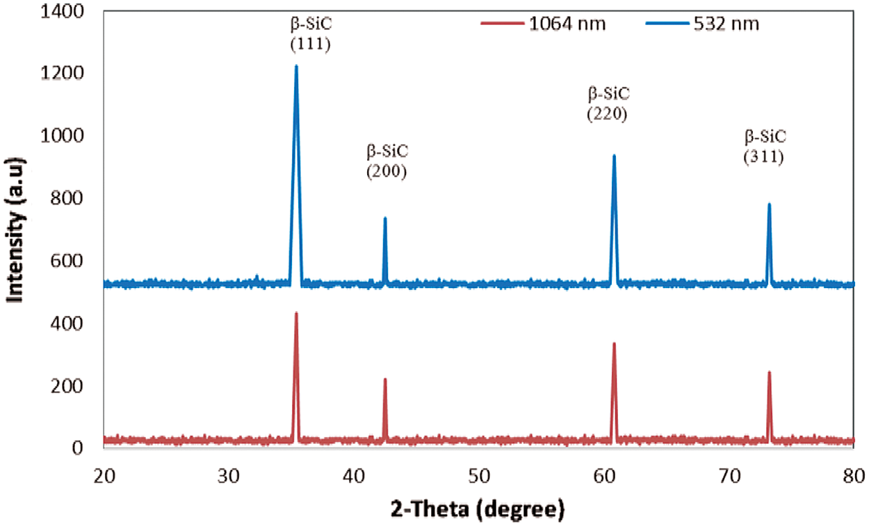
Figure 4: XRD patterns of SiC Nanofilm on quartz substrate at various laser wavelengths
The estimated values of the average size of the grains, the roughness, and the root mean square RMS values for the Nanofilms of the deposited SiC on the quartz substrates at different laser wavelengths based on the atomic force microscopy (AFM) results are presented in Fig. 5. The results show the regular density surface with a uniform distribution of the deposited grains throughout the surface. The presented results are indicating that the average diameter of the grains is inversely proportional to the used Laser wavelength. Where these values changed from (36.34–48.75) nm where the grains of 86 nm for the used laser wavelength are 532 nm and the grains of 98 nm for the used laser wavelength are 1065 nm. Thus, it can be shown that the increase in the used laser wavelength means an identical increase in the values of the optical bandgap of the prepared and deposited Nanofilms. In conjunction with the decreasing of the used laser wavelength, the values of the mean roughness and the RMS roughness are decreased. Where, the values of the average roughness are increased from (2.1 to 3.3) nm, while the RMS roughness increased from (3.062 to 4.462) nm. Controlling the RMS roughness and the average roughness is very important in optoelectronics devices using SiC Nanofilm. All estimated constants of the surface are tabulated below in Tab. 1.
Table 1: The average of the roughness, diameters, and root mean square values of Nano film SiC nanostructure thin film deposited at various laser wavelengths
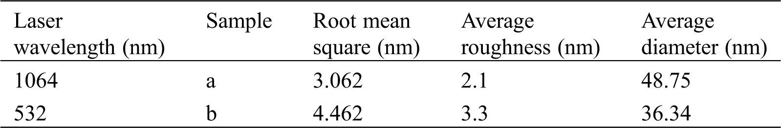
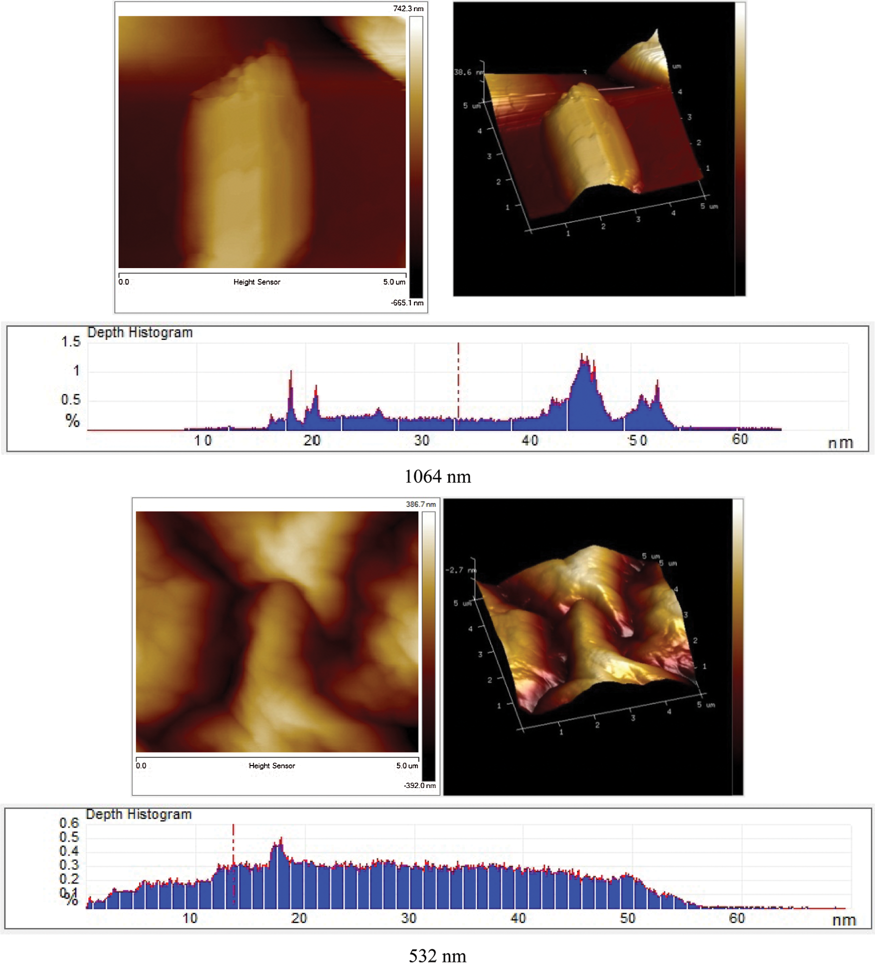
Figure 5: Images of the AFM for Nano SiC films deposited at various laser wavelengths
Fig. 6a presents the images of the results of SEM for the Nanofilms of the SiC production at different laser wavelengths using the PLD method. The size and the morphology of the deposited SiC Nanofilms are clearly dependent strongly on the wavelength of the used laser. It is clear that of the presented images there is a mixture of Nano-sized spherical particles and Nano flakes that are horizontally grown. For the deposited Nanofilms of the SiC synthesized with 532 nm wavelength of the used laser it clear that the number of Nano spherical grains is more distributed from the flakes, and the average of these particle sizes was about 65 nm and the average size of the flakes were about 85 nm. The concentration of SiC nanofilms increased as the used laser wavelength is decreased to 532 nm. The images of the SEM are confirmed that the number of lumpy grains (Nano flakes) was increased at the high laser wavelength because of the laser wavelength increase due to the reduction of the incident beam energy which results in lowering the particle size. The EDX result shows in Fig. 6b insure the successful formation of the SiC nanostructure.
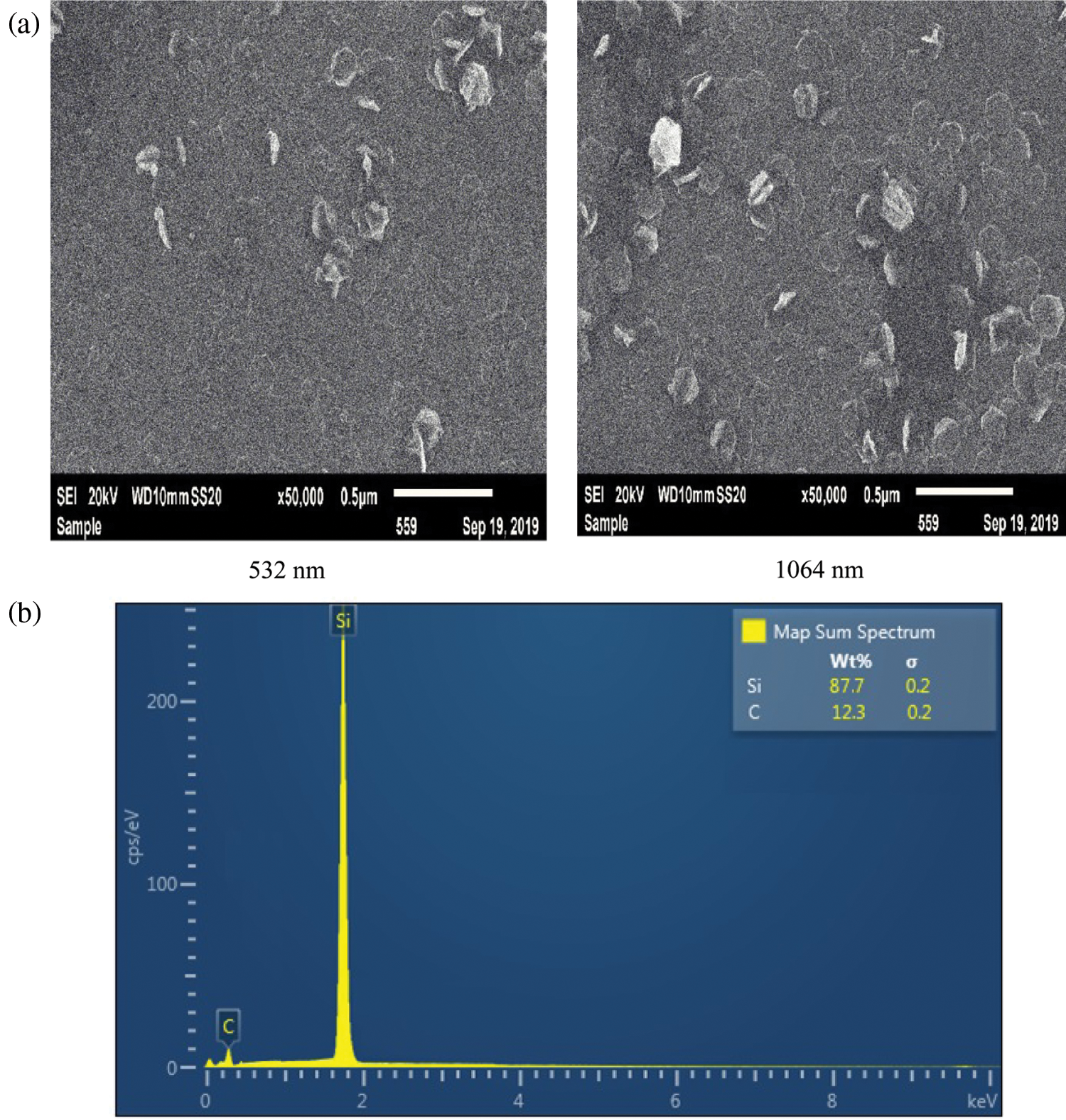
Figure 6: (a) Images of the SEM for Nano SiC films deposited at various laser wavelengths. (b) EDX result of Nano SiC films deposited at 532 nm
Fig. 7 presents the dark electrical (I-V) properties at the temperature of the room over a range of applied voltage (−3–+3 volts) of nano silicon carbide deposited/Si heterostructure deposited at the different pulsed laser wavelength. All the variants of the heterojunctions present good characteristics of ratification comparing with the wafer of the Silicone which indicates the fabrication of a device diode-like. The value of the current at the forward bias has been doubled very dramatically with a value of the biasing voltage, where the tested currents are very small at the value of the biasing voltage are small, these current named a recombination current, while at the higher biasing voltage >1 V, the value of the diffusion current was controlled. From the figure below it is clear that the synthesized heterojunction using the second harmonic generation gives a larger value of a forward current as a result of reducing the resistivity of the layer of the silicon carbide.
Figure 7: I-V characteristic at the Dark of silicone carbide heterostructure and Si wafer
Fig. 7 also shows the I-V properties of the silicon wafer that did not exhibit any correction properties (roughly seen as an ohmic contact). Fig. 8 presents the electrical (I-V) characteristics under the illumination of halogen light of the intensity of 65 mW/cm2 for the deposited nano SiC/Si photodetectors deposited at the various pulsed laser wavelength. It is clear that the value of the reverse current has been increased after illumination as a result of the pairs of the electrons- holes generation at the region of the depletion and the length of the carrier diffusion. It is clear that the reduction in pulsed laser wavelength (using second harmonic generation) leads to increasing the illumination current. Where no saturation is observed in the value of the photo-current when illuminated, and this indicates the quality of the linear characteristics used for fabricating an optoelectronic device such as the photodetectors. The presented figure also shows the heterogeneity of the fabricated heterojunction at the wavelength variation of the pulsed laser used in the deposition, which is due to the increase in the amount of light absorption and as a result of the increased concentration of the silicon carbide nanoparticles, as well as the expansion of the depletion region width and the increase in the carrier spread length. Moreover, there are some factors affecting the optical current values of the photodetectors such as grain size and surface morphology as well as the surface chemistry of SiC nanoparticles also affect.
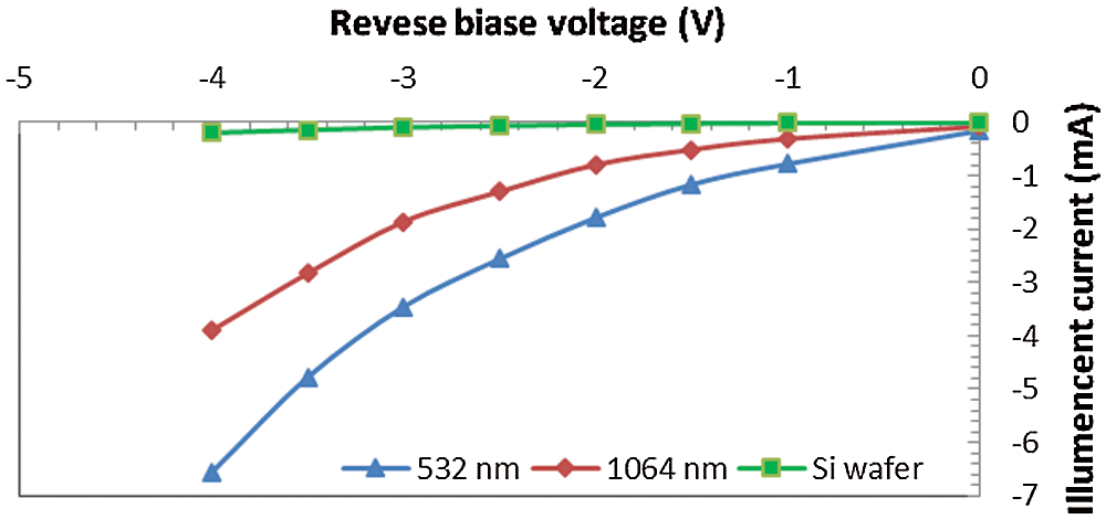
Figure 8: I-V result at Illuminated of nano silicon carbide heterostructure
Fig. 9 presented the relationship of the squared reciprocal of the tested capacitance (C−2) with the voltage at the reverse bias for the deposited nano SiC heterostructure, where the presented linear relationship shows that the type of the deposited junction is an abrupt junction. The value of the potential Built-in has been determined by extrapolating the linear portion of the presented curve to the value of the 1/C2 equal to 0 points. The estimated Vbi values have been found lower than the estimated values of the voltage turn-on from I-V properties as a result of the high resistivity of silicon carbide nanostructures. The values of the Built-in potential were reduced with the decrease in the laser wavelength (using second harmonic generation)can be related to the difference of each concentration of the electrons for the nano silicon carbide structure and the width of the depletion region with the wavelength of the pulsed laser.
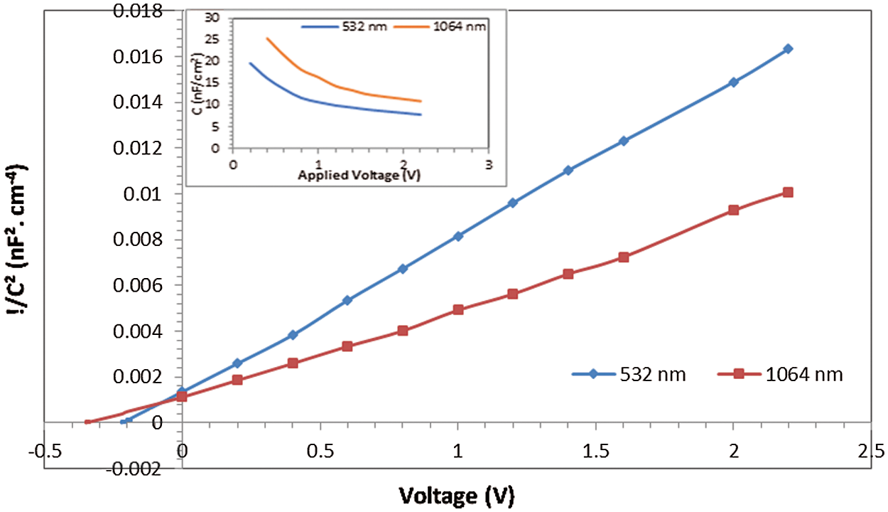
Figure 9: C-V and 1/C2 as a fuction of voltage of SiC heterostructure
Fig. 10 presents the spectral responsivity for the silicon carbide nano heterostructure at the bias of 5 volts, it has clearly seen that two featured regions of the response, the first one peaked at ~375 nm as the edge of the absorption of the nano silicon carbide heterostructure, and the second one is peaked at ~715 nm as the edge of the absorption of the substrate of the nano silicon wafer. The value of the optical responsivity of the photodetector at 375 nm has been increased from 1.3 AW−1 to 1.62 AW−1 as the wavelength of the pulsed laser decreased (using second harmonic generation) from 1064 nm to 532 nm, these increasing as a result of an increase in the width of the depletion region and the length of the diffusion, increasing the efficiency of the carrier collection, increasing the absorption of the photons at the region of the depletion.
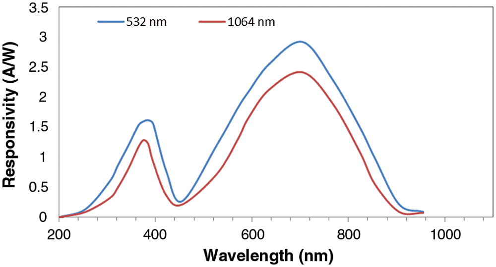
Figure 10: Responsivity of nano silicon carbide heterostructure
Fig. 11 presents the effect of the pulsed laser wavelength on the specific detectivity D* of the heterostructure for the nano silicon carbide. The values of the detectivity are dependent on the current noise and the values of the spectral responsivity which is presented previously as a function of the pulsed laser wavelength. while the decrease in the values of the leakage current causes an increase in the values of the detectivity of the fabricated photodetector, the values of the specific detectivity change with a value of the wavelengths exactly the same presented in the values of the spectral responsivity. Also, it has been found two presented peaks along the applied wavelength with the different pulsed laser wavelength. The high-value detectivity (177 × 1012 W−1 cm Hz0.5 at the wavelength of 376 nm and 321 × 1012 W−1 cm Hz0.5 at the wavelength of 715 nm) whereas, the fabricated photodetectors and their results presented here can be used to and sense detects the UV signals and the weak Near Infra-Read signals.
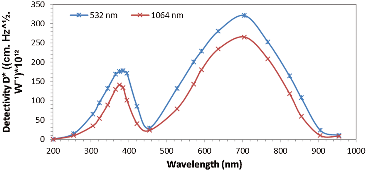
Figure 11: Laser wavelength effects on specific detectivity for silicon carbide heterostructure
High performance SiC/Si heterojunction device could be successfully prepared using simple, low temperature, PLD technique at second harmonic ND-Yag laser. A mixture of Nano-sized spherical particles about 36 nm size and Nano flake that are horizontally grown about 48 nm sizes with hexagonal single-crystal could be obtained. The bandgap values of the deposited Nano SiC films are increases as laser wavelength increase and its values around from 2.94 eV to 3.14 eV, the shifts towered the blue region were shown for SiC nanofilms prepared at low laser wavelength. The device performance results confirmed the presence of two response peaks at 375 nm and 715 nm, respectively. The high response of the fabricated devices (photodetectors) in the region of the Ultra-Violet indicates that the technology used here is encouraging and promising for fabricating cost-effective and simple Ultra-Violet detectors.
Funding Statement: The authors received no specific funding for this study.
Conflicts of Interest: The authors declare that they have no conflicts of interest to report regarding the present study.
1. Ismail, R. A., Khawla, S. K., Rana, O. M. (2017). Characterization of high photosensitivity nanostructured 4H−SiC/p−Si heterostructure prepared by laser ablation of silicon in ethanol. Materials Science in Semiconductor Processing, 68, 252–261. DOI 10.1016/j.mssp.2017.06.035. [Google Scholar] [CrossRef]
2. Weitzel, C., Palmour, J., Carter, C., Moore, J., Nordquist, K. et al. (1996). Silicon carbide high−power devices. IEEE Transactions on Electron Devices, 43(10), 1732–1741. DOI 10.1109/16.536819. [Google Scholar] [CrossRef]
3. Skromme, B. J., Luckowski, E., Moore, K., Bhatnagar, M., Weitzel, C. E. et al. (2000). Electrical characteristics of schottky barriers on 4H−SiC: The effects of barrier height nonuniformity. Journal of Electronic Materials, 29(3), 376–383. DOI 10.1007/s11664-000-0081-9. [Google Scholar] [CrossRef]
4. Wang, B., Wang, Y., Lei, Y., Wu, N., Gou, Y. et al. (2014). Hierarchically porous SiC ultrathin fibers mat with enhanced mass transport, amphipathic property and high−temperature erosion resistance. Journal of Materials Chemistry A, 2(48), 20873–20881. DOI 10.1039/C4TA04847D. [Google Scholar] [CrossRef]
5. Bhatnagar, M., Baliga, B. J. (1993). Comparison of 6H−SiC, 3C−SiC, and Si for power devices. IEEE Transactions on Electron Devices, 40(3), 645–655. DOI 10.1109/16.199372. [Google Scholar] [CrossRef]
6. Han, S. Y., Lee, J. (2003). Characteristics of Schottky contacts on n−type 4H-SiC using IrO2 and RuO2. Journal of Applied Physics, 94(9), 6159–6166. DOI 10.1063/1.1615701. [Google Scholar] [CrossRef]
7. Harris, C. I., Savage, S., Konstantinov, A., Bakowski, M., Ericsson, P. (2001). Progress towards SiC products. Applied Surface Science, 184(1−4), 393–398. DOI 10.1016/S0169-4332(01)00525-6. [Google Scholar] [CrossRef]
8. Nakamura, D., Gunjishima, I., Yamaguchi, S., Ito, T., Okamoto, A. et al. (2004). Ultrahigh−quality silicon carbide single crystals. Nature, 430(7003), 1009–1012. DOI 10.1038/nature02810. [Google Scholar] [CrossRef]
9. Weitzel, C. E., Moore, K. E. (1998). Performance comparison of wide bandgap semiconductor rf power devices. Journal of Electronic Materials, 27(4), 365–369. DOI 10.1007/s11664-998-0416-5. [Google Scholar] [CrossRef]
10. Akiyama, M., Hanada, M., Takao, H., Sawada, K., Ishida, M. (2002). Excess noise characteristics of hydrogenated amorphous silicon pin photodiode films. Japanese Journal of Applied Physics, 41(45), 2552–2555. DOI 10.1143/JJAP.41.2552. [Google Scholar] [CrossRef]
11. Wang, B., Wang, Y., Lei, Y., Wu, N., Gou, Y. et al. (2016). Mesoporous silicon carbide nanofibers with in situ embedded carbon for co−catalyst free photocatalytic hydrogen production. Nano Research, 9(3), 886–898. DOI 10.1007/s12274-015-0971-z. [Google Scholar] [CrossRef]
12. Laref, A., Laref, S. (2008). Electronic and optical properties of SiC polytypes using a transferable semi−empirical tight−binding model. Physica Status Solidi (b), 245(1), 89–100. DOI 10.1002/pssb.200642312. [Google Scholar] [CrossRef]
13. Pessoa, R., Fraga, M., Santos, L., Massi, M., Maciel, H. (2015). Nanostructured thin films based on TiO2 and/or SiC for use in photoelectrochemical cells: A review of the material characteristics, synthesis and recent applications. Materials Science in Semiconductor Processing, 29(6), 56–68. DOI 10.1016/j.mssp.2014.05.053. [Google Scholar] [CrossRef]
14. Fan, J., Chu, P. K. (2014). Silicon carbide nanostructures: fabrication, structure, and properties, pp. 289. Switzerland: Springer International Publishing. [Google Scholar]
15. Seely, J. E., Kjornrattanawanich, B., Holland, G. E., Korde, R. (2005). Response of a SiC photodiode to extreme ultraviolet through visible radiation. Optics Letters, 30(23), 3120–3122. DOI 10.1364/OL.30.003120. [Google Scholar] [CrossRef]
16. Wang, B., Wang, Y., Lei, Y., Xie, S., Wu, N. et al. (2016). Vertical SnO2 nanosheet@ SiC nanofibers with hierarchical architecture for high−performance gas sensors. Journal of Materials Chemistry C, 4(2), 295–304. DOI 10.1039/C5TC02792F. [Google Scholar] [CrossRef]
17. Kim, H., Bae, S., Kim, N., Park, J. (2003). Fabrication of SiC–C coaxial nanocables: Thickness control of C outer layers. Chemical Communications, 354(20), 2634–2635. DOI 10.1039/B309665C. [Google Scholar] [CrossRef]
18. Salim, E. T., Saimon, J. A., Abood, M. K., Fakhri, M. A. (2019). Electrical conductivity inversion for Nb2O5 nanostructure thin films at different temperatures. Materials Research Express, 6(12), 126459. DOI 10.1088/2053-1591/ab771c. [Google Scholar] [CrossRef]
19. Kaur, A., Chahal, P., Hogan, T. (2016). Selective fabrication of SiC/Si diodes by excimer laser under ambient conditions. IEEE Electron Device Letters, 37(2), 142–145. DOI 10.1109/LED.2015.2508479. [Google Scholar] [CrossRef]
20. Faisal, A. D., Ismail, R. A., Khalef, W. K., Salim, E. T. (2020). Synthesis of ZnO nanorods on a silicon substrate via hydrothermal route for optoelectronic applications. Optical and Quantum Electronics, 52(4), 2833. DOI 10.1007/s11082-020-02329-1. [Google Scholar] [CrossRef]
21. Rossi, A., Murphy, T., Reipa, V. (2008). Ultraviolet photoluminescence from 6H silicon carbide nanoparticles. Applied Physics Letters, 92(25), 253112. DOI 10.1063/1.2950084. [Google Scholar] [CrossRef]
22. Awayiz, M. T., Salim, E. T. (2020). Silver oxide nanoparticle, effect of chemical interaction temperatures on structural properties and surface roughness. AIP Conference Proceedings, 2213(1), 020247. [Google Scholar]
23. Pei, L., Tang, Y., Chen, Y., Guo, C., Yuan, X. et al. (2006). Preparation of silicon carbide nanotubes by hydrothermal method. Journal of Applied Physics, 99(11), 114306. DOI 10.1063/1.2202111. [Google Scholar] [CrossRef]
24. Salim, E. T., Awayiz, M. T., Mahdi, R. O. (2019). Tea concentration effect on the optical, structural, and surface roughness of Ag2O thin films. Digest Journal of Nanomaterials and Biostructures, 14(4), 1151–1159. [Google Scholar]
25. Cui, L., Li, J., Sun, J., Du, X. (2008). High−density SiC nanocrystals with strong photoluminescence via a nitrogen−loss route. Semiconductor Science and Technology, 23(3), 035015. DOI 10.1088/0268-1242/23/3/035015. [Google Scholar] [CrossRef]
26. Asady, H., Salim, E. T., Ismail, R. A. (2020). Some critical issues on the structural properties of Nb2O5 nanostructure film deposited by hydrothermal technique. AIP Conference Proceedings, 2213(1), 020183. [Google Scholar]
27. Wang, Y., Han, C., Zheng, D., Lei, Y. (2014). Large−scale, flexible and high−temperature resistant ZrO2/SiC ultrafine fibers with a radial gradient composition. Journal of Materials Chemistry A, 2(25), 9607–9612. DOI 10.1039/C4TA00347K. [Google Scholar] [CrossRef]
28. Salim, E. T., Ismail, R. A., Halbos, H. T. (2019). Growth of Nb2O5 film using hydrothermal method: Effect of Nb concentration on physical properties. Materials Research Express, 6(11), 116429. DOI 10.1088/2053-1591/ab47c2. [Google Scholar] [CrossRef]
29. Wang, Y., Wang, B., Lei, Y., Wu, N., Han, C. et al. (2015). Scalable in situ growth of SnO2 nanoparticle chains on SiC ultrathin fibers via a facile sol-gel−flame method. Applied Surface Science, 335(30), 208–212. DOI 10.1016/j.apsusc.2015.02.056. [Google Scholar] [CrossRef]
30. Salim, E. T., Fakhri, M. A., Salim, Z. T., Hashim, U. (2020). Electrical and electronic properties of lithium based thin film for photonic application. AIP Conference Proceedings, 2213(1), 020230. [Google Scholar]
31. Kassiba, A., Janusik, M., Boucle, J. (2002). Photoluminescence features on the Raman spectra of quasistoichiometric SiC nanoparticles: Experimental and numerical simulations. Physical Review B, 66(15), 1397. DOI 10.1103/PhysRevB.66.155317. [Google Scholar] [CrossRef]
32. Fakhri, M. A., Hassan, M. M. (2020). Morphological and structural properties of Cu2O/2−D photonic silicon nano structure for gas sensors. AIP Conference Proceedings, 2213(1), 020244. [Google Scholar]
33. Doi, T., Takeuchi, W., Jin, Y., Kokubun, H., Yasuhara, S. et al. (2018). Formation of SiC thin films by chemical vapor deposition with vinylsilane precursor. Japanese Journal of Applied Physics, 57(1S), 01AE08−1–01AE08−4. DOI 10.7567/JJAP.57.01AE08. [Google Scholar] [CrossRef]
34. Fakhri, M. A., Salim, E. T., Wahid, M. H. A., Salim, Z. T., Hashim, U. (2020). A novel parameter effects on optical properties of the LiNbO3 films using sol−gel method. AIP Conference Proceedings, 2213(1), 020242. [Google Scholar]
35. Yih, P., Li, J., Steckl, A. (1994). SiC/Si heterojunction diodes fabricated by self−selective and by blanket rapid thermal chemical vapor deposition. IEEE Transactions on Electron Devices, 41(3), 281–287. DOI 10.1109/16.275210. [Google Scholar] [CrossRef]
36. Taleb, S. M., Fakhri, M. A., Adnan, S. A. (2020). Substrate and annealing temperatures effects on the structural results of LiNbO3 photonic films using PLD method. AIP Conference Proceedings, 2213(1), 020234. [Google Scholar]
37. Zakhvalinskii, V., Piliuk, E., Goncharov, I., Simashkevich, A., Sherban, D. et al. (2015). Silicon carbide nanolayers as a solar cell constituent. Physica Status Solidi (a), 212(1), 184–188. DOI 10.1002/pssa.201431357. [Google Scholar] [CrossRef]
38. Basel, S., Numan, N. H., Khalid, F. G., Fakhri, M. A. (2020). Structure and optical properties of HfO2 nano films grown by PLD for optoelectronic device. AIP Conference Proceedings, 2213(1), 020228. [Google Scholar]
39. Andrievski, R. A. (2009). Nano−sized silicon carbide: Synthesis, structure and properties. Russian Chemical Reviews, 78(9), 821–831. DOI 10.1070/RC2009v078n09ABEH004060. [Google Scholar] [CrossRef]
40. Piryawong, V., Thongpool, V., Asanithi, P., Limsuwan, P. (2012). Preparation and characterization of alumina nanoparticles in deionized water using laser ablation technique. Journal of Nanomaterials, 2012(5), 1–6. DOI 10.1155/2012/819403. [Google Scholar] [CrossRef]
41. Mohammed, Q. Q., Badr, B. A., Banoosh, A. M., Fakhri, M. A., Abdulwahab, A. W. (2020). Oxygen pressure effects on optical properties of ZnO prepared by reactive puled laser deposition. AIP Conference Proceedings, 2213(1), 020237. [Google Scholar]
42. Intartaglia, R., Barchanski, A., Bagga, K., Genovese, A., Das, G. et al. (2012). Bioconjugated silicon quantum dots from one−step green synthesis. Nanoscale, 4, 1271. [Google Scholar]
43. Nichols, W., Sasaki, T., Koshizaki, N. (2006). Laser ablation of a platinum target in water. III. Laser−induced reactions. Journal of Applied Physics, 100, 114913. [Google Scholar]
44. Fakhri, M. A., Alhasan, S. F. H., Numan, N. H., Taha, J. M., Khalid, F. G. (2020). Effects of laser wavelength on some of physical properties of Al2O3 nano films for optoelectronic device. AIP Conference Proceedings, 2213(1), 020227. [Google Scholar]
45. Shi, W., Zheng, Y., Peng, H., Ning, W., Lee, S. et al. (2000). Laser ablation synthesis and optical characterization of silicon carbide nanowires. Journal of the American Ceramic Society, 83(12), 3228–3230. DOI 10.1111/j.1151-2916.2000.tb01714.x. [Google Scholar] [CrossRef]
46. Chewchinda, P., Odawara, O., Wada, H. (2016). Silicon nanoparticles prepared by laser ablation in electrolyte solution. Chem, 3, 81–86. [Google Scholar]
47. Taha, J. M., Nassif, R. A., Numan, N. H., Fakhri, M. A. (2020). Effects of oxygen gas on the physical properties of tin oxide nano films using laser light as ablation source. AIP Conference Proceedings, 2213(1), 020235. [Google Scholar]
48. Chewchinda, P., Tsuge, T., Funakubo, H., Odawara, O., Wada, H. (2013). Laser wavelength effect on size and morphology of silicon nanoparticles prepared by laser ablation in liquid. Japanese Journal of Applied Physics, 52(2R), 025001. DOI 10.7567/JJAP.52.025001. [Google Scholar] [CrossRef]
49. Aldalbahi, A. E., Rivera, M., Velazquez, R., Altalhi, T., Peng, X. et al. (2016). A new approach for fabrications of SiC based photodetectors. Scientific. Reports, 6(1), 10482. DOI 10.1038/srep23457. [Google Scholar] [CrossRef]
50. Dahham, O., Hamzah, R., Abu Bakar, M., Zulkepli, N., Abdulkader, A. et al. (2020). Insight on the structural aspect of ENR−50/TiO2 hybrid in KOH/C3H8O medium revealed by NMR spectroscopy. Arabian Journal of Chemistry, 13(1), 2400–2413. DOI 10.1016/j.arabjc.2018.05.003. [Google Scholar] [CrossRef]
51. Salim, E. T., Hassan, A. I., Naaes, S. A. (2019). Effect of gate dielectric thicknesses on MOS photodiode performance and electrical properties. Materials Research Express, 6(8), 086416. DOI 10.1088/2053-1591/ab1bc2. [Google Scholar] [CrossRef]
52. Alakrach, A., Noriman, N., Dahham, O., Hamzah, R., Alsaadi, M. et al. (2018). Chemical and Hydrophobic Properties of PLA/HNTs−ZrO2 Bionanocomposites. Journal of Physics: Conference Series, 1019(1), 012065. DOI 10.1088/1742-6596/1019/1/012065. [Google Scholar] [CrossRef]
53. Li, X., Zhu, M., Du, M., Lv, Z., Zhang, L. et al. (2016). High directivity graphene silicon heterojunction photodetector. Small, 12(5), 595–601. DOI 10.1002/smll.201502336. [Google Scholar] [CrossRef]
54. Amanullah, M., Adam, T., Dhahi, T., Mohammed, M., Hashim, U. et al. (2017). Calculation of the band structure parameter in silicon nanowires using first principle analytical method. AIP Conference Proceedings, 1885, 020212. [Google Scholar]
55. Yao, J., Shao, J., Wang, Y., Zhao, Z., Yang, G. (2015). Ultra−broadband and high response of the Bi2Te3-Si heterojunction and its application as a photodetector at room temperature in harsh working environments. Nanoscale, 7(29), 12535–12541. DOI 10.1039/C5NR02953H. [Google Scholar] [CrossRef]
56. Hamzah, R., Abu Bakar, M., Dahham, O. S., Zulkepli, N. N., Dahham, S. S. (2016). A structural study of epoxidized natural rubber (ENR-50) ring opening under mild acidic condition. Journal of Applied Polymer Science, 133(43), 184. DOI 10.1002/app.44123. [Google Scholar] [CrossRef]
57. Salim, T., Ismail, R., Fakhri, M., Rasheed, B., Salim, Z. (2019). Synthesis of cadmium oxide/Si heterostructure for two−band sensor application. Iranian Journal of Science and Technology, Transactions A: Science, 43(3), 1337–1343. DOI 10.1007/s40995-018-0607-8. [Google Scholar] [CrossRef]
58. Dahham, O., Noriman, N., Sam, S., Rosniza, H., Al−Samarrai, M. et al. (2016). The effects of trans−polyoctylene rubber (TOR) as a compatibilizer on the properties of epoxidized natural rubber/recycled silicone catheter (ENR−25/rSC) vulcanizate. MATEC Web of Conferences, 78, 01076. DOI 10.1051/matecconf/20167801076. [Google Scholar] [CrossRef]
 | This work is licensed under a Creative Commons Attribution 4.0 International License, which permits unrestricted use, distribution, and reproduction in any medium, provided the original work is properly cited. |