
 Submit a Paper
 Propose a Special lssue
 Open Access
ARTICLE

Implementation of VLSI on Signal Processing-Based Digital Architecture Using AES Algorithm
1 Department of CSE, Coimbatore Institute of Technology, Coimbatore, 641014, India
2 Department of CSE, Karpagam Academy of Higher Education, Coimbatore, 641021, India
3
Department of Electronics and Communication Engineering, Veltech Multitech Dr. Rangarajan Dr. Sakunthala
Engineering, Chennai, 600062, India
4 Faculty of Computing, The Islamia University of Bahawalpur, Bahawalpur, 63100, Pakistan
5 Industrial Engineering Department, College of Engineering, King Saud University, P.O. Box 800, Riyadh, 11421, Saudi Arabia
6 Department of Information and Communication Engineering, Yeungnam University, Gyeongsan, 38541, Korea
* Corresponding Author: Muhammad Shafiq. Email:
Computers, Materials & Continua 2023, 74(3), 4729-4745. https://doi.org/10.32604/cmc.2023.033020
Received 04 June 2022; Accepted 05 July 2022; Issue published 28 December 2022
 View Full Text
 Download PDF
Abstract
Continuous improvements in very-large-scale integration (VLSI) technology and design software have significantly broadened the scope of digital signal processing (DSP) applications. The use of application-specific integrated circuits (ASICs) and programmable digital signal processors for many DSP applications have changed, even though new system implementations based on reconfigurable computing are becoming more complex. Adaptable platforms that combine hardware and software programmability efficiency are rapidly maturing with discrete wavelet transformation (DWT) and sophisticated computerized design techniques, which are much needed in today’s modern world. New research and commercial efforts to sustain power optimization, cost savings, and improved runtime effectiveness have been initiated as initial reconfigurable technologies have emerged. Hence, in this paper, it is proposed that the DWT method can be implemented on a field-programmable gate array in a digital architecture (FPGA-DA). We examined the effects of quantization on DWT performance in classification problems to demonstrate its reliability concerning fixed-point math implementations. The Advanced Encryption Standard (AES) algorithm for DWT learning used in this architecture is less responsive to resampling errors than the previously proposed solution in the literature using the artificial neural networks (ANN) method. By reducing hardware area by 57%, the proposed system has a higher throughput rate of 88.72%, reliability analysis of 95.5% compared to the other standard methods.Keywords
Cryptographic algorithms can be used for security services that require low cost and minimal power consumption in a wide range of settings. Some examples of such technologies include wireless local area networks (WLAN), wireless personal area networks (WPAN), wireless sensor networks (WSN), and security tokens [1]. Compared to software, dedicated hardware can achieve significantly higher speeds while providing greater physical security and consuming less power [2]. Loop-unrolling architectures are employed in the earliest hardware implementations of advanced encryption standards (AES), which are still used today [3]. An increasing number of high-performance computing applications are being realized using field-programmable gate array (FPGAs) [4]. It is especially beneficial for high-performance designs to use FPGAs instead of multithreaded digital signal systems, which can be expensive [5].
Compared to high-performance computing, FPGAs can achieve speeds of magnitude faster where integrated resources on FPGA are increasing [6]. In general, digital hardware outperforms and is more reliable than analog equipment, which can break down over time and have unpredictable results in the field [7]. Digital signal processing, on the other hand, provides a guarantee of accuracy and near-perfect repeatability [8]. There is a lot of interest in merging the various networks that communicate these signals [9]. Converting various types of information into their digital counterparts is a compelling reason to do [10]. Processors, DSPs, and FPGAs, provide an appropriate platform for processing digital signals of this type [11]. Many new designs and software products have recently been proposed using field-programmable gate arrays (FPGAs) as hardware for DSP systems because of the technology’s extremely high performance and flexibility [12]. Now that FPGAs are equipped with gigabit serial communications, memory interfaces, embedded processors, and a wide range of core firmware modules, this is even more relevant than before [13]. Various signal processing applications can be performed simultaneously on this card, including laser beam communication [14].
FPGA is a general-purpose electronic component that can be programmed or reprogrammed by the designer after it has been installed in a system [15]. Its flexibility, behavior in the context, low cost, high logic density, and high reliability make it an excellent platform for testing signal processing algorithmic design ideas and putting them into practice [16]. FPGAs have been widely used to implement various algorithms, each with varying degrees of complexity [17]. There are many DSP applications, and they all have one thing in common: this needs actual results within the parameters of a target system and the ability to adapt when data sets or computing conditions change [18]. High performance in systems ranging from low-cost embedded radio components to special-purpose ground-based radar centers has motivated the development of implementation and context chipsets [19].
Digital signal processors that can be programmed in software are commonly used to accomplish a shared goal of system adaptability [20]. Application developers and compilers must tailor their processing approach to the computing resources available on these platforms [21], even though these platforms allow for flexible implementation due to programming interfaces. Great cost savings in the performance and power efficiency can suffer due to this flexibility [22]. Compared to other existing AES transmission designs, the one described in this paper has a higher data throughput and takes up less space in the FPGA [23]. Rather than processing 16 bytes at a time, the proposed design processes 4 bytes at a time, resulting in a smaller footprint on the hardware [24].
Reprogram ability and rapid construction times, and reduced effort in comparison with full-custom VLSI design, are some of the reasons to choose FPGA-based technology. In addition, the microelectronics production process has advanced to the point where FPGA-based digital systems can be designed with performance close to that of comprehensive layouts.
The major contribution of this paper is given as follows:
• FPGA-DA is implemented to address the implementation issue using DWT learning.
• Digital hardware architecture has achieved high data throughput by partitioning repeated AES modules.
• Digital architecture for the DWT process is discussed through the implementation of FPGA.
• The proposed FPGA-DA highlights the novelty by its performance in hardware and software programmability efficiency with improved security using AES algorithm.
• This work further evaluated the ANN process in FGPA-DA to ensure the customizability by halving the number of iterations and computing all rotational directions in advance for reducing FPGA-DA area and computation time.
The remaining section of this paper is organized as: Section 2 provides a literature study on existing FPGA methods, whereas Section 3 describes the implementation of field-programmable gate array using a digital architecture (FPGA-DA) proposed in this research. The findings and conclusions of the experiments are presented in Sections 4, and 5 which conclude with our future scope of this research.
Programmable devices, such as programmable logic arrays (PLAs), have been used with programmable array logic, where devices began to be used as logic components, yet they suffered from a power consumption problem for several years. There are numerous methods for calculating the real number of a quantity in VLSI, each with its own set of considerations. However, using multiple algorithms to arrive at a precise result is difficult. Minimum energy dissipation in mixed-signal integrated circuits is required to store energy in reasonable battery size. To make a connection between the analog and digital logic worlds, the analog-to-digital converter is essential are compared with our proposed system mentioned below:
Many image and signal processing algorithms rely on the matrix multiplication kernel operation. Here, describing how to design and implement matrix multiplier configurations for image and sensor processing applications using field-programmable gate arrays. Image processing applications use dense matrix-vector multiplication, which is used in the first design. The Virtex-4 FPGA (V-FPGA) was used to implement the design, and the execution time on the FPGA was measured to assess its performance mentioned in [25]. Both Spartan-3 and Virtex II Pro platform FPGAs have been used to multiplication three matrices. FPGAs’ suitability for these applications is demonstrated by presenting implementation results.
An FPGA-based signal processing card is discussed in this paper. FPGAs are used to design an onboard real-time digital signal processing system. The platform can simultaneously decode a variety of technological and analog signals. This card’s design trend is compact size, high interconnection and fast real-time preparation. An FPGA-based signal processing card (FPGA-SPC) has been implemented [26]. Using input and output (I/O) peripherals to show the resulting images directly on panel displays is possible. Prototype designs are being used to address the project’s wide range of issues. All of these issues revolve around analog to digital communication (ADC) achievement and FPGA interfacing, as well as adaptable computational power and high-speed interconnections between the forums.
Fixpoint one-dimensional (1-D) wavelet decomposition computation using lifting scheme (1-D WDC-LS) was proposed in this paper as a design scheme for area accurate and scalable speed pipeline VLSI architecture. The scheme’s primary goal is to reduce the number and period of clock cycles and the efficient area while using hardware resources as sparingly as possible, which is given [27]. With the proposed method, resolved point 1-D is computed in the shortest time and occupies the smallest space. As a result, this design is feasible for computation applications that require real-time processing. In addition to increasing the clock speed, the pipelining architecture reduces the space needed for implementation.
In the end-user, communication systems, health sciences, and industrial markets, Co-ordinate Rotation Digital Computer-based channel estimation (CORDIC-CE) has become a critical tool, providing developers with the significant incentive for algorithm porting into architecture [28]. Because of the progress in programmable approaches, this paper presents a field-programmable gate array deployment of an occurred architecture to implement the CORDIC algorithm. This type of computing device is ideal for implementing customized hardware in wearable electronics where large parallelism and low clock rate can meet power consumption requirements.
This paper describes the implementation of a hoist wavelet processor on a field-programmable gate array (FPGA) device for signal detection. Using an unsigned integer Haar lifting wavelet transform (UIHLWT), this processor implements our proposed algorithm for detecting target portions of signals [29]. High-definition language (HDL) was used to design the VLSI to simulate it in practice. There is various electrocardiogram (ECG) signal test scenarios in which the completed prototype is thoroughly tested using software-generated signals and utility-sampled signals. The results show that the proposed processors can real-time target signal detection from ECG measurements.
An FPGA can be used to build an entire system in many cases, and this is an excellent option for applications that do not necessitate the effectiveness of custom hardware. The combination of FPGA logic blocks and inter-connects matrices, as well as one or more microelectronics, has led to new architectures that are more efficient in our proposed work FPGA-DA when compared with our other traditional methods.
3 Implementation of Field-Programmable Gate Array using a Digital Architecture
Given that DSPs operate sequentially and cannot be parallelized, speed is reduced by the clock frequency of the DSPs in terms of performance. However, if an appropriate multithreaded architecture is designed for an FPGA, it can run quickly. Irrespective size of the executable programme, a DSP consumes power based on the number of memory elements it uses. In FPGAs, the amount of power consumed is determined by the design of the circuit. To incorporate a parallel algorithm, multiple components work together to implement the system’s functionality with FPGAs. The implementation of the proposed system FPGA-DA is discussed in the following.
3.1 Design Procedure of FPGA in VLSI
The methodological framework for developing the hardware electronic design digitization (EDD) tools, methods, and FPGA technology works together to produce an optimized circuit for the final application. The performance of the design process can be significantly improved by using a combination of FPGA hardware, custom-designed IP cores, and EDA tools. In FPGA-DA, using the term design methodology refers to the FPGA design process as a whole. Algorithms are implemented in hardware design methodology. FPGA vendors use a variety of design flows, and they all follow a similar sequence of tasks are illustrated in the below Fig. 1.
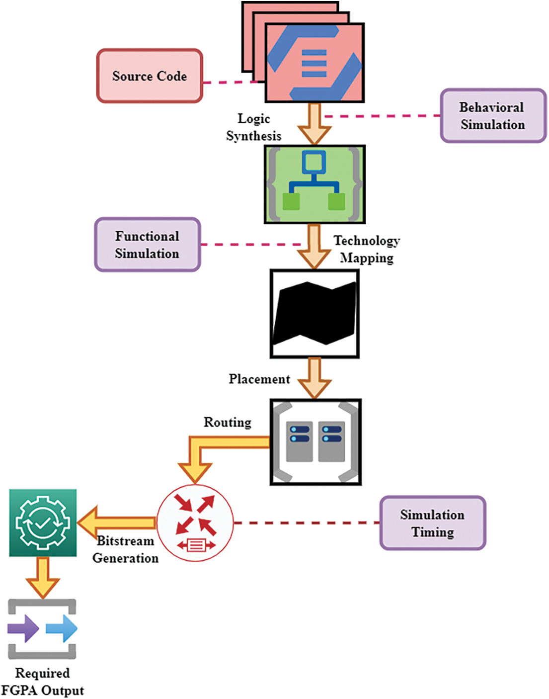
Figure 1: Design procedure of FPGA
These are the most common and essential steps in the FPGA design process, starting with source code. One of the most important factors in creating an optimized digital circuit with FPGA is EDD tools. FPGA devices are used to implement the method or circuit described by data Input in this flow. Based on the level of complexity of the design, there are two standard approaches to specifying FPGA designs: HDL and schematic-based. FPGA designers primarily use high-definition language (HDL) design entry for more complex and computationally demanding algorithms, such as technology mapping. Once the design has been specified in HDLs or logic synthesis, the designer must verify logically correct. Simulated functional and behavioral is used to accomplish this by technical mapping using functional simulation. In general, FPGA designs placement is critical. This directly impacts the routing technique and effectiveness of a design on an FPGA. The placement algorithms can be grouped under the term routing with timing-driven. It is the final step in the design process before producing the bitstream to program the FPGA. Prefabricated resources like wire segments and multiplexers are required for FPGA routing, which is time-consuming.
For the next two iterations, transition and simple arithmetic operations are applied to the scale factor from read-only memory (ROM) to obtain the component at a time
FPGA delays are considered during timing simulations to ensure that the design is logically correct. The final step in the FPGA proposed design is to generate a bit stream and download the resulting bit file.
3.2 Framework of FPGA-DA Implementation
FPGA-based signal processing methods that work with both signal processing signals. Using (fast Fourier transform) FFT, this card provides the ability to speed up and test real-time process control design concepts. The new system image analysis kit dramatically reduces computation costs and facilitates the overall design process, making it more efficient.
After initializing all input and output devices on an FPGA-DA given in Fig. 2, the communication systems methods begin to operate. The timer can be applied to analog data is then converted into digital data and stored in the internal memory by the ADC. The output of this stage is a noise-free analog signal, which is obtained by retrieving and processing the digital signal on the FPGA and synthesizing it on the EDD interface. A comparison is made between this analog signal and the previous analog signal to see if any noise has been removed. If the unwanted errors have been eliminated, the signal is transferred to the screen. The compared signal is reprocessed and synthesized if there is no change, it is sent to the signal port. After initializing all input and output devices on an FPGA-DA given in Fig. 2., the communication systems methods begin to operate. The timer can be applied to analog data is then converted into digital data and stored in the internal memory by the ADC. The output of this stage is a noise-free analog signal, which is obtained by retrieving and processing the digital signal on the FPGA and synthesizing it on the EDD interface. A comparison is made between this analog signal and the previous analog signal to see if any noise has been removed. If the unwanted errors have been eliminated, the signal is transferred to the screen. The compared signal is reprocessed and synthesized if there is no change, it is sent to the signal port.
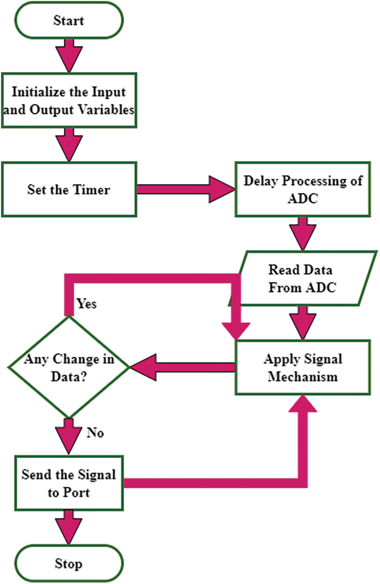
Figure 2: Flowchart for FPGA-DA framework
The above-stated Eq. (2) denotes the largest non-negative number
Conclusions drawn from this paper show that FPGAs have many advantages over general-purpose microcontrollers in real-time applications, such as in this paper’s FPGA-DA system where VLSI signals and high-speed peripherals are used.
For the design and efficient implementation of an FPGA, where resources are extremely limited, matrix multiplication has been particularly challenging. Three performance metrics are commonly used to evaluate FPGA-based designs: frequency (transmission delay), location, and energy. FPGA fixed-point implementations are a popular choice because of their speed and low power consumption. Furthermore, a fixed-point matrix multiplier unit frequently requires less silicon in an FPGA or ASIC than its suspended counterpart.
A set of low
When the low pass and high pass filters are down analyzed, their outputs contain the low-frequency signals of the original signal, which are called approximate parts, and the high-frequency components, which are highly textured parts like edges of the original signal, which are mentioned in detail from the above Fig. 3. The degradation level computations are evenly distributed between all stages in a one-to-one plotted structure. One stage performs computations for levels one through one, while subsequent stages perform computations for levels two through eight, with levels nine through twelve being handled by the final stage recursively.
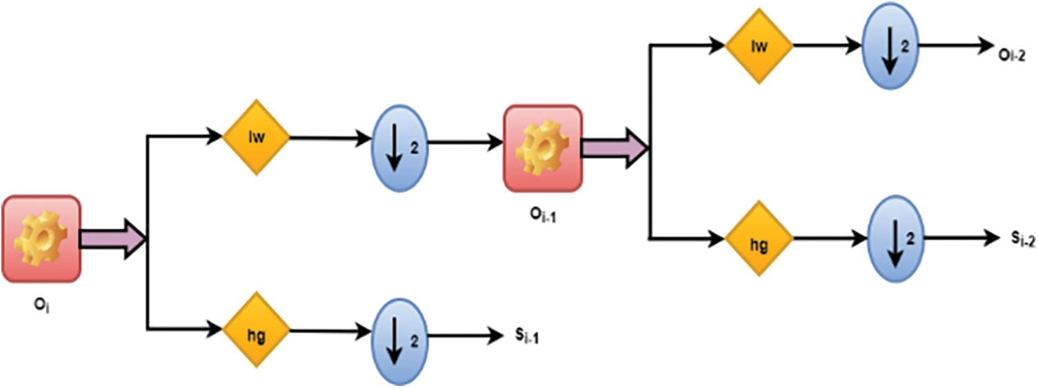
Figure 3: Signal processing in FPGA
Latency and portion have been used as performance indicators for FPGA designs. Energy efficiency and power dissipation have become increasingly important as portable mobile devices have increased in the past few years. Several components in FPGA devices use significant amounts of power, and the configurable connections are responsible for a large portion of this power consumption.
Precisely defined dilations and interpretations of the analyzer’s function, known as a wavelet, represent a signal in the discrete wavelet transform. Generally, basis functions are used in the most common form of the DWT, which uses a relational grid. From the wavelet function, researchers can derive the following equations for the generation of wavelets:
From the equation as mentioned above (5) coarse and fine expansion coefficients
Two patterns dominate the ordering of the coefficients after filtering: one that acts as a regularization term like a time series, and the other that helps bring out the complete details of the data. In the AES algorithm, the DWT is computed at multiple configurations using a space representation convolution for low-pass
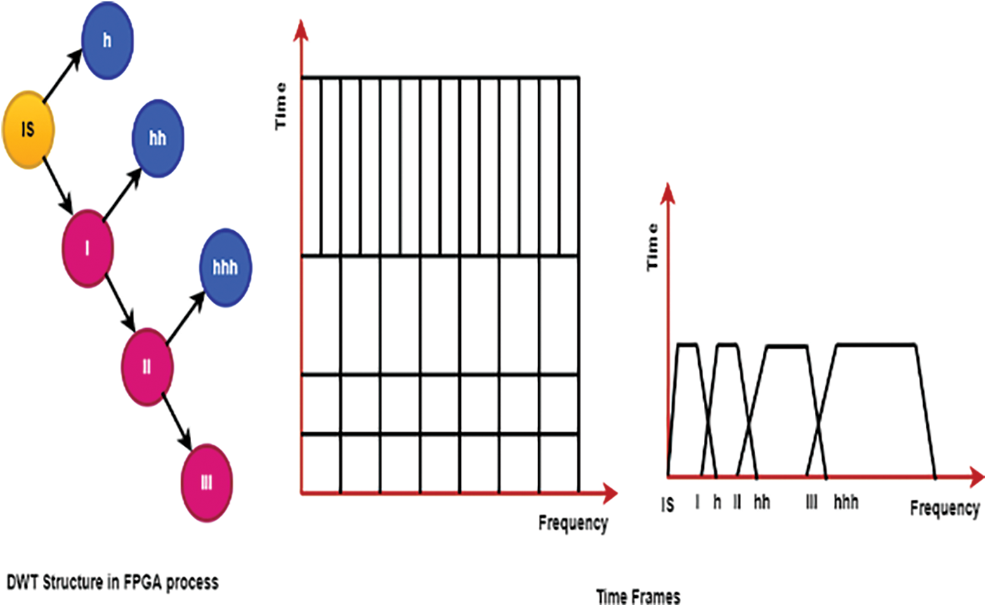
Figure 4: DWT process in FPGA-DA
The VLSI based signal processing has been filled with a weighted average
Based on the above Eq. (7), a high-pass and a low-pass filter connected with limits
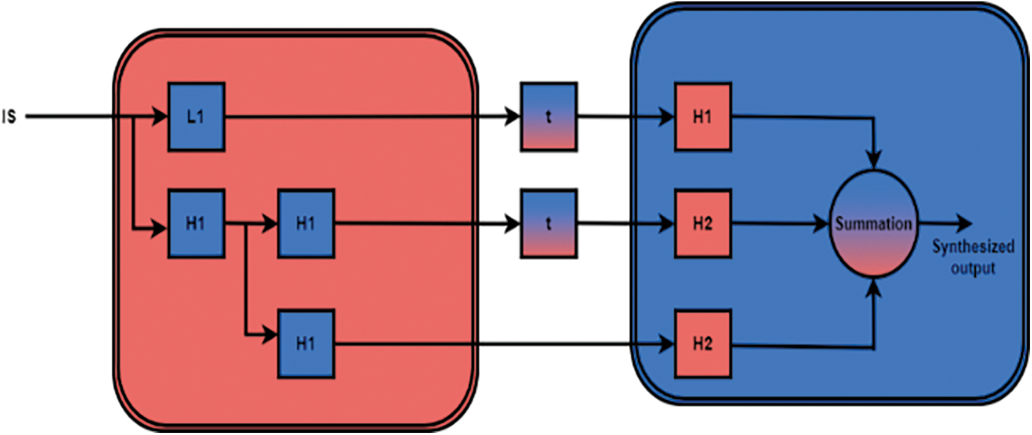
Figure 5: Framework of FPGA-DA using DWT Process
Additionally, the control signal is a synthetic test message with additional noise. Filtering parameters can be calculated based on the various noise power and use the thresholding methodology on the selected features because it is starting to use that the vast majority of the noise is encapsulated within them. Using the soft thresholding method called widespread threshold calculated using below equation,
There are indeed additional noises
In the wavelet transform field, nonlinear edge detection of detail coefficients is called wavelet compression performed to identify. The wavelet transform is used to improve the image quality of the signal by dividing it into a small number of coefficients and then applying an adaptive threshold procedure to each one. Finally, all these are summed to get a synthesized output.
For an accurate assessment of the filtering abilities, different analysis functions reflected different, and levels of noise
3.4 AES Algorithm Process in FPGA-DA
As a result of the nonlinear transformation, it is possible to perform nonlinear sector is known on the training data by simply using a linear higher dimensional space to separate the points in the training dataset. VLSI can use nonlinear mappings unique mathematical relationships to as advantages, and the algorithm is explained below,
Algorithm 1: AES algorithm for DSP
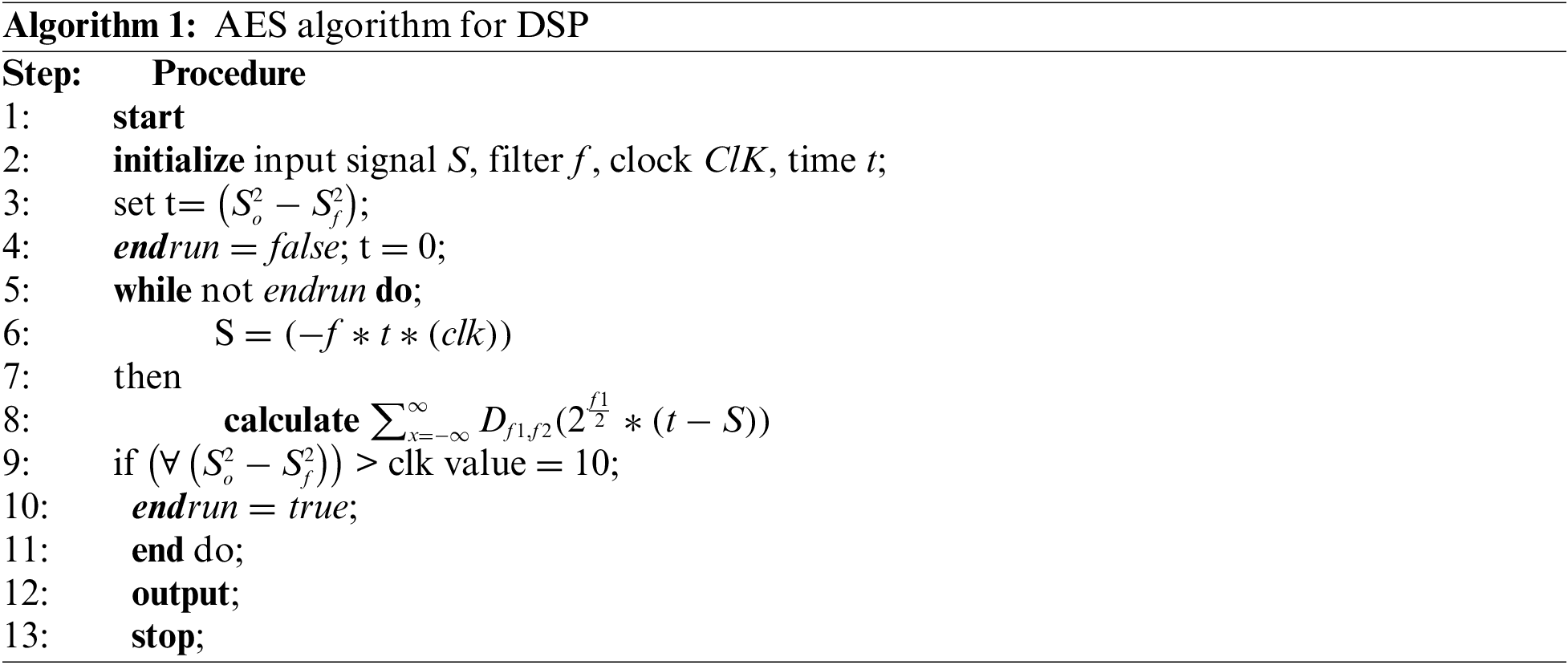
This methodology can regulate learning machine complexity, including through a structural mathematical point of view from the above algorithm (1). The inputs are one of the reasons for AES success. In a statistical framework, this principle can regulate the training machine’s complexity and define the upper limits of its generalization ability. As an alternative, our design employs AES stages in addition to the ten stages of the AES itself to produce transmission stages with clock signal
3.5 ANN Process in FPGA-DA Framework
Programmable digital signal processors are used to meet a common goal of system adaptability. Even though these platforms allow for flexible implementation thanks to programming interfaces and significant savings in performance and power efficiency, application developers and compilers must adapt their processing approach to the computing resources available on these platforms.
It can be seen from the Fig. 6 above that the degree to which inputs from training examples or classification methods resemble sample data is used to calculate an appropriate neural network for this input VLSI based signal. ANNs use primary source of information of neural networks. An ANN neuron has always processed every single piece of data, and the weights of nodes where classification is expected are shown in a shaded area. For each significant amount of state information, the convolution layer has one node and a process to calculate the weighted sum of the sources. Neural networks contain entropy functions with outputs that deviate from the neuron’s axis of symmetry. If users consider all of these factors, they get an output that is either positive or negative (either 1 or >1), depending on the model’s weighting. FPGA-DA area and computation time can be reduced by halving the number of iterations and computing all rotational directions in advance. In addition, the proposed architecture is highly customizable and can be extended to higher levels of precision. When comparing the proposed FPGA-DA to other unfolded architectures, it is understood that the number of stages is reduced while unwanted signals are eliminated.
Figure 6: ANN in FPGA-DA
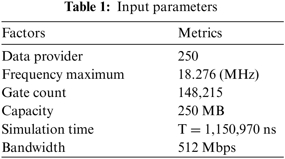
An AES algorithm based on training instances is used to calculate the core’s signal processing method. FPGA-DA outcomes can be tested with the MATLAB. The suggested FGPA-DA with DWT and AES system prototype was built on a virtex 6 FPGA with the XC6VCX75T package using Xilinx tools. However, it is an experimental method on the topic. It can be used to understand its primary properties, such as the number of clock cycles required to arrive at a workable solution, clock frequency, and device utilization. To achieve this goal, here focus on creating an RBF-DWT prototype and that the same process can be easily applied to other DWTs. Tab. 1 depicts scene elements in a detained setting.
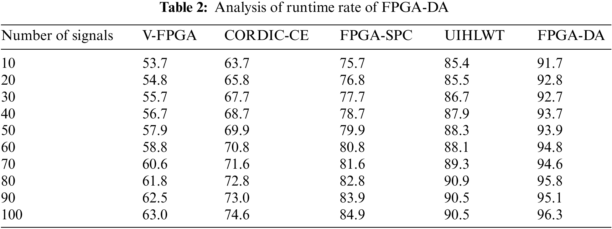
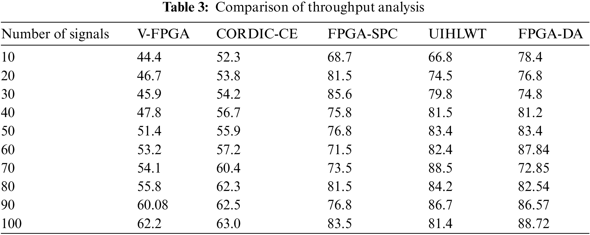
This setup is used to test the proposed system’s FPGA-DA efficacy under real-world conditions, using the parameters optimization comparison, cost savings, improved runtime effectiveness rate, throughput rate, and reliability analysis as shown in Tabs. 2 and 3, respectively. As part of the digital architecture, a method developed to perform two lifting steps with 9 by 7 filtering and five pipeline stages to reduce the computation time.
Many important aspects to consider, such as alternatives, movement, and cost assessments, are part of the problem-solving space when solving multi-objective optimization problems. In FPGA-DA designing an ASIC is a way to reduce the cost and size of an integrated device, product, or system by integrating individual elements and their features into a single element is calculated using optimizing parameter mentioned in Eq. (3). Logical circuit timing optimization is a critical step in synthesizing logic circuits. The majority of existing research data is based on various computational intelligence techniques mentioned in Fig. 7. A design compiler (DC) algorithm is being used to improve the duration of the same circuit using settings and constraints.
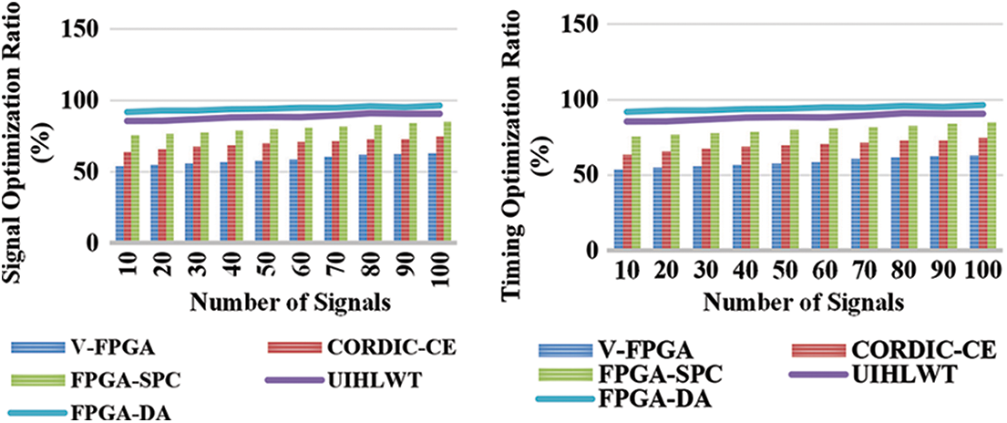
Figure 7: Comparing optimization of FPGA-DA with other techniques
4.2 Cost Savings Techniques in FPGA-DA
It is possible to have a digital signal or a sustained signal because the domain of a continuous signal is time, e.g., a linked timeframe of the reals. The term prolonged signal refers to a constant amplitude and time obtained using Eq. (6). Here, FPGA-DA saving of cost (SoC) is compared with other traditional methods such as V-FPGA, FPGA-SPC, 1-D WDC-LS, CORDIC-CE illustrated in Fig. 8. The output achieved is calculated between constant time and SoC analyzed above.
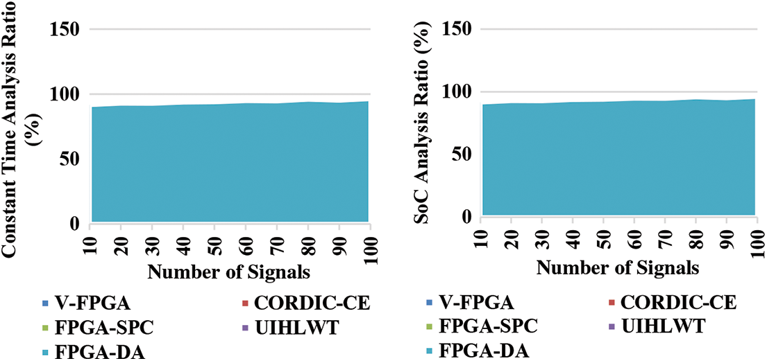
Figure 8: Cost saving analysis
4.3 Runtime Effectiveness Rate Comparisons
In our proposed system, regardless of the processing delay, samples that are being analyzed (input) and generated (output) continuously can be processed (or generated) as part of an actual digital signal computation process are calculated in Eq. (8). AES algorithms’ runtime efficiency in FPGA is critical to consider in conventional methods. Taking too long to solve a problem incurs additional costs and prevents the signal processing of valuable time in the table as mentioned above 1. AES algorithm efficiency is defined as a computational cost that falls within a predetermined range. According to this definition, satisfactory means that it can be run on an available virtual machine in the allotted time or space, obtained from Eq. (9), generally as a function of the largest connected component.
4.4 Throughput Rate Comparison
Although throughput is typically measured in bits per second (bps), it can be measured in data packets per second (p/sec) or time slots mentioned in Tab. 2. In a network, the data rates delivered to all devices are summed up as the system throughput to calculate aggregate analysis of throughput using Eq. (10). A signal can be transferred in a given amount of time, and it is the network’s or transmission medium’s capacity to carry signals from one medium to another in FPGA-DA. A network, interface, or channel’s data transmission capacity is measured during a given time. This FPGA-based signal processing card can handle digital and analog signals. Using FFT provides the ability to speed up and test real-time signal processing designs. With the new scheme signal processing kit, simulation time is drastically reduced, and the design process is generally simplified.
4.5 Reliability Analysis Comparison of FPGA-DA with Other Methods
Based on Eq. (5), digital signal processing (DSP) algorithms can be implemented on FPGAs, and this paper presents a list of fundamental issues with implementing DSP algorithms on FPGAs. Knowing the sampling and computation rates of various applications is important to determine how they impact our FPGA-DA design shown in the Fig. 9. Various analysis functions wavelets and noise addition levels are used to test the filtering performance on the noisy data signal to get the most accurate results by defining the root of the square.
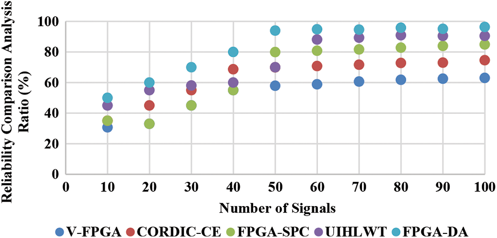
Figure 9: Reliability analysis comparison
By halving the number of iterations and computing all rotational directions in advance, here present architecture of FPGA-DA that reduces both its surface area and computation time. The proposed architecture is highly configurable and extendable to higher precision as well. Comparison of proposed FPGA-DA with other unfolded architectures in the literature shows that the number of stages is reduced while unwanted signals are eliminated.
Over other traditional approaches, new hardware architecture for the AES algorithm has been proposed as (FPGA-DA) and compared to two AES hardware structures, iterative repetition and transmission approach. Using an FPGA, researchers can implement the structure in the real world. Here there is increased throughput by approximately 88.72%. Furthermore, it has a superior throughput advantage of 90.2% over the iterative looping AES structure; however, the area is 3.5 times larger than the sequential looping structure. Rather than evaluating 16 bytes of data simultaneously with all of the hardware requirements, the reordering of bytes streamlines the evaluation in parallel. Partitioning the AES into sub-blocks with intermediate buffers in between is another important feature, as it creates an extensive parallel processing structure for all AES blocks. DWT-based learning on a digital architecture has been discussed in this paper and is an example of how it is implemented on an FPGA device. In FPGA-DA, it is possible to improve the results obtained significantly. Because of this, slightly modified versions may exist that originate initialized operating at higher clock frequency bands. In the spirit of immediately preceding neural processors, future work will solve this challenge by integrating a general-purpose baseband processor and a learning controller module on the same chip.
Acknowledgement: The authors extend their appreciation to King Saud University for funding this work through Researchers Supporting Project number (RSP-2021/387), King Saud University, Riyadh, Saudi Arabia.
Funding Statement: This work was supported by King Saud University for funding this work through Researchers Supporting Project number (RSP-2021/387), King Saud University, Riyadh, Saudi Arabia.
Conflicts of Interest: The authors declare that they have no conflicts of interest to report regarding the present study.
References
1. S. H. Mirfarshbafan, M. Shabany, S. A. Nezamalhosseini and C. Studer, “Algorithm and VLSI design for 1-bit data detection in massive MIMO-OFDM,” IEEE Open Journal of Circuits & Systems, vol. 1, pp. 170–184, 2020. [Google Scholar]
2. A. Palchaudhuri and A. S. Dhar, “Design and automation of VLSI architectures for bidirectional scan-based fault localization approach in FPGA fabric aware cellular automata topologies,” Journal of Parallel & Distributed Computing, vol. 130, no. 3, pp. 110–125, 2019. [Google Scholar]
3. A. A. Yazdeen, S. R. Zeebaree, M. M. Sadeeq, S. F. Kak, O. M. Ahmed et al., “FPGA implementations for data encryption and decryption via concurrent and parallel computation: A review,” Qubahan Academic Journal, vol. 1, no. 2, pp. 8–16, 2021. [Google Scholar]
4. G. D. P. Stanchieri, A. D. Marcellis, E. Palange and M. Faccio, “A true random number generator architecture based on a reduced number of FPGA primitives,” AEU-International Journal of Electronics & Communications, vol. 105, no. 3, pp. 15–23, 2019. [Google Scholar]
5. A. Farzana, H. Arshadh, J. Ganesan and M. Muthukumaran, “High-performance VLSI architecture for advanced QPSK modems,” Asian Journal of Applied Science & Technology, vol. 3, pp. 45–49, 2020. [Google Scholar]
6. M. A. Hajjaji, M. Gafsi, A. B. Abdelali and A. Mtibaa, “FPGA implementation of digital images watermarking system based on discrete HAAR wavelet transform,” Security & Communication Networks, vol. 2019, no. 1, pp. 1–17, 2019. [Google Scholar]
7. Y. H. Chen, S. W. Chen and M. X. Wei, “A VLSI implementation of independent component analysis for biomedical signal separation using the CORDIC engine,” IEEE Transactions on Biomedical Circuits & Systems, vol. 14, no. 2, pp. 373–381, 2020. [Google Scholar]
8. V. Pathak, S. J. Nanda, A. M. Joshi and S. S. Sahu, “VLSI implementation of the anti-notch lattice structure to identify exon regions in eukaryotic genes,” IET Computers & Digital Techniques, vol. 14, no. 5, pp. 217–229, 2020. [Google Scholar]
9. V. Bevara and S. K. Pradyut, “VLSI implementation of high throughput parallel pipeline median finder for IoT applications,” Sādhanā, vol. 45, no. 1, pp. 1–5, 2020. [Google Scholar]
10. V. Leon, S. Xydis, D. Soudris and K. Pekmestzi, “Energy-efficient VLSI implementation of multipliers with double LSB operands, IET circuits,” Devices & Systems, vol. 13, no. 6, pp. 816–821, 2019. [Google Scholar]
11. V. Sharma and A. M. Joshi, “VLSI implementation of reliable and secure face recognition system,” Wireless Personal Communications, vol. 3, no. 1, pp. 1–13, 2021. [Google Scholar]
12. D. Datta and H. S. Dutta, “High-performance IIR filter implementation on FPGA,” Journal of Electrical Systems & Information Technology, vol. 8, no. 1, pp. 1–9, 2021. [Google Scholar]
13. D. Datta, P. Mitra and H. S. Dutta, “FPGA implementation of high-performance digital down converter for software-defined radio,” Microsystem Technologies, vol. 2, pp. 1–10, 2019. [Google Scholar]
14. S. Afifi, H. GholamHosseini and R. Sinha, “FPGA implementations of DWT classifiers: A review,” SN Computer Science, vol. 1, no. 3, pp. 1–17, 2020. [Google Scholar]
15. S. H. Mirfarshbafan, A. Gallyas-Sanhueza, R. Ghods and C. Studer, “Beamspace channel estimation for massive MIMO mmWave systems: Algorithm and VLSI design,” IEEE Transactions on Circuits & Systems, vol. 67, no. 12, pp. 5482–5495, 2020. [Google Scholar]
16. D. Gutierrez-Galan, J. P. Dominguez-Morales, A. Jimenez-Fernandez, A. Linares-Barranco and G. Jimenez-Moreno, “OpenNAS: Open source neuromorphic auditory sensor HDL code generator for FPGA implementations,” Neurocomputing, vol. 436, no. 11, pp. 35–38, 2021. [Google Scholar]
17. B. N. M. Kumar and R. H. Gangappa, “Low area VLSI implementation of CSLA for FIR filter design,” International Journal of Intelligent Engineering & Systems, vol. 12, no. 4, pp. 90–99, 2019. [Google Scholar]
18. K. L. Du and M. N. S. Swamy, “Neural network circuits and parallel implementations,” in Proc. Neural Networks & Statistical Learning, London, UK, pp. 829–851, 2019. [Google Scholar]
19. C. A. Lúa, S. Di Gennaro, A. N. Guzman, S. Ortega-Cisneros and J. R. Domínguez, “Digital implementation via FPGA of controllers for active control of ground vehicles,” IEEE Transactions on Industrial Informatics, vol. 15, no. 4, pp. 2253–2264, 2019. [Google Scholar]
20. T. Bonny, R. Al Debsi, S. Majzoub and A. S. Elwakil, “Hardware optimized FPGA implementations of high-speed true random bit generators based on switching-type chaotic oscillators,” Circuits Systems, & Signal Processing, vol. 38, no. 3, pp. 1342–1359, 2019. [Google Scholar]
21. T. Zhan, S. Z. Fatmi, S. Guraya and H. Kassiri, “A Resource-optimized VLSI implementation of a patient-specific seizure detection algorithm on a custom-made 2.2 cm$^2$ wireless device for ambulatory epilepsy diagnostics,” IEEE Transactions on Biomedical Circuits & Systems, vol. 13, no. 6, pp. 1175–1185, 2019. [Google Scholar]
22. R. B. Chaurasiya and R. Shrestha, “Fast sensing-time and hardware-efficient eigenvalue-based blind spectrum sensors for a cognitive radio network,” IEEE Transactions on Circuits & Systems, vol. 67, no. 4, pp. 1296–1308, 2019. [Google Scholar]
23. S. Rakesh and K. V. Grace, “A comprehensive review of the VLSI design performance of different parallel prefix adders,” Materials Today: Proceedings, vol. 11, no. 1, pp. 1001–1009, 2019. [Google Scholar]
24. H. Hikawa, “Hardware self-organizing map based on digital frequency-locked loop and triangular neighborhood function,” IEEE Transactions on Circuits & Systems, vol. 68, no. 3, pp. 1245–1258, 2021. [Google Scholar]
25. J. L. Contreras-Hernandez, D. L. Almanza-Ojeda, S. Ledesma and M. A. Ibarra-Manzano, “Motor fault detection using quaternion signal analysis on FPGA,” Measurement, vol. 138, no. 7, pp. 416–424, 2019. [Google Scholar]
26. V. N. Reddy, V. Lavanya and B. Kiranmai, “Radar pulse compression waveform generation using FPGA implementation,” i-Manager’s Journal on Digital Signal Processing, vol. 7, no. 2, pp. 40, 2019. [Google Scholar]
27. P. J. Ahamed and M. A. Haseeb, “Implementation of digital IIR filter design based on field-programmable gate array,” Materials Today: Proceedings, vol. 45, pp. 2573–2577, 2021. [Google Scholar]
28. P. C. Ch and J. B. Seventline, “VLSI implementation of distributed arithmetic-based block adaptive finite impulse response filter,” Materials Today: Proceedings, vol. 33, no. 2, pp. 3757–3762, 2020. [Google Scholar]
29. P. Chen, J. T. Lan, R. T. Wang, N. M. Qui, J. C. J. S. Marquez et al., “High-precision PLL delay matrix with overclocking and double data rate for accurate FPGA time-to-digital converters,” IEEE Transactions on Very Large Scale Integration (VLSI) Systems, vol. 28, no. 4, pp. 904–913, 2020. [Google Scholar]
Cite This Article
 Copyright © 2023 The Author(s). Published by Tech Science Press.
This work is licensed under a Creative Commons Attribution 4.0 International License , which permits unrestricted use, distribution, and reproduction in any medium, provided the original work is properly cited.
 Downloads
 Citation Tools