
 Submit a Paper
 Propose a Special lssue
 Open Access
ARTICLE

2D MXene Ti3C2Tx Enhanced Plasmonic Absorption in Metasurface for Terahertz Shielding
1 Faculty of Electrical Engineering, College of Engineering, Al Ain University, Al Ain, 64141, UAE
2 Department of Electrical Engineering, Durham University, Durham, UK
3 Department of Electrical Engineering, Baluchistan University of Technology and management sciences, Quetta, Pakistan
4 Institute of Digital Signal Processing, Universitat Duisburg Essen, Duisburg, Germany
* Corresponding Author: Zaka Ullah. Email:
Computers, Materials & Continua 2023, 75(2), 3453-3464. https://doi.org/10.32604/cmc.2023.034704
Received 25 July 2022; Accepted 23 September 2022; Issue published 31 March 2023
 View Full Text
 Download PDF
Abstract
With the advancement of technology, shielding for terahertz (THz) electronic and communication equipment is increasingly important. The metamaterial absorption technique is mostly used to shield electromagnetic interference (EMI) in THz sensing technologies. The most widely used THz metamaterial absorbers suffer from their narrowband properties and the involvement of complex fabrication techniques. Materials with multifunctional properties, such as adjustable conductivity, broad bandwidth, high flexibility, and robustness, are driving future development to meet THz shielding applications. In this article, a theoretical simulation approach based on finite difference time domain (FDTD) is utilized to study the absorption and shielding characteristics of a two-dimensional (2D) MXene Ti3C2Tx metasurface absorber in the THz band. The proposed metamaterial structure is made up of a square-shaped array of MXene that is 50 nm thick and is placed on top of a silicon substrate. The bottom surface of the silicon is metalized with gold to reduce the transmission and ultimately enhance the absorption at 1–3 THz. The symmetric adjacent space between the MXene array results in a widening of bandwidth. The proposed metasurface achieves 96% absorption under normal illumination of the incident source and acquires an average of 25 dB shielding at 1 THz bandwidth, with the peak shielding reaching 65 dB. The results show that 2D MXene-based stacked metasurfaces can be proven in the realization of low-cost devices for THz shielding and sensing applications.Keywords
Terahertz metamaterial absorber technology is expected to have a wide range of cutting-edge applications in the field of THz plasmonics. Plasmonic surface waves propagating at metal-dielectric interfaces provide an efficient method of realizing terahertz optoelectronic devices for biosensing [1] and EMI shielding applications [2]. The extremely delocalized nature of terahertz surface plasmonic waves has previously been a source of concern. Although recent discoveries have shown that the confinement of plasmonic waves and their propagating mechanism in the terahertz band can be manipulated by designing surface structures with different material shapes [3].
The most common technology for terahertz absorbers are metamaterials, also known as artificially engineered magnetic conductors. Metamaterials are highly conductive and of particular shaped sub-wavelength periodic structures [4]. Metamaterials achieve absorption at a specific terahertz frequency utilizing intrinsic loss with the aid of complex geometrical design and their control over dielectric permittivity [5] and conductivity properties [6]. However, single-mode metamaterials have the limitations of narrowband operating bandwidth [7] and low absorption [1], resulting in lower absorption efficiency, thus reducing performance [6]. Incorporating numerous resonant structures in metamaterial is an excellent way to improve the overall absorption i.e., broadband [8] and multilayer stack structure [9] has been reported in the spectral range from terahertz to optical regime [2]. In metamaterial technology, mainly frequency selective surfaces (FSS) are employed for EMI shielding applications. In [10], a compact ultra-wideband FSS is demonstrated for shielding purposes in the microwave region, where the results suggest that the designed FSS has a stable performance with different polarization incidence. In another study [11], a metamaterial-based on thin graphene sandwiched layers was studied for EMI shielding. The graphene in the metamaterial provides tunability along with a 10 dB enhancement in shielding effectiveness. In addition, a triple band split ring resonator (SRR) metamaterial has been analyzed for shielding and stealth applications [12]. The authors successfully achieved shielding effectiveness greater than 40 dB at C and X bands by utilizing a double E-shaped symmetric array in the SRR metamaterial. The study in [13], explores the magnetic shielding properties of Fe-Ni alloy through numerical simulations. Nonetheless, most of the metamaterial terahertz absorbers have less absorption efficiency at the operating bandwidth [14]. It is challenging to acquire an appropriate absorption intensity and a broad absorption bandwidth range.
THz shielding is also excellent in 2D materials, which can effectively combine the intrinsic properties [15] with the structural qualities of 2D materials [16]. In the terahertz region, these innovative 2D structures can maximize impedance matching conditions and enable multiple terahertz scattering responses, resulting in high absorption efficiency with active control of shielding performance [17]. MXenes are a new family of 2D materials exhibiting high conductivity [18], high strength [19], ultra-thinness [15], and tunable electromagnetic responses [20] have shown better performance in the terahertz region [19]. The better performance has encouraged researchers to realize broadband terahertz absorbers for shielding applications. Moreover, a monoatomic layer is incapable of absorbing maximum incident terahertz radiation [21], whereas large stacked films of 2D material pose impedance mismatching [22]. Therefore, it is essential to construct 2D material-based metamaterials that may have the benefit of tunability, i.e., to adjust the dielectric permittivity and magnetic permeability to fully utilize the advantages of 2D materials [1].
In recent years, various studies have shown the excellent response of MXene to electromagnetic (EM) waves. In ref [23], broad optical absorption at the terahertz range was investigated using a combination of MXene and hydrogel sheet, acquiring a 45.3 dB peak shielding efficiency (SE) at the bandwidth range (0.2–2 THz). Choi et al. [24] experimentally demonstrated the shielding performance of thin film MXene drop cast on slotted nanoantennas. The interface between the nanoantenna slots and MXene film enhances the EMI at the THz region by three orders of magnitude, which in turn increases the shielding efficiency. The total average SE of 20 dB is realized with the coupled method with the MXene film thickness of 400 nm. In other study [25], MXene-based metamaterial sponges are reported to achieve high absorption. The authors utilized the large pore size of the foam with 2D metallic MXene flakes to increase the absorption at the THz range (0.3–1.65 THz). However, the SE could be reached at 40 dB when the mass of the MXene is 6.6 mg with a sufficiently high thickness of 10 mm. In [26], hybrid MXene and graphene oxide films are experimentally analyzed for stealth purposes in the THz band. The effective coupling of a 4 mm thick MXene layer with graphene oxide achieves 37 dB of reflection loss at 2 THz resonance frequency. The increase in the MXene thickness improves the absorption property, which enhances the shielding ability. The absorption mechanism of MXene film gold metamaterial structure is numerically investigated for shielding applications [27], where the thick layer Ti3C2Tx couples far-field energy with the help of gold nanorods. The coupling in the cavity interface between the MXene and gold produces high absorption and can be tuned by changes in the incident source polarization or geometric parameters. The effect of terahertz modulation is studied using strain-sensitive MXene on a flexible substrate [28]. The study shows that MXene conductivity can be tuned by using tensile strength on the film, whereas 80% absorption is achieved at the THz band. In the above studies, researchers use different devices and films for shielding purposes with thick material layers at a specific resonance frequency. Therefore, it is necessary to model ultra-thin metasurface devices which can not only have the tuning ability to control the optical characteristics at the terahertz regime but also ease of fabrication and low cost.
In this article, a simulation study was conducted on metasurface absorbers based on MXene nanomaterial for the first time to explore the EMI shielding capability in the terahertz region. The proposed metasurface achieves strong resonance absorption at a bandwidth of 1–3 THz with the highest peak value of 96% absorption resonance wavelength. The shielding performance is calculated from the strength of absorption in the structure and the effective field coupling between the adjacent elements. The maximum EMI shielding in the operational bandwidth (1–3 THz) reaches 60 dB, which is highly effective in stealth and shielding applications. Moreover, this study provides insight into the tunable resonance behavior when the MXene properties are changed either through the incident source angle or the change in layer thickness.
2 Simulation Design Methodology
In this section, the design and simulation methodology of MXene-based terahertz metasurface are discussed. Generally, super absorber metamaterial designs are based on metal constituents. In this study, a hybrid scenario of MXene and metal constituents is considered for broadband absorption. The motivation behind using MXene periodic structure is the feasibility of fabrication. Using thin MXene films can easily produce surface patterns of metasurface shapes (sharp corners, rounded edges, slanted sides), whereas metallic metamaterial involves complex fabrication procedures and high cost [8]. The schematics of the MXene-based periodic metamaterial are presented in Fig. 1. The design structure is comprised of a symmetric array of MXene squares on the top of the substrate. The thickness of MXene arrays is hm = 50 nm, which is a stack of multilayer 2D MXene layers. The dimensions of the square shape are px (length and width) are 2 µm. The array elements are equally spaced with the adjacent distance between the two elements being d = 1 µm. It should be noted that the gap space between the elements should be kept small because it can provide the coupling of the plasmon resonance field. The base substrate for the metasurface absorber is a high resistive dielectric substrate Si/SiO2, which is periodic along the x-axis and y-axis and can readily sustain plasmonic resonance on the surface of the suggested shape. The SiO2 acts as a dielectric spacer, which helps in reducing the effect of quantum tunneling [29]. Silicates have distinct crystal forms. Depending on the relative orientation of silicon and silicon dioxide crystals, atoms near the interface can adopt various shapes. Some interfaces facilitate tunneling, while others discourage it. Therefore, reducing tunneling at this junction will be crucial for improving absorption [30]. Finally, the bottom surface of the metamaterial is metalized with a 5 nm gold layer to block the transmission of the absorbed terahertz energy and enhance the absorption of MXene metamaterial.
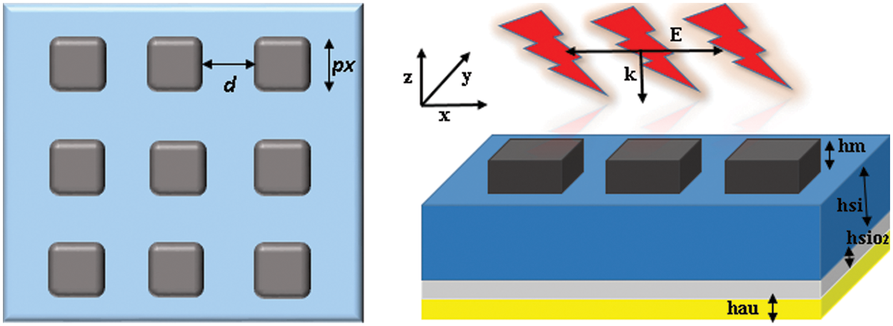
Figure 1: Schematic illustration of MXene terahertz metamaterial absorber, d is the adjacent spacing between the array elements. hsi = 0.2 µm, hsio2 = 40 nm, and hau = 35 nm denotes the thickness of the silicon substrate, silica, and gold reflector layer respectively. The TM polarized incidence source has a propagating vector ‘k’ directed normally towards the metasurface structure
The metamaterial structural size is large enough to sustain surface plasmons resonance when excited by terahertz incident source wave under different incident angles. The designed model is numerically simulated by the FDTD method using computer simulation technology (CST) software. High computing resources are required when it comes to the simulation of nanomaterials in the geometrical structure because of the high mesh grid along the array surface. Here we keep the mesh grid size of 2 nm along the vertical and horizontal axis. For the simulation setup, periodic boundary conditions (PBC) are applied along the horizontal plane (x-axis and y-axis) and perfectly matched layers (PML) are applied along the vertical axis to capture all the incident energy from the source at the surface of the metasurface. The proposed structure is excited with transverse magnetic (TM) linearly polarized incident plane waves having a polarization angle ‘θ’ from the top surface of the MXene metasurface at 1 to 4 THz range.
The MXene Ti3C2Tx layer is modeled based on published experimental data to analyze the analytical dependence of relative dielectric permittivity using the Drude-Lorentz formula. So far, two research articles [16,24] report the relative dielectric permittivity through experimentation of MXene films. Although none of the research articles provide an analytical expression for the complex permittivity in the terahertz range [4]. This step is very crucial in the simulation of such 2D materials because the performance of the metamaterial depends on the material properties such as dielectric permittivity, refractive index, and conductivity. Therefore, the optical and electrical properties are extracted from the literature for modeling MXene metamaterial.
Based on the data retrieved from the experimental investigation published in [16], the parameters are calculated using Drude-Lorentz spectral dispersion of relative dielectric permittivity for a 50 nm thick MXene film. The expression of the Drude-Lorentz model for MXene [4] is given by
ωp = 4.21 × 10¹⁴ rad/s denotes the plasma frequency for 50 nm thick MXene sheet, scattering loss is γ = 8.65 × 10¹⁴ rad/s and ε1 = 6.0, ε2 = 3.0, ε3 = 0.2 are the fitting parameters. MXene exhibits very high electrical conductivity ~2000 S/cm in a free space environment. The increase in conductivity is also dependent upon the thickness of the MXene sheet (i.e., staked layer) [31]. It is worth noting, that optical absorption depends on the refractive index of MXene at the terahertz range. According to the Kubo formalism, the mathematical expressions for refractive index and optical properties are as follows: [22,32],
where χ(ω), η(ω), ε(ω) represent the frequency susceptibility, refractive index, and dielectric constant.
Fig. 2a represents the refractive index of MXene at terahertz, as at lower frequency ranges MXene is highly refractive, but significantly decreases towards higher frequencies. The real and imaginary dielectric permittivity in Fig. 2b illustrates the highly conductive behavior in the terahertz range, as the real part of εr is negative. The EM wave absorption capability of 2D materials is largely dependent on the relative complex permittivity and permeability. Due to their good electrical conductivity and huge surface area, Ti3C2Tx sheets stack give rise to additional conductivity, which further causes the shift from mild jump migration loss of the semiconductor to the strong conductor. The black line in Fig. 2b depicts the metallic behavior; the real part of permittivity increases towards more negative values as the frequency rises, thus approving high conductivity and metal-like behavior at plasmonic frequencies.
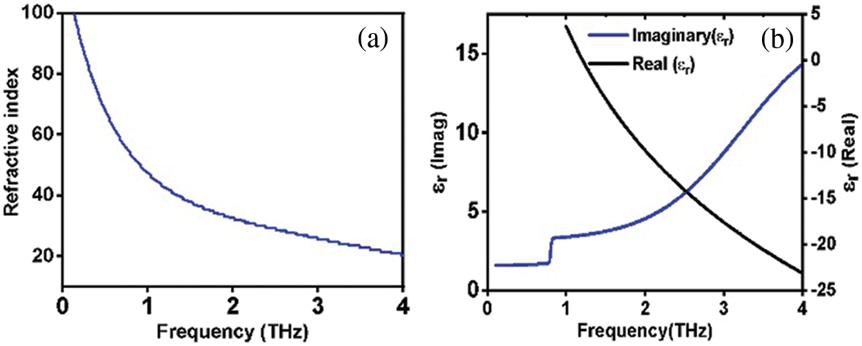
Figure 2: (a) Refractive index of MXene sheet at terahertz range with calculation from Eq. (4), (b) calculation of complex dielectric permittivity of MXene with the Drude-Lorentz model
The value of reflection loss (RL) confirms the EM wave absorption ability of the MXene metasurface. Following the transmission line theory, the RL can be computed by the correlation between the complex permittivity and complex permeability as follows: [18],
where input impedance is Zin, free space impedance is represented by Zo, d = hm is the thickness of multilayer MXene, (ɛr, μr) is the corresponding permittivity and permeability, and f is the resonance frequency of metasurface. About 90% of EM waves can be absorbed when RL < −10 dB at the resonating frequency. Fig. 3a illustrates the EM wave absorption capability of MXene metasurface with varying MXene layer thickness. Notably, it can be observed, that the metasurface exhibits the best absorbing performance with an optimal minimal reflection loss of −43 dB with a 50 nm layer thickness. Whereas decreasing the thickness of the MXene layer from 40 to 30 nm results in a low reflection loss of −30 and −25 dB, as shown in Fig. 3a. Impedance matching determines the amount of EM waves that enter the MXene metasurface, allowing for a better understanding of the EM absorption capability and is expressed by
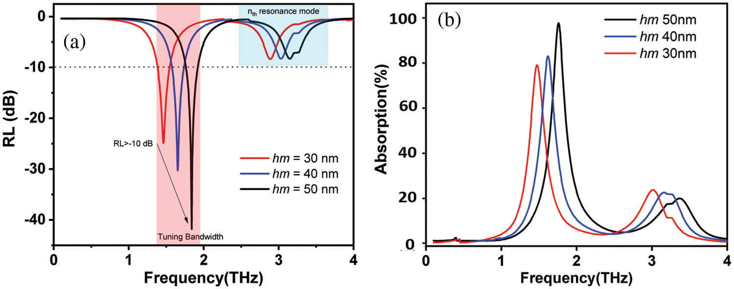
Figure 3: (a) RL of the MXene metasurface with varying MXene layer thickness, (b) spectra of absorption dependence on the MXene sheet thickness, as the thickness is varied the resonance response blue shifts with achieving higher absorption. The total resonance tuning is 0.4 THz when the thickness is varied from 30–50 nm
The absorption responses of the proposed metamaterial have been analyzed with varying thicknesses of the top MXene sheet and with a change of incidence angle. When the TM polarized terahertz waves impinge on the surface of MXene metamaterial, the striking wave activates the surface plasmon resonance at the terahertz region. The collective coupling of plasmon resonance and the incident terahertz wave provides enhanced absorption at 1–2 THz with a second harmonic resonance at 2.5–3.5 THz bandwidth. The dependence of the thickness versus absorption resonance is illustrated in Fig. 3b. The thickness of MXene materials can be varied according to design requirements and target performance. Significantly, the thickness of MXene plays an important role in the absorption of terahertz energy. The increase in the thickness changes the conductivity, which in turn amplifies the absorption features of the metamaterial. In simulation, when the thickness of MXene hm = 30 nm is selected, the metamaterial achieves absorption of 81% at 1.4 THz resonance frequency with a second harmonic at 3 THz center frequency with 30% absorption. The higher absorption achieved can be attributed to the cavity formation of MXene metamaterial as the stacked structure with different refractive index materials forms a cavity shape that acts as a confining region for the surface plasmons propagation, resulting in enhanced localized surface plasmons fields with a high strength of absorption.
When the sheet thickness is increased to 40 nm, the absorption resonance spectra shift towards higher terahertz frequencies, as shown by the blue line in Fig. 3b. The shift in resonance is because of the increased conductivity of the MXene sheet due to the increase in interlayer coupling and also better impedance matching with the incident wave energy. The absorption with a 40 nm sheet has a centered resonance frequency at 1.6 THz with 85% absorption. The 10 nm increase in the MXene thickness produces a resonance shift of 0.2 THz. Further reaching to the desired thickness, i.e., hm = 50 nm. As shown in Fig. 3b, higher absorption of nearly 95% is achieved at 1.8 THz center frequency. Apart from the resonance shifting, the bandwidth improves with an increasing thickness, which also verifies the tunable properties of MXene material. Normally, single-layered materials can achieve low optical absorption. The rise in conductivity due to the addition of more layers improves the performance.
The mechanism of absorption resonance is further studied with the change in the incidence angle of the excitation source as shown in Fig. 4a. The incoming light is a TM plane electromagnetic wave that moves in a normal direction to the surface of MXene. It has a transverse electric field on the x-axis and follows the Maxwell wave equation [32] as follows:
where ‘ω’ is the angular resonance frequency of the model, k is the plasmon propagating vector in the material medium, and σ represents the conductivity of MXene. The usage of perfectly matched layers (PML) stops all the potential field dispersion or backscattering to the metasurface physical model. The absorption is calculated from the reflection and transmission coefficients, A = 1 − R − T.
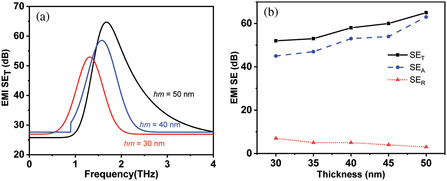
Figure 4: (a) EMI shielding was calculated from the absorption at the varying thicknesses of the MXene material. The EMI shielding dramatically rises as the sheet thickness is varied from 30 to 50 nm, the black line represents the maximum shielding performance obtained for the proposed metamaterial, (b) the total SE with pea shielding value at resonance position with varying thickness
Thanks to their exceptional conductivity, MXene 2D layers have been extensively used to model high-performance EMI shielding devices. However, to create the perfect EMI shielding materials, high permittivity and high permeability are needed due to the nature of EM waves. Our designed metasurface, which has both magnetic and dielectric components, is therefore anticipated to be very effective in EMI shielding. The total EMI shielding efficiency (SET) is equal to the absorption shielding efficiency (SEA) and reflection shielding efficiency (SER) [18,33], which is as follows,
In this case, metasurface validates the absorption dominant mechanism that contributes to the EMI shielding performance. The shielding performance of a metamaterial can be collectively determined by the electrical conductivity and thickness of the 2D material used in the metasurface structure. However, increasing the thickness of MXene to overcome the negative effect of lower conductivity can dramatically improve the shielding performance. Furthermore, the MXene structure allows multiple scattering and polarization conversion of the impinging terahertz waves, which contributes to high shielding. As a result, the patterning of MXene material in shape form could greatly improve the terahertz shielding capability. The shielding capability of the metamaterial concerning MXene thickness can be observed in Fig. 4a. The 30 nm thick MXene has significantly lower terahertz shielding with an average peak shielding of 53 dB across 1 THz bandwidth. The shielding capability for the proposed structure increases when the thickness is raised to 40 nm, i.e., SE = 57 dB. At 50 nm thickness, the peak shielding reaches 65 dB as shown in Fig. 4a, which is due to the high strength of the absorption resulting from the coupling of individual plasmonic enhancements of the array geometry. The findings in this study indicate, that the increasing absorption is the major source of the EMI SE enhancement triggered by increased MXene thickness. With varying thicknesses, the increased conductivity makes it easier to match the impedance at the absorption resonance.
When the absorption is gradually increased with more layers of MXene, the shielding efficiency is improved. On the other hand, the SER tends to decrease because of the better impedance matching when hm is varied from 40 to 50 nm, as shown in Fig. 4b. Furthermore, the rise of MXene conductivity due to the addition of MXene sheets provides more electron transport/transition, which results in more EMI SE. The black line in Fig. 4b represents the total peak shielding efficiency at resonance frequency when the thickness is varied. At lower thickness, the reflection value is a little higher, which results from the reflected waves by the metasurface. However, it tends to decrease when the metasurface achieves impedance matching conditions with varying thickness.
When analyzing the absorption responses with a change in incident angle, the thickness of the MXene sheet is fixed at 50 nm. At first, the array of MXene is excited with a vertically polarized TM wave θ = 90°. The resultant absorption reaches 95% at a 1.8 THz center frequency. The high absorption is due to the effective coupling of near field plasmon resonance of each array element, which couples the plasmonic fields, resulting in highly localized field enhancement at the surface of the absorber, whereas each element contributes to the total absorption attained at the resonance frequency. Consequently, by changing the angle of the incident source wave to θ = 60° the absorption resonance moves toward a lower resonance frequency point from 1.8 to 1.2 THz. Yet, the absorption strength of 95% is maintained, as shown in Fig. 5a.
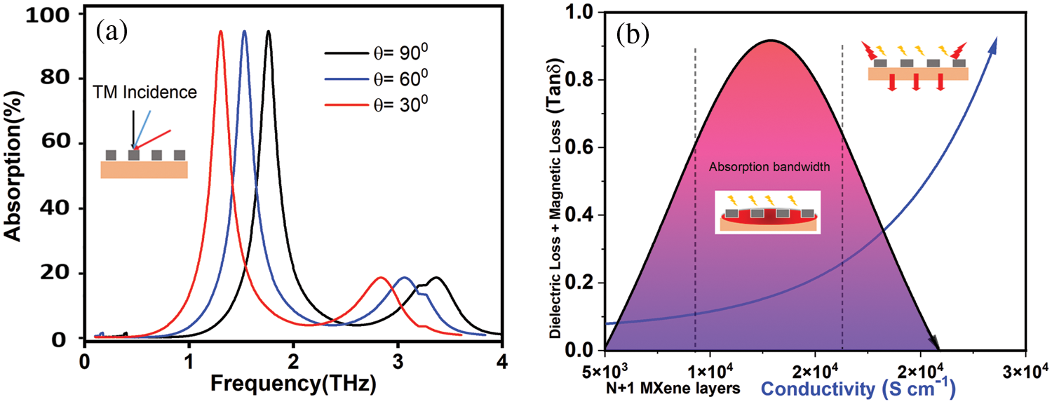
Figure 5: (a) Spectra of absorption resonance with change in the incidence angle of THz source wave. Resonance tuning of 0.6 THz bandwidth is realized when the incidence angle is changed from θ = 90° to θ = 30° while maintaining the peak absorption value, (b) conductivity versus impedance matching, increase in MXene layer raises the conductivity at the absorption resonance with better impedance matching, although a large increase in the conductivity can produce high losses and miss matching at the resonance frequency (1.8 THz) which can result in shifting of resonance position to other frequencies. Hence to retain a higher absorption value at the resonance frequency, a balanced is required between the conductivity, dielectric and magnetic loss
Further decreasing the incidence angle to θ = 30° the absorption resonance to 1.2 THz center frequency. Fig. 5a also depicts the stability of resonance absorption when there is a change in the source incidence angle. The potential use of angle-independent absorption in shielding is particularly important. As the incidence angle increases from 30° to 90° degrees, the strength of the absorption remains relatively constant at the resonant frequencies. It should be noted that for TM polarization, when the source incidence angle is varied, the magnetic x-y component of the wave remains unchanged and does not affect the absorption resonance intensity but can significantly provide resonance tuning. To design EM absorption materials properly, good EM energy attenuation and great impedance matching are often taken into account. However high electrical conductivity resulting in high impedance mismatching is needed to improve the EMI shielding performance of the material. Meanwhile, a key factor in the loss of EM energy is the interaction between magnetic loss and dielectric characteristics. In light of these considerations, the secret to designing high-performance EM wave absorption and shielding materials is to balance the dielectric characteristics, permeability, and electrical conductivity. As shown in Fig. 5b, the link between the conductor/magnet component ratio and the EM wave absorption with shielding properties is provided in a phase diagram based on our findings. This stable property of resonance in metamaterial is very useful in THz shielding and biosensing, where even a small change in the efficiency of absorption can make device prototyping impossible.
In Fig. 6, the illustrations of confined plasmonic field and surface plasmon resonance propagation are given. The plots reveal the resonance behavior of the surface plasmon fields when the top surface of the metamaterial is illuminated by the incident source. Fig. 6a shows the plasmonic excitation and the coupling of the plasmonic field when the thickness is hm = 30 nm. The plasmons originate from the sharp corners of the MXene square-shaped resonators and produce a dipole-like pattern. The highly localized field confinement (hm = 50 nm) can be seen in Fig. 6b, where the near-field mutual coupling of the nearest array elements results in higher absorption. The enhancement of the field can be observed at the center and corners of the MXene resonator. The top MXene material spatial placement arises in plasmon resonance, and the plasmon near-field coupling is the advantage of this ultrahigh absorption at the terahertz region. Furthermore, interlayer coupling of plasmons also plays a role in the significant amount of light absorption because of the forward and backward waves in the cavity region between the layers. The surface current plots in Figs. 6c and 6d illustrate the corresponding current distribution related to the MXene thickness. It can be observed, when the layer thickness is increased, the polarization of the field also changes from horizontal to vertical polarization. The absorption enhancement is also analyzed using a cross-sectional view when the MXene thickness is raised. The Figs. 6e–6g illustrate the absorption field strength from 30 to 50 nm. In comparison, the field strength at 30 nm has less intensity due to losses and also low absorption. Although a high field intensity of absorption is achieved when the thickness is raised to 50 nm. The higher field intensity of absorption reveals that the metasurface structure is better impedance matched where it can absorb 95% of incident source energy, providing higher EMI shielding effectiveness. Additionally, magnetic resonance is caused by the strong interactions between the magnetic field of the incoming THz source and the antiparallel electric currents created in the top MXene layer and the lower MXene layer. The localized field confinement provides enhanced absorption at the resonance frequency, which in turn improves the shielding performance. The achieved shielding in this study is far better than recent investigations [14,16,17,24,25].
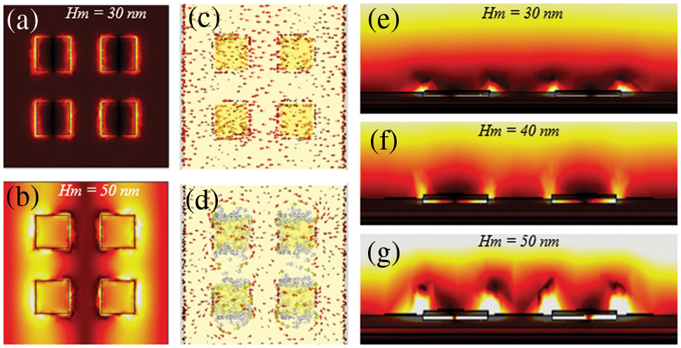
Figure 6: Visualization of plasmonic field confinement and surface plasmon propagation in MXene metamaterial unit cell (a) origination of surface plasmon fields at the corners of metasurface unit cell at 30 nm, (b) the plasmonic field enhancement due to interlayer coupling and the effective coupling between the adjacent unit cells of the metasurface when the thickness is 50 nm. (c and d) The corresponding surface current distribution on the resonators structure with increasing thickness. (e and g) Cross-sectional view of the metasurface absorption intensity relative to increasing thickness
In conclusion, the emerging 2D nanomaterial, MXene-based metamaterial is being investigated in the realm of terahertz plasmonics. The Drude-Lorentz model is used in this study to calculate the dielectric parameters in the terahertz range. The proposed metamaterial obtained high absorption in the terahertz region with a wide bandwidth. The absorption of 95% is realized under the normal incidence of the terahertz wave. This higher absorption results from the individual nearfield coupling of array elements, which adds up by providing highly localized field enhancement at the center of each MXene resonator. The tunability of performance is demonstrated with the thickness and incidence angle changes providing a shift in the resonance frequency at the terahertz region. Furthermore, the shielding performance is highly dependent on absorption. The outcomes of this study could benefit applications involving stealth and sensing in the terahertz region.
Acknowledgement: This research is a joint venture of research collaboration between Al-Ain university, UAE, and Durham University, UK, and funded by Abu Dhabi Award for Research Excellence (AARE19-245). We also acknowledge the efforts and contribution towards this research by Universiti Teknologi PETRONAS.
Funding Statement: This research is funded by Abu Dhabi Award for Research Excellence (AARE19-245).
Conflicts of Interest: The authors declare that they have no conflicts of interest to report regarding the present study.
References
1. L. Liang, G. Han, Y. Li, B. Zhao, B. Zhou et al., “Promising Ti3C2Tx MXene/Ni chain hybrid with excellent electromagnetic wave absorption and shielding capacity,” ACS Applied Materials and Interfaces, vol. 11, no. 28, pp. 25399–25409, 2019. [Google Scholar] [PubMed]
2. X. Zhang, Q. Xu, L. Xia, Y. Li, J. Gu et al., “Terahertz surface plasmonic waves: A review,” Advanced Photonics, vol. 2, no. 1, pp. 1–19, 2020. [Google Scholar]
3. K. Zeranska-Chudek, A. Lapinska, A. Siemion, A. M. Jastrzębska and M. Zdrojek, “Terahertz time domain spectroscopy of graphene and MXene polymer composites,” Journal of Applied Polymer Science, vol. 138, no. 10, pp. 1–7, 2021. [Google Scholar]
4. Z. Jakšić, M. Obradov, D. Tanasković, O. Jakšić and D. Vasiljević Radović, “Electromagnetic simulation of MXene-based plasmonic metamaterials with enhanced optical absorption,” Optical and Quantum Electronics, vol. 52, no. 2, pp. 1–10, 2020. [Google Scholar]
5. Y. Zhang, H. Dong, N. Mou, L. Chen, R. Li et al., “High-performance broadband electromagnetic interference shielding optical window based on a metamaterial absorber,” Optics Express, vol. 28, no. 18, pp. 26836, 2020. [Google Scholar] [PubMed]
6. J. Jeon, Y. Yang, H. Choi, J. H. Park, B. H. Lee et al., “MXenes for future nanophotonic device applications,” Nanophotonics, vol. 9, no. 7, pp. 1831–1853, 2020. [Google Scholar]
7. Z. Jiang, S. Zhao, L. Chen and Y. Liu, “Freestanding ‘core-shell’ AgNWs/metallic hybrid mesh electrodes for a highly efficient transparent electromagnetic interference shielding film,” Optics Express, vol. 29, no. 12, pp. 18760, 2021. [Google Scholar] [PubMed]
8. L. Li, M. Shi, X. Liu, X. Jin, Y. Cao et al., “Ultrathin titanium carbide (MXene) films for high-temperature thermal camouflage,” Advanced Functional Materials, vol. 31, no. 35, pp. 1–10, 2021. [Google Scholar]
9. R. Mitsuhashi, K. Murate, S. Niijima, T. Horiuchi and K. Kawase, “Terahertz tag identifiable through shielding materials using machine learning,” Optics Express, vol. 28, no. 3, pp. 3517, 2020. [Google Scholar] [PubMed]
10. A. J. A. Al-Gburi, I. M. Ibrahim, K. S. Ahmad, Z. Zakaria, M. Y. Zeain et al., “A miniaturised UWB FSS with stop-band characteristics for EM shielding applications,” Przeglad Elektrotechniczny, vol. 97, no. 8, pp. 142–145, 2021. [Google Scholar]
11. L. Yao, Y. Liang, K. Wen, Y. Xu, J. Liu et al., “Demonstration of tunable shielding effectiveness in GHz and THz bands for flexible graphene/ion gel/graphene film,” Applied Sciences, vol. 11, no. 11, pp. 5133, 2021. [Google Scholar]
12. M. B. Hossain, M. R. I. Faruque, M. T. Islam, M. Singh and M. Jusoh, “Triple band microwave metamaterial absorber based on double E-shaped symmetric split ring resonators for EMI shielding and stealth applications,” Journal of Materials Research and Technology, vol. 18, no. 1, pp. 1653–1668, 2022. [Google Scholar]
13. Y. Kou, K. Jin and X. Zheng, “Numerical simulation on the shielding efficiency of magnetic shielding enclosures in the ITER applications,” Computers, Materials and Continua, vol. 22, no. 2, pp. 129–146, 2011. [Google Scholar]
14. Y. Lu, S. Zhang, M. He, L. Wei, Y. Chen et al., “3D cross-linked graphene or/and MXene based nanomaterials for electromagnetic wave absorbing and shielding,” Carbon, vol. 178, no. 7, pp. 413–435, 2021. [Google Scholar]
15. H. Chu, H. Zhang, Y. Zhang, R. Peng, M. Wang et al., “Invisible surfaces enabled by the coalescence of anti-reflection and wavefront controllability in ultrathin metasurfaces,” Nature Communications, vol. 12, no. 1, pp. 1–7, 2021. [Google Scholar]
16. K. Chaudhuri, M. Alhabeb, Z. Wang, V. M. Shalaev, Y. Gogotsi et al., “Highly broadband absorber using plasmonic titanium carbide (MXene),” ACS Photonics, vol. 5, no. 3, pp. 1115–1122, 2018. [Google Scholar]
17. H. Ren, S. Wang, X. Zhang, Y. Liu, L. Kong et al., “Broadband electromagnetic absorption of Ti3C2Tx MXene/WS2 composite via constructing two-dimensional heterostructure,” Journal of the American Ceramic Society, vol. 104, no. 11, pp. 5537–5546, 2021. [Google Scholar]
18. V. Shukla, “Review of electromagnetic interference shielding materials fabricated by iron ingredients,” Nanoscale Advances, vol. 1, no. 5, pp. 1640–1671, 2019. [Google Scholar] [PubMed]
19. O. Salim, K. A. Mahmoud, K. K. Pant and R. K. Joshi, “Introduction to MXenes: Synthesis and characteristics,” Materials Today Chemistry, vol. 14, pp. 100191, 2019. [Google Scholar]
20. D. B. Velusamy, J. K. El-Demellawi, A. M. El-Zohry, A. Giugni, S. Lopatin et al., “MXenes for plasmonic photodetection,” Advanced Materials, vol. 31, no. 32, pp. 1–10, 2019. [Google Scholar]
21. Z. Wang, K. Chaudhuri, M. Alhabeb, X. Meng, S. I. Azzam et al., “MXenes for plasmonic and metamaterial devices,” in Proc. Conf. on Laser and Electro-Optics, California, CL, USA, pp. 6–7, 2018. [Google Scholar]
22. Y. I. Jhon, M. Seo and Y. M. Jhon, “First-principles study of a MXene terahertz detector,” Nanoscale, vol. 10, no. 1, pp. 69–75, 2018. [Google Scholar]
23. Y. Zhu, J. Liu, T. Guo, J. J. Wang, X. Tang et al., “Multifunctional Ti3C2Tx MXene composite hydrogels with strain sensitivity toward absorption-dominated electromagnetic-interference shielding,” ACS Nano, vol. 15, no. 1, pp. 1465–1474, 2021. [Google Scholar] [PubMed]
24. G. Choi, F. Shahzad, Y. M. Bahk, Y. M. Jhon, H. Park et al., “Enhanced terahertz shielding of MXenes with nano-metamaterials,” Advanced Optical Materials, vol. 6, no. 5, pp. 1–6, 2018. [Google Scholar]
25. W. Shui, J. Li, H. Wang, Y. Xing, Y. Li et al., “Ti3C2Tx MXene sponge composite as broadband terahertz absorber,” Advanced Optical Materials, vol. 8, no. 21, pp. 1–8, 2020. [Google Scholar]
26. W. Ma, H. Chen, S. Hou, Z. Huang, Y. Huang et al., “Compressible highly stable 3D porous MXene/GO foam with a tunable high-performance stealth property in the terahertz band,” ACS Applied Materials and Interfaces, vol. 11, no. 28, pp. 25369–25377, 2019. [Google Scholar] [PubMed]
27. W. Cui, L. Li, W. Xue, H. Xu, Z. He et al., “Enhanced absorption for MXene/Au-based metamaterials,” Results in Physics, vol. 23, pp. 104072, 2021. [Google Scholar]
28. Y. Liu, X. Li, T. Yang, J. Liu, B. Liu et al., “Flexible broadband terahertz modulation based on strain-sensitive MXene material,” Frontiers in Physics, vol. 9, no. May, pp. 1–7, 2021. [Google Scholar]
29. G. Chakraborty, S. Chattopadhyay, C. K. Sarkar and C. Pramanik, “Tunneling current at the interface of silicon and silicon dioxide partly embedded with silicon nanocrystals in metal oxide semiconductor structures,” Journal of Applied Physics, vol. 101, no. 2, pp. 024315, 2007. [Google Scholar]
30. Y. F. Li and Z. P. Liu, “Smallest stable Si/SiO interface that suppresses quantum tunneling from lachine-learning based global search,” Physical Review Letters, vol. 128, no. 22, pp. 226102, 2022. [Google Scholar] [PubMed]
31. L. Wu, Q. You, Y. Shan, S. Gan, Y. Zhao et al., “Few-layer Ti3C2Tx MXene: A promising surface plasmon resonance biosensing material to enhance the sensitivity,” Sensors and Actuators, B: Chemical, vol. 277, no. June, pp. 210–215, 2018. [Google Scholar]
32. Q. Zou, W. Guo, L. Zhang, L. Yang, Z. Zhao et al., “MXene-based ultra-thin film for terahertz radiation shielding,” Nanotechnology, vol. 31, no. 50, pp. 505710, 2020. [Google Scholar] [PubMed]
33. U. Hwang, J. Kim, M. Seol, B. Lee, I. K. Park et al., “Quantitative interpretation of electromagnetic interference shielding efficiency: Is it really a wave absorber or a reflector?,” ACS Omega, vol. 7, no. 5, pp. 4135–4139, 2022. [Google Scholar] [PubMed]
Cite This Article
 Copyright © 2023 The Author(s). Published by Tech Science Press.
This work is licensed under a Creative Commons Attribution 4.0 International License , which permits unrestricted use, distribution, and reproduction in any medium, provided the original work is properly cited.
 Downloads
 Citation Tools