
 Submit a Paper
 Propose a Special lssue
 Open Access
ARTICLE

Design and Analysis of Graphene Based Tunnel Field Effect Transistor with Various Ambipolar Reducing Techniques
1 Department of Electronics and Communication Engineering, G L Bajaj Institute of Technology and Manegment, Gretear Noida, India
2 Department of Electronics and Communication Engineering, Chandigarh Unievrsity, Mohali, Punjab, India
3 Department of Electronics and Communication Engineering, NITTTR, Chandigarh, India
4 University Center of Research & Development, Chandigarh University, Mohali, 121102, India
5 Department of Computer Science, College of Computer and Information Sciences, Majmaah University, Al-Majmaah, 11952, Saudi Arabia
6 Department of Mathematics, College of Science Al-Zulfi, Majmaah University, 11952, Al-Majmaah, Saudi Arabia
7 Electrical Engineering Department, Faculty of Engineering & Technology, Future University in Egypt, New Cairo, 11835, Egypt
* Corresponding Author: Mohd Anul Haq. Email:
Computers, Materials & Continua 2023, 76(1), 1309-1320. https://doi.org/10.32604/cmc.2023.033828
Received 29 June 2022; Accepted 08 December 2022; Issue published 08 June 2023
 View Full Text
 Download PDF
Abstract
The fundamental advantages of carbon-based graphene material, such as its high tunnelling probability, symmetric band structure (linear dependence of the energy band on the wave direction), low effective mass, and characteristics of its 2D atomic layers, are the main focus of this research work. The impact of channel thickness, gate under-lap, asymmetric source/drain doping method, workfunction of gate contact, and High-K material on Graphene-based Tunnel Field Effect Transistor (TFET) is analyzed with 20 nm technology. Physical modelling and electrical characteristic performance have been simulated using the Atlas device simulator of SILVACO TCAD with user-defined material syntax for the newly included graphene material in comparison to silicon carbide (SiC). The simulation results in significant suppression of ambipolar current to voltage characteristics of TFET and modelled device exhibits a significant improvement in subthreshold swing (0.0159 V/decade), the ratio of Ion/Ioff (1000), and threshold voltage (−0.2 V with highly doped p-type source and 0.2 V with highly doped n-type drain) with power supply of 0.5 V, which make it useful for low power digital applications.Keywords
A carbon based substance called graphene has exceptional carrier mobility (125,000 Cm2/V-Sec), high tunnelling probability, and high Fermi velocity, among other distinctive electronic transport features [1,2]. Excellent thermal conductivity, great mechanical strength, thinness, and flexibility are further benefits of these characteristics. These qualities make graphene a superb option for cutting-edge electrical applications in the future [3].
A current trending device is modelled for low power a Very Large Scale Integration (VLSI) application, namely a Tunnel Field Effect Transistor (TFET), using the extraordinarily high tunnelling probability and carrier mobility of graphene material. In comparison to Silicon based standard Metal Oxide Field Effect Transistor (MOSFET), TFET has a better transport mechanism of carriers and is an improved contender for low power dissipation and high noise margin digital switch applications with low value sub threshold slope [2,4].
2 Graphene Material: Basic Structure, Electronic Properties and Electronic Transport
A mechanical exfoliation process was initially used to extract graphene, a single atomic layer of graphite, from graphite [3]. The only place it has in the periodic table is beneath Silicon. Fig. 1 was created with the aid of the Ninithi Computer Aided Design (CAD) tool by the Lanka Software Foundation, which can visualise the molecular geometries of graphene [2–5]. Carbon allotropes such as graphite (3D number of graphene sheets is shown in Fig. 1a), carbon nanotubes (1D rolled up graphene cylinder is shown in Fig. 1b), and fullerenes (0D molecules wrapped up graphene with the introduction of pentagons is shown in Fig. 1c).
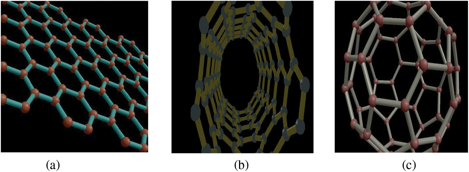
Figure 1: Carbon allotropes (a) Graphene, (b) Carbon nanotubes and (c) Fullerene
Graphene consists of two carbon atoms per unit cells A & B, which are arranged in the form of a diamond honeycomb lattice as illustrated in Fig. 2a. A constant lattice achieved for this material is of 1.42 Å [3–7]. High carrier mobility in graphene is caused by the valence electrons of carbon atoms being sp2 hybridised with the remaining pz carbon orbital to generate an extended π-electron. Each carbon atom has a π bond shared with its closest neighbours, which causes the valence band to be formed by the π-states and the conduction band by the π*-states. These two bands come into contact at six points, which are known as Dirac or neutrality points and produce a linear relationship between the energy band gap and wave vector. Symmetry allows these six points to be reduced by a pair of independent points K and K’ as shown in Fig. 2b. Fig. 2c illustrates a linear relationship between the energy band and the wave vector.
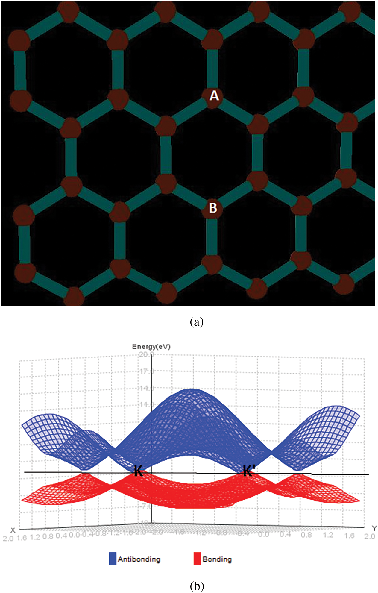

Figure 2: Graphene material; (a) Hexagonal honeycomb lattice of Graphene with two atoms (A and B) in per unit cell, (b)Tight binding band structure of Graphene bands with K and K′ as π bonding and π*antibonding point (c) Band structure near Dirac point showing the linear dispersion relation using VNL-ATK tool [9,10]
where νF and k are the Fermi velocity and the wave vector respectively. The symbol ħ denotes the reduced Planck constant and equals h/2π [3,6].
In contrast to other typical semiconductors like Si, Ge, and GaAs, where the mobility of carriers is asymmetric with a parabolic band gap and exhibits a potential of mobility; 3000 125,000 cm3/V.sec [6–8], the symmetry of π-states and π*-states around the Dirac points suggests that the electron and the hole should have equal mobility. Additionally, due to significantly faster electron mobility than equivalent silicon transistors, graphene has good potential for higher clock rates [3–8].
3 Graphene TFET: Structure and Operation
A p-i-n gated diode with a double gate (fgate & cgate) regulated mechanism is the basis of the graphene TFET construction. As shown in Fig. 3, it consists of an intrinsic channel region (the horizontal length of 20 nm and doped with 1 × 10¹⁷ atoms/cm3 also with thickness 2 nm) in between two layers of dielectric material with a width of 1 nm, a p+ source and an n+drain, each with a horizontal length of 5 nm and doped with 3.18 × 10²⁰ atoms/cm3. After Graphene ambipolar properties were discovered, Graphene TFET was made feasible [2,11–14].
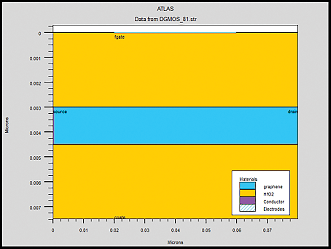
Figure 3: Schematic structure of Graphene TFET
Typical metals are used for making electrode contacts with different work functions for gate contact by definition in Atlas device simulation [15–17]. These contacts are selected owing to their ability to control the contact resistance, which gives novelty in the result. Controlling contact resistance enhances device performance overall, particularly for ballistic transport mechanisms with high mobility made of graphene. The contact between graphene and metal is therefore an ohmic one [15,16], but occasionally the low density of state (DOS) in graphene may prevent the injection of current. Additionally, the Graphene TFET’s gate dielectric should have a high dielectric constant and be extremely thin and homogeneous. In addition, there should be very little DOS at the interface. HfO2 and Al2O3 are two frequently utilised high-materials that can be formed utilising the atomic layer deposition approach [12–14,18].
4 Device Modelling and Simulation
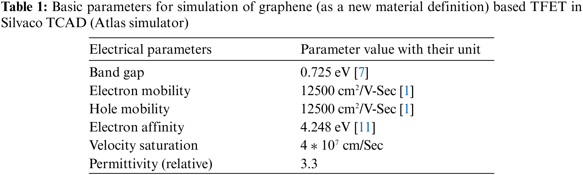
The Silvaco TCAD programme is used with user-defined syntax for new materials with their parameter as indicated in Table 1 to model the electrical properties of Graphene TFETs. Permittivity is mapped following the material characteristics of graphene to model graphene inside the TCAD materials environment with parameters of band gap, holes, and electron mobility [17].
By applying the Wentzel-Kramers-Brillouin (WKB) approximation and imposing the tunnel barrier as a triangularly shaped potential barrier, as shown in Fig. 4, it is possible to get the formula for band-to-band tunnelling current in TFETs. The band-to-band tunnelling transmission (Tt) is given by [19–26] using the WKB approximation;

Figure 4: Current transfer characteristic of Graphene TFET
where,
Here, PE is the potential energy, and E is the energy of the incoming electron, m is the electron’s mass. Now average PE is related to the band gap as
From Eqs. (2) and (4), the band-to-band tunnelling transmission can be modified as;
By considering,
On solving, Tt is simplified as;
Eq. (7) is a general expression for band-to-band tunnelling transmission. Band tunnelling strongly depends upon Eg and the paper also shows that Graphene material has the ability to the tunable band gap. Therefore, the Eg is adjusted in such a manner that the Graphene TFET dissipate less power as compared to conventional FET [27–29].
5 Extraction of Performance Parameters for Graphene TFET
Firstly, the sub-threshold swing (SS) is calculated and I-V characteristics of Graphene TFET are observed, which shows ambipolar characteristics and thereafter multiple techniques are utilized, which reduce the ambipolar current characteristic of graphene-based tunnel field effect transistor.
5.1 Subthreshold Swing in TFETs
Starting on Sze’s expression [20] for the tunnelling current (IDS) across a reverse biased PN junction, one can obtain an expression for the subthreshold swing of a band-to-band tunnelling device.
where, Veff is the bias voltage of the tunnel junction and
and
Subsequently, the subthreshold swing is calculated as;
By solving the expression of subthreshold swing (Eq. (11)) based on Eqs. (8)–(10), the simplified expression can be written as;
According to Eq. (12), the subthreshold swing varies concerning the bias voltage of the tunnel junction, whereas in the case of conventional FET, it was approximately constant as ln10 [18,21,26,27].
5.2 Transfer Characteristics at Different Technology Nodes
With the use of a physical and mathematical model called NEWTON and a maximum of four traps, a Graphene TFET is simulated using the ATLAS simulator for band to band tunnelling. The current is first calculated at each step bias point and then solved over the swept bias variable at each stepped point [22] in order to build the IDS vs. VGS characteristics curve. For instance, for VDS = 0.5 V, solutions are obtained for each VGS value, and the results of these solutions are logged in the.log file (solution file). The gate voltage (VGS) is swept from −0.6 to 0.6 V with a step size of 0.1 V, while the drain voltage (VDS) is set at 0.5 V and the Tony Plot is then used to overlay two IDS-VGS curves, as seen in Fig. 4.
The device obtains current values for both negative and positive VGS, according to the plot of logarithmic current values (log10IDS) as a function of VGS for Graphene TFET. This curve exhibits two-direction conduction (ambipolar characteristics), and as seen in Fig. 4, the curve also exhibits a minimum conduction point at VGS = 0 V.
5.2.1 Transfer Characteristics as a Function of Metal’s Work function
To understand the suitability of the metal as an electrode, the proposed Graphene TFET is examined at various work functions of the metal electrodes. Fig. 5 shows the transfer characteristic of Graphene TFET for various work functions ranging from 4.21 to 4.61 eV.

Figure 5: Characteristic curves of IDS vs. VGS as a function of metal’s work functions
As can be seen from Fig. 5, Imin is equal to zero when the work function is 4.41 eV, and it is greater when the work function is 4.61 or 4.21 eV when the gate to source voltage is grounded. It is shown that the material with a work function of 4.41 eV is ideal for use in low-power VLSI’s graphene TFET. The ‘off’ current of the graphene TFET at VGS = 0 dramatically increases at work functions other than 4.41 eV (Imin > 0), resulting in a significant leakage current. As long as a specific metal is used for the electrode terminal, the graphene TFET can be employed for low power applications.
5.2.2 Transfer Characteristics Concerning Gate Underlap
Many researchers have proposed numerous methods based on gate underlap & asymmetric doping of the source/drain region to lessen the ambipolarity of semiconductors. The gate underlaps at each end of the channel have a significant impact on how current behaves in the device. Graphene TFET’s IDS- VGS characteristic with respect to various gate underlap values is depicted in Fig. 6; the various gate underlap values are 10, 20, and 30 nm.

Figure 6: Current transfer characteristics of Grapheme TFET as a function of gate underlap
This study shows that by using gate underlap, the primary drawback of TFET, ambipolarity, may be significantly reduced. When gate underlap is applied at the source side, the n-type conduction is greatly reduced, while the p-type conduction is unaffected. Raising the potential barrier at the negative gate to source potential has the effect of decreasing the overall tunnelling current.
5.2.3 Transfer Characteristics Concerning Asymmetric Doping
The energy band structure of the Graphene TFET is also altered by asymmetric doping of the source/drain area. It results in a noticeable decrease in the overall tunnelling current and raises the potential barrier when the device is in its off state, which is represented by a negative bias at the gate to the source terminal.
Graphene TFET combined current transfer characteristics for various asymmetric doping levels, including 1010, 1012, and 1014 atom/cm3, are plotted in Fig. 7. The investigation shows that TFET has a downside (i.e., ambipolarity can be reduced by using asymmetric doping level).

Figure 7: Current transfer characteristic of Graphene TFET concerning asymmetric doping
5.2.4 Transfer Characteristics at Different Channel Thickness
A crucial factor that can impact the band gap of this material, which is not feasible for conventional semiconductor materials (Si & Ge), is the thickness of graphene, or tGraphene (tPGC). Since the current of a grapheme TFET depends on the total charge that has been filled in the subband [15,21–23], the tGraphene will also be a factor (tPGC). Fig. 8 displays the results of a simulation of the current transfer characteristics of Graphene TFETs for tGraphene at 1, 1.6, and 2 nm. The findings show that altering the channel thickness can effectively lessen the ambipolarity of graphene TFETs.

Figure 8: Current transfer characteristic of Graphene TFET with varying film thickness
5.2.5 Transfer Characteristics at Different Dielectric Materials
The strength of the dielectric material is a further variable that can have an impact on the current characteristics of graphene TFETs. In this analysis, various dielectric materials including HfO2, SiO2, and Si3N4 are taken into account. The results are shown in Fig. 9. For all dielectric materials with minimum value, the total current is identical at VGS = 0 V, but when the gate to source voltage varies, the current also varies and exhibits ambipolar behaviour.

Figure 9: Current transfer characteristic of Graphene TFET to different dielectrics
The Graphene TFET with HfO2 shows the best current voltage characteristic and is thus found as the most suitable material while designing Graphene TFET. On changing dielectric from SiO2 to HfO2 (ε ~ 25), the threshold voltage and subthreshold swing both drop at the half, and the current augments by several orders of magnitude (1 × 10⁻⁶ A to 1 × 10⁻⁵ A). The variation of the permittivity has a severe influence on all the characteristic parameters, especially when changing from a relatively low permittivity material; SiO2 (3.9) to high-k dielectric HfO2 [26].
This study concluded that factors such as gate underlap, asymmetric doping, channel thickness, the work function of the gate electrode, and the properties of the dielectric depend on the current conduction in TFETs. Due to the unique electrical characteristics of graphene material, the aforementioned result is more significant when compared to conventional semiconductor materials in terms of all aspects, and the device has demonstrated the advantage, particularly with reducing ambipolar current characteristic of Graphene TFET, which is useful for digital design. The advantage of Graphene Tunnel FET is also discussed in terms of minimum IDS at VGS = 0 V (10−8 A), maximum IDS at VGS = VDD V (10−5 A), and the ratio of Ion/Ioff (1000). Additionally, results show that Graphene TFET offers high switching performance applications due to its steeper sub-threshold swing compared to conventional semiconductor materials. When compared to conventional MOSFETs, the device’s low value, temperature independence, and high on/off ratio provide nearly optimal switching applications.
Funding Statement: Mohd Anul Haq would like to thank Deanship of Scientific Research at Majmaah University for supporting this work under Project No. R-2022-###.
Conflicts of Interest: The authors declare that they have no conflicts of interest to report regarding the present study.
References
1. S. Vaziri, “Fabrication and characterization of graphene field effect transistors,” M.S. thesis, School of Information and Communication Technology (ICT2011. [Google Scholar]
2. F. Schweirz, “Graphene transistors,” Nature Nanotechnology, vol. 5, no. 7, pp. 487–496, 2010. [Google Scholar] [PubMed]
3. A. K. Geim, “Graphene: Status and prospects,” Science 324, vol. 5934, pp. 1530–1534, 2009. [Google Scholar]
4. M. R. Moslemi, M. H. Sheikhi, K. Saghafi and M. K. Moravvej-Farshi, “Electronic properties of a dual-gated GNR-FET under uniaxial tensile strain,” Microelectronics Reliability, vol. 52, no. 11, pp. 2579–2584, 2012. [Google Scholar]
5. T. O. Wehling, K. S. Novoselov, S. V. Morozov, E. E. Vdovin, M. I. Katsnelson et al., “Molecular doping of grapheme,” Nano Letters, vol. 8, no. 1, pp. 173–177, 2008. [Google Scholar] [PubMed]
6. P. Avouris, “Graphene: Electronic and photonic properties and devices,” Nano Letters, vol. 10, no. 11, pp. 4285–4294, 2010. [Google Scholar] [PubMed]
7. S. Negi, P. Mittal and B. Kumar, “Impact of different layers on performance of OLED,” Microsystem Technologies, vol. 24, no. 12, pp. 4981–4989, 2018. [Google Scholar]
8. J. Kedzierski, P. L. Hsu, P. Healey, P. W. Wyatt, C. L. Keast et al., “Epitaxial graphene transistors on SiC substrates,” IEEE Transactions on Electron Devices, vol. 55, no. 8, pp. 2078–2085, 2008. [Google Scholar]
9. B. Guo, L. Fang, B. Zhang and J. R. Gong, “Graphene doping: A review,” Insciences Journal, vol. 1, no. 2, pp. 80–89, 2010. [Google Scholar]
10. V. Narendar, S. K. Gupta and S. Saxena, “First principle study of doped graphene for FET applications,” Silicon, vol. 11, no. 1, pp. 277–286, 2019. [Google Scholar]
11. H. Zhou, Y. Hao and M. Zhang, “Performance optimization of MOS-like Carbon Nanotubes-FETs with realistic source/drain contacts based on electronic doping,” Journal of Semiconductor, vol. 31, no. 12, pp. 124005-2–124005-6, 2010. [Google Scholar]
12. K. Boucart and A. M. Ionescu, “Double-gate tunnel FET with high-κ gate dielectric,” IEEE Transactions on Electron Devices, vol. 54, no. 7, pp. 1725–1733, 2007. [Google Scholar]
13. N. Paras and S. S. Chauhan, “A novel vertical tunneling based Ge-source TFET with enhanced DC and RF characteristics for prospect low power applications,” Microelectronic Engineering, vol. 217, no. 4, pp. 111103, 2019. [Google Scholar]
14. A. M. M. Hammam, M. E. Schmidt, M. Muruganathan, S. Suzuki and H. Mizuta, “Sub-10 nm graphene nano-ribbon tunnel field-effect transistor,” Carbon, vol. 126, pp. 588–593, 2018. [Google Scholar]
15. E. J. H. Lee, K. Balasubramanian, R. T. Weitz, M. Burghard and K. Kern, “Contact and edge effects in graphene devices,” Nature Nanotechnology, vol. 3, no. 8, pp. 486–490, 2008. [Google Scholar] [PubMed]
16. J. A. Robinson, M. LaBella, M. Zhu, M. Hollander, R. Kasarda et al., “Contacting graphene,” Applied Physics Letter, vol. 98, no. 5, pp. 053103, 2011. [Google Scholar]
17. Manual, ATLAS User’S, Device simulation software, Santa Clara: SILVACO international, 2012. [Google Scholar]
18. B. R. Raad, K. Nigam, D. Sharma and P. N. Kondekar, “Performance investigation of bandgap, gate material work function and gate dielectric engineered TFET with device reliability improvement,” Superlattices and Microstructures, vol. 94, no. 4, pp. 138–146, 2016. [Google Scholar]
19. J. D. Plummer, Silicon VLSI technology: Fundamentals, Practice and Modeling, India: Pearson Education, 2009. [Google Scholar]
20. S. M. Sze, Y. Li and K. K. Ng, Physics of Semiconductor Devices, Hoboken, New Jersey: John Wiley & Sons, 2021. [Google Scholar]
21. F. Xia, D. B. Farmer, Y. Lin and P. Avouris, “Graphene field-effect transistors with high on/off current ratio and large transport band gap at room temperature,” Nano Letters, vol. 10, no. 2, pp. 715–718, 2010. [Google Scholar] [PubMed]
22. K. Shimizu and T. Hiramoto, “Mobility enhancement in uniaxially strained (110) oriented ultra-thin body single-and double-gate MOSFETs with SOI thickness of less than 4 nm,” in 2007 IEEE Int. Electron Devices Meeting, Washington DC, pp. 715–718, 2007. [Google Scholar]
23. H. Wang, A. Hsu, J. Kong, D. A. Antoniadis and T. Palacios, “Compact virtual-source current-voltage model for top-and back-gated graphene field-effect transistors,” IEEE Transactions on Electron Devices, vol. 58, no. 5, pp. 1523–1533, 2011. [Google Scholar]
24. H. Y. Chang, S. Chopra, B. Adams, J. Li, S. Sharma et al., “Improved subthreshold characteristics in tunnel field-effect transistors using shallow junction technologies,” Solid-State Electronics, vol. 80, pp. 59–62, 2013. [Google Scholar]
25. J. W. Lee and W. Y. Choi, “Design guideline of tunnel field-effect transistors (TFETs) considering negative differential transconductance (NDT),” Solid-State Electronics, vol. 163, no. 12, pp. 107659, 2020. [Google Scholar]
26. S. Vidhyadharan, S. S. Dan, S. V. Abhay, R. Yadav and S. Hariprasad, “Novel gate-overlap tunnel FET based innovative ultra-low-power ternary flash ADC,” Integration, vol. 73, no. 1, pp. 101–113, 2020. [Google Scholar]
27. P. K. Mishra, A. Rai and M. Rai, “Dynamic threshold MOSFET for low power VLSI circuit design,” International Journal of Electronics and Technology, vol. 7, pp. 932–935, 2018. [Google Scholar]
28. P. G. Der Agopian, J. A. Martino, A. Vandooren, R. Rooyackers, E. Simoen et al., “Study of line-TFET analog performance comparing with other TFET and MOSFET architectures,” Solid-State Electronics, vol. 128, no. 12, pp. 43–47, 2017. [Google Scholar]
29. M. A. Eshkalak and M. K. Anvarifard, “A novel graphene nanoribbon FET with an extra peak electric field (EFP-GNRFET) for enhancing the electrical performances,” Physics Letters A, vol. 381, no. 16, pp. 1379–1385, 2017. [Google Scholar]
Cite This Article
 Copyright © 2023 The Author(s). Published by Tech Science Press.
This work is licensed under a Creative Commons Attribution 4.0 International License , which permits unrestricted use, distribution, and reproduction in any medium, provided the original work is properly cited.
 Downloads
 Citation Tools