
 Submit a Paper
 Propose a Special lssue
 Open Access
ARTICLE

Royal Crown Shaped Polarization Insensitive Perfect Metamaterial Absorber for C-, X-, and Ku-Band Applications
1 Space Science Centre (ANGKASA), Institute of Climate Change (IPI), Universiti Kebangsaan Malaysia, UKM, Bangi, 43600, Selangor D. E., Malaysia
2 Department of Electrical, Electronic & Systems Engineering, Faculty of Engineering & Built Environment, Universiti Kebangsaan Malaysia, UKM, Bangi, 43600, Selangor D. E., Malaysia
* Corresponding Author: Mohammad Rashed Iqbal Faruque. Email:
Computers, Materials & Continua 2023, 76(1), 455-469. https://doi.org/10.32604/cmc.2023.036655
Received 08 October 2022; Accepted 15 March 2023; Issue published 08 June 2023
 View Full Text
 Download PDF
Abstract
This study proposed a new royal crown-shaped polarisation insensitive double negative triple band microwave range electromagnetic metamaterial absorber (MA). The primary purpose of this study is to utilise the exotic characteristics of this perfect metamaterial absorber (PMA) for microwave wireless communications. The fundamental unit cell of the proposed MA consists of two pentagonal-shaped resonators and two inverse C-shaped metallic components surrounded by a split ring resonator (SRR). The bottom thin copper deposit and upper metallic resonator surface are disjoined by an FR-4 dielectric substrate with 1.6 mm thickness. The CST MW studio, a high-frequency electromagnetic simulator has been deployed for numerical simulation of the unit cell in the frequency range of 4 to 14 GHz. In the TE mode, the offered MA structure demonstrated three different absorption peaks at 6.85 GHz (C-band), 8.87 GHz (X-band), and 12.03 GHz (Ku-band), with 96.82%, 99.24%, and 99.43% absorptivity, respectively. The electric field, magnetic field, and surface current distribution were analysed using Maxwell’s-Curl equations, whereas the angle sensitivity was investigated to comprehend the absorption mechanism of the proposed absorber. The numerical results were verified using the Ansys HFSS (high-frequency structure simulator) and ADS (advanced design system) for equivalent circuit models. Moreover, the proposed MA is polarisation and incident angle independent. Hence, the application of this MA can be extended to a great extent, including airborne radar applications, defence, and stealth-coating technology.Keywords
An artificially engineered structure with some exotic physical characteristics unavailable in nature is called metamaterial (MM) [1]. A metallic split ring resonator (SRR) and a thin continuous wires are regularly arranged together to create the world’s first negative refractive index (NRI) material with negative permittivity (−ε) and negative permeability (−µ) [2]. Landy et al. designed a thin microwave MM absorber. Electromagnetic metamaterial absorbers (MAs) became popular among scientists for their fantastic properties. MMs are used daily, especially in fundamental research, device manufacture, and applications [3–6]. One of the essential applications of MM is MA. Many excellent properties of MA resulted from various physical structures and disciplined unit cell arrangement designs. MA is available in the terahertz, microwave, infrared, and visible frequency regions [7–11]. For example, a three-layered flawless electromagnetic resonator-based MA was presented in a previous study [12] which yielded near-unity absorbance. Meanwhile, Maier et al. presented a modified resonator-based MA in [13]. This MA displayed an 80% absorbance fit for thermal imaging systems in the terahertz and mid-infrared regimes. An ultra-thin polarisation-sensitive MA was designed for electromagnetic shielding and energy harvesting [14]. This design yielded three resonance peaks at 8.5, 13.5, and 17 GHz, covering the X- and Ku-bands. A recent development of MM to reduce the Specific Absorption Rate (SAR) on human head and mobile phone interaction was proposed by Ramachandran et al. [15]. This dual-band MM exhibited resonances at 1.81 and 3.79 GHz covering L- and S-bands. Another study discussed an uncompleted squared UCS-shaped MA to study absorption properties in a numerical simulation where it absorbed 93% of the incident EM radiation [16]. Meanwhile, a swastika-shaped polarisation-insensitive MA was demonstrated in [17]. This pentaband MA exhibited resonance peaks at 4.24, 7.84, 10.48, 11.01, and 13.35 GHz. In another study, a broadband manifold electromagnetic MA was proposed [18]. This dual-band MA exhibited resonance peaks at 2.2 and 9.5 GHz with insufficient absorption. Yang et al. presented a multi-band MMA with a dimension of 20 × 20 mm2 on FR 4 substrate [19]. This triple band metamaterial absorber operation frequency covered C-, and X-bands.
The proposed dual-band absorber in the microwave frequency range is a periodic meta-atom array structure comprising metal-dielectric-multilayer curtailed cones [20]. The numerical simulation exhibited resonances at 3.93–6.05 GHz and 11.64–14.55 GHz with an absorption of 90%. Moreover, a petal-shaped dual band MA demonstrated 80% absorption of the incident electromagnetic wave [21]. Amiri et al. designed a polarisation-insensitive PMA consisting of a crescent-shaped metallic resonator [22]. The CST simulation yielded approximately 99% absorption of incident electromagnetic EM radiation. Meanwhile, Islam et al. designed a pentaband MA with SRR bounded star-shaped [23]. This single negative meta-atom absorber with a dimension of 0.101λ0 × 0.101λ0 yielded five resonance peaks at 3.80, 5.65, 8.45, 10.82, and 15.92 GHz with 97% absorption. Again, the tunable metamaterial may be deployed to ensure high performance. This advantage makes tunable MMs a promising entrant in the optical range, namely, photodetectors, solar photovoltaic, or thermo-photovoltaic [24–26]. An ultra-thin circular sector resonator (CSR) based multi-band MA was designed for S-, X-, and Ku-band applications [27]. The simulated results indicated 98.8% absorption at the lowest frequency of 3.35 GHz. A recent study proposed a thin Ti-Ge-Ti sheet based on a broadband MA [28]. This three-layered absorber yielded two different absorptions at different thicknesses, i.e., 95% for the thickness of 8 to 14 μm and 87% for 8 to 30 μm. Lastly, Kalraiya et al. designed and developed a resistor-loaded wideband conformal MA for curved surfaces with flexible substrate and copper metal film [29].
This study, however, presents a royal crown-shaped based triple band polarisation-independent PMA surrounded by an SRR for C-, X-, and Ku-bands applications. This design yielded three resonance peaks at 6.85, 8.87, and 12.03 GHz with absorption of 96.82%, 99.24%, and 99.43%, respectively. Different polarisation angles in the transverse electric (TE) mode were used to examine the performance of the proposed PMA. Moreover, it was improved and authenticated by different array orientations, widths, and split gaps of metallic resonators in the top layer. The simple congress of the offered MA exhibited unity absorption, which is easy for the gadget.
2 Unit Cell Design and Methodology
2.1 Unit Cell Parameter Description
Fig. 1 displays the different outlooks of royal crown-shaped MA unit cells. The parametric description with the symbols and the perspective view of the unit cell are illustrated in Figs. 1a and 1b, respectively. The transmission protector thin bottom copper sheet and the simulation arrangement of the offered PMA’s unit cell are represented consecutively in Figs. 1c and 1d. The mid-layer dielectric substrate is a Dielectric FR-4 (lossy) with a 1.6 mm width. The unit cell’s relative permittivity or the specific inductive capacity value was 4.3, with a loss tangent value of 0.025. At the same time, the metallic back obstacle and all resonators shared a uniform thickness (0.035 mm). The dimension (L × B × h) of the FR-4 substrate and the bottom copper sheet was 11 × 11 × 1.6 mm3 and 11 × 11 × 0.035 mm3, respectively. The unit cell consisted of two pentagonal-shaped metal strips in which the external pentagonal split ring resonator (PSRR) split gap (g1) is 0.50 mm. The two inverse C-shaped resonators were placed on the inner side of the two pentagons. All the resonators of the upper structures were made of copper (annealed), whose thermal conductivity is 5.96 × 10⁷ Sm−1. The outer and inner radii of the first pentagon in the PSRR were 4.6 and 4.2 mm, respectively. While the outer and inner radii of the second pentagonal ring resonator (PRR) were 3.7 and 3.3 mm, respectively. Similarly, the outer (r1) and inner radius (r2) of the more significant inverse C-shaped resonators were 2.5 and 2.1 mm, respectively. The radius of the smaller central inverse C-shaped resonators was r3 = 1.5 mm and r4 = 1.1 mm. The design used a uniform width of all metal resonators at 0.40 mm with the same thickness of 0.035 mm. Table 1 summarises a brief description of the unit cell parameters.
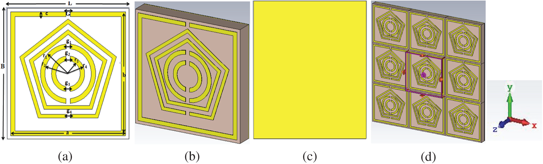
Figure 1: (a) Labeled unit cell, (b) perspective view of the unit cell, (c) bottom copper, and (d) simulation setup

The unit cell of the proposed MA was simulated using a high-performance 3D electromagnetic field simulation software computer simulation technology (CST). The unit cell boundary is applied to the x and y directions while electromagnetic radiation is propagated through the z direction. Two floquet and waveguide ports were placed at the +z and –z ends of the z-axis. An incident electromagnetic wave propagated to the unit cell boundary could generate reflection, transmission, and absorption. The surface EM wave gets stimulated at the interface of the medium. Once stimulated, the surface electrons of the medium and the photons of the incident EM wave interact with each other to exponentially decrease the transmission depth and constrain the energy of part of the EM wave. The reflection intensity declines when the frequency of the incident EM wave is closer to the resonance frequency of the surface plasma of the medium. Hence, the radiation energy is absorbed by the medium [30]. The reflection and transmission coefficients are the two essential parameters used to estimate the absorption efficiency A(ω) of any MA. These three parameters are expressed by Eq. (1) [31,32].
The other two parameters, transmission efficiency and reflection efficiency, will be minimased shown by Eq. (2) to achieve maximum MA efficiency.
The bottom copper sheet with the appropriate thickness of the unit cell is sufficient to block the transmission of the incident EM wave. The absorption efficiency A(ω) only depends on the reflection efficiency R(ω).
The EM properties of an MA depend on its charge, which is responsible for the different fields and forces. The Maxwell’s curl equations describe the induced electric and magnetic fields [33].
Here, H = Magnetic field intensity (Am−1), D = Electric flux density and its unit is (Cm−2).
and del operator,
To eradicate the limitations of the Eqs. (4)–(7) can be used [34].
ε and µ represent the material properties where ε = permittivity (F/m) and µ = permeability (H/m).
To investigate physical properties and to estimate the power loss of the unit cell FIT based CST microwave is used. The substandard dielectric layer solidly subject to the parameters loss-tangent value as tanδ = 0.025.
Fig. 2 demonstrates the CST simulated results for the reflection coefficient (S11), transmission coefficient (S21), and absorptivity value. The unit cell exhibits three resonance peaks of absorption, 96.82%, 99.42%, and 99.13%, at the resonance frequencies of 6.85, 8.87, and 12.03 GHz, respectively. The transmission coefficient (S21) was estimated to be zero as the bottom copper successfully constrained the transmission of incident radiation. Based on the observation, the suggested PMA exhibited negative epsilon and negative mu properties, i.e., DNG characteristics, as demonstrated in Fig. 3.
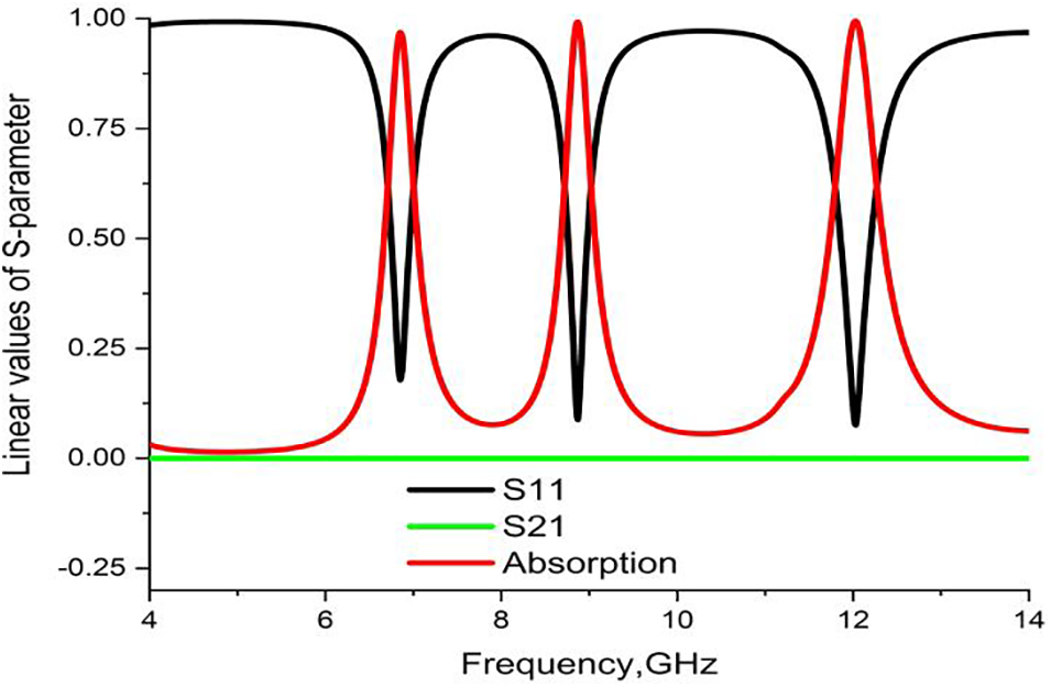
Figure 2: Graphical view of the reflection coefficient (S11), transmission coefficient (S21), and absorption of the proposed absorber
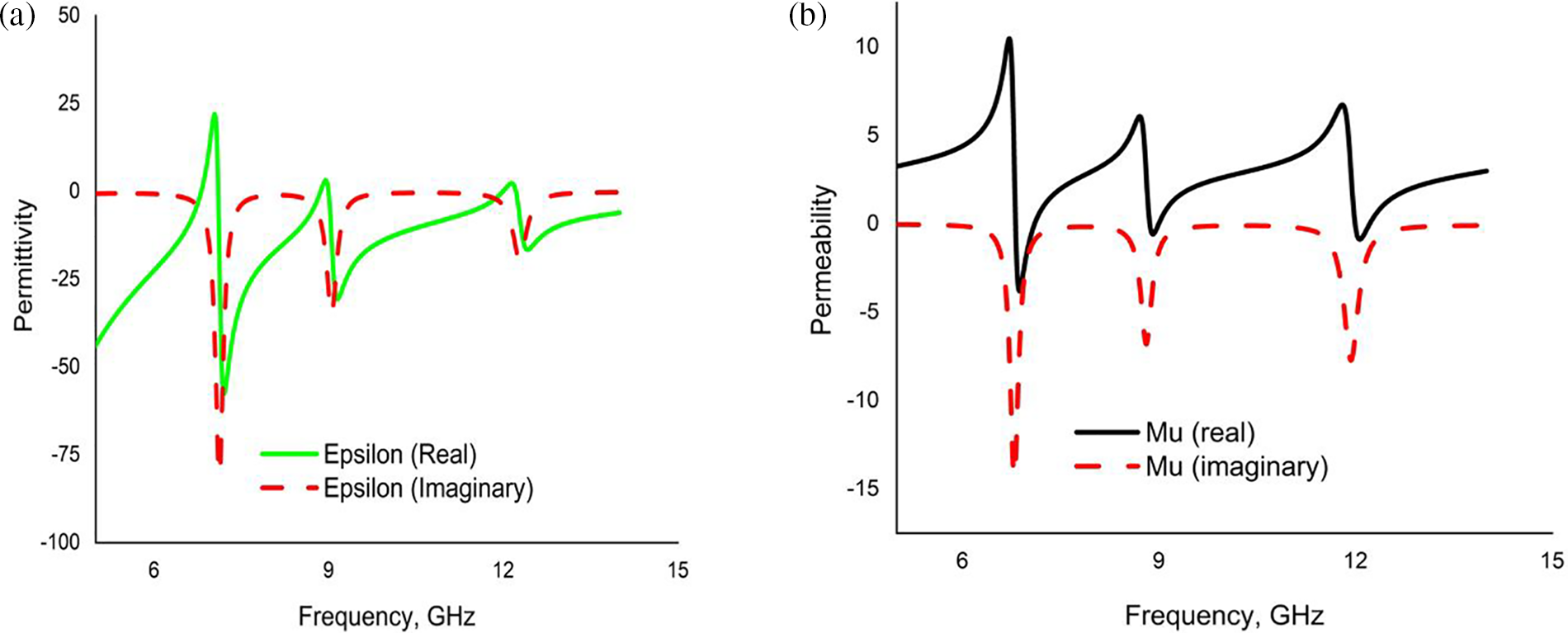
Figure 3: (a) Permittivity (real and imaginary), (b) Permeability (real and imaginary)
The average absorption of a MA can be calculated by using Eq. (8) [35].
where, A(λ) = absorption at a specific wavelength, λu = upper frequency, and λL= lower frequency.
This section also discusses the dependency of polarisation and incident angles. These observations are essential to ensure the universal application of any MA.
Meanwhile, Fig. 4 depicts the CST results of absorption for different polarisation angles in transverse electric mode (TE).
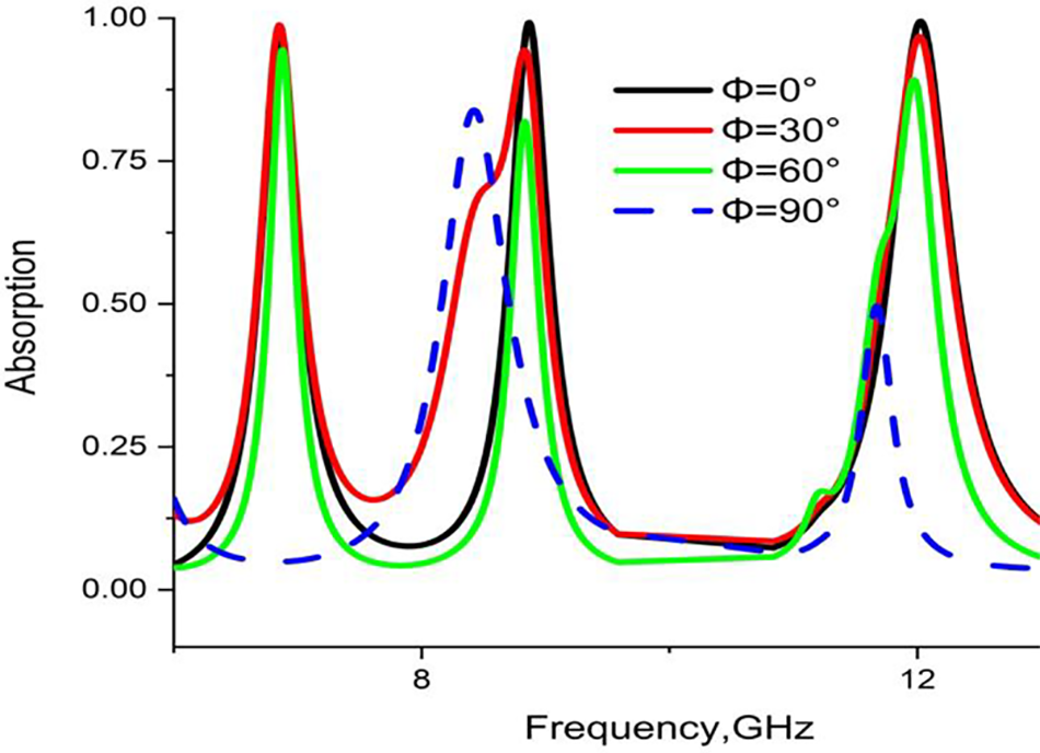
Figure 4: CST results of absorption at different polarisation angles
For the polarisation angle, Φ = 0° at normal incidence, the proposed MA yielded maximum absorbance of 96.82%, 99.24%, and 99.43% at 6.85, 8.87, and 12.03, respectively. The polarisation angle for Φ = 30° at a normal incident angle also exhibited three major resonance peaks at 6.85, 8.84, and 12.02 GHz with an absorption of 98.82%, 95.68%, and 96.73%, respectively. Similarly, Φ = 60° generated three resonance frequencies at 6.85, 8.44, and 11.98 GHz with an absorbance of 94.26%, 81.94%, and 89.19%, respectively. Lastly, for the pol. angle Φ = 90° at normal incidence yielded dual resonance peaks at 8.42 and 11.67 GHz, indicating consecutive polarisation angles and absorbance rates discrepancies compared to the other readings. Therefore, the proposed PMA is polarisation insensitive up to 60°.
Besides that, the absorbance efficiency of the proposed PMA was also observed for various oblique incidence angles. Fig. 5 demonstrates the absorption rates for oblique incident angles (θ) at 0°, 15°, 30°, 45°, and 60°. The progression of the incident angle to the right maintained the resonance frequency and the concerned absorption values as they remained almost unchanged. The proposed PMA can be treated as a broad oblique incident angle absorber for consistency using the same pattern up to 60°.
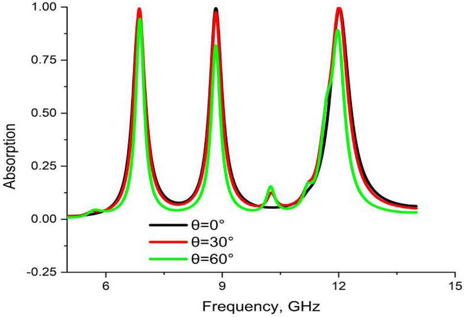
Figure 5: CST results of absorption at various oblique incident angles
The production of electric charge in the unit cell generates an electric field distribution, magnetic field distribution, and surface current, as illustrated in Figs. 6–8, respectively. These fields were inspected to determine the absorption mechanism of the PMA. Different parts of the unit cell are influenced by the change of current flow observed at three resonance frequencies (6.85, 8.87, and 12.03 GHz). Maxwell curl equations can be used to explain the reasons and causes of induced electric and magnetic fields. This section of the current study demonstrates the behaviours and patterns of the fields and the specific contribution of each part of the unit cell. For the starting frequency of 6.85 GHz, the charges in the square ring and pentagon resonators gradually move clockwise (left to right). The surface current in the ground metallic layer is the reverse of the top resonator layer. This anti-parallel current flow resulted in the magnetic resonance responsible for EM absorption. A massive quantity of (+)ve and (−)ve charges congregated at the two reverse ends of the concerned resonators generated a strong electric field.
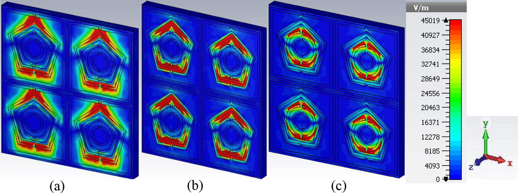
Figure 6: Electric field distribution at (a) 6.85 GHz (b) 8.87 GHz (c) 12.03 GHz
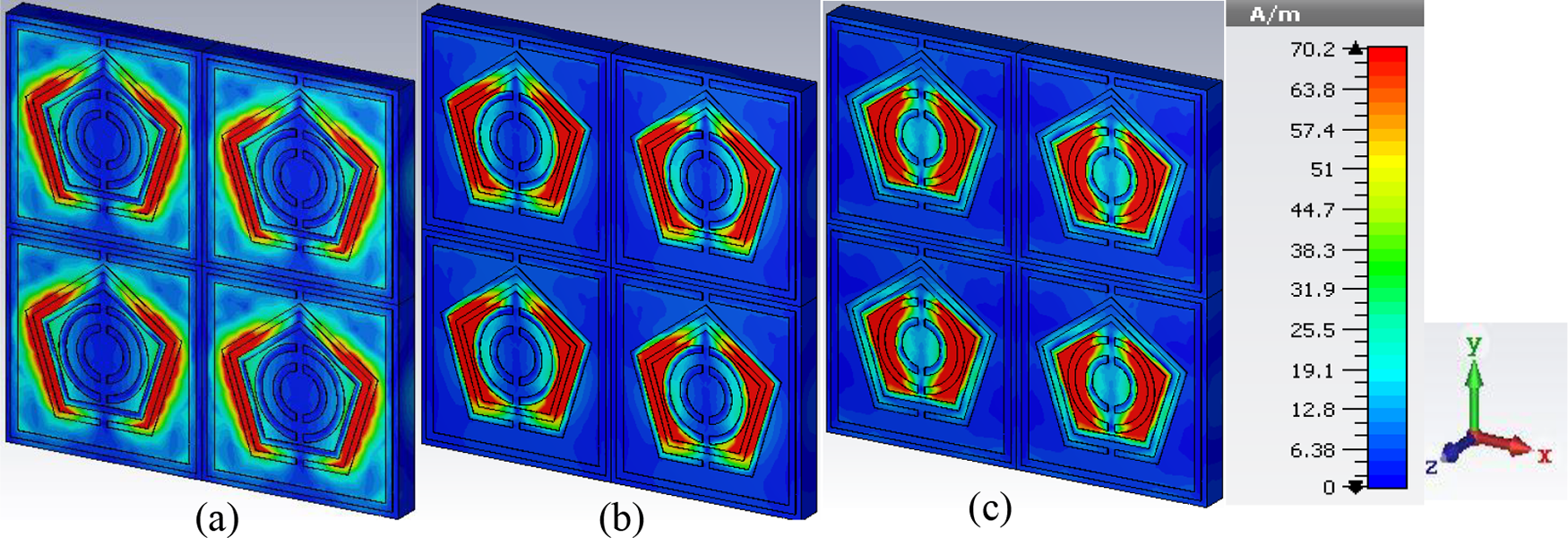
Figure 7: Magnetic field distribution at (a) 6.85 GHz (b) 8.87 GHz (c) 12.03 GHz

Figure 8: Surface current distribution at (a) 6.85 GHz (b) 8.87 GHz (c) 12.03 GHz
On the other hand, strong magnetic dipoles were generated in the two pentagons for accumulating (+)ve and (−)ve charges at the two reverse ends of the pentagons for a frequency of 8.87 GHz. As for the third resonance frequency of 12.03 GHz, a magnetic field was induced due to the magnetic resonance in the inverse C-shaped and the intermediate medium layer. In brief, the dissemination of the two fields was vividly distinct and continued across the designed unit cell of the MA. Three resonance frequencies influence the different parts of the resonators. As the electric and magnetic fields were applied to the x- and y-axes, two field distributions that were perpendicular to each other were formed, as depicted in Figs. 6 and 7. The direction of the electric field was strongly related to the surface current distribution while the intensity of the surface current in a different resonator segment was reinforced by the bottom plane recently responsible for the double negative (−ε & −µ) characteristics. This exotic property of the proposed PMA resulted in a negative refractive index. In short, the clockwise and anti-clockwise electric flows at various resonance frequencies generated magnetic dipoles responsible for the absorption of incident EM radiation.
Table 2 briefly describes the relative statement of published MAs with the proposed PMA. The suggested PMA is more expedient for dynamic characteristics such as absorptivity, unit cell size and shape, and the band covering compared to the six published six contemporary articles.

3.1 Design Selection Procedure and Parametric Study
Fig. 9 illustrates the different stages of optimisation of the presented PMA. The best design was selected through the trial and error technique to yield the expected outcome [42]. Furthermore, the unit cell was finalised by investigating the surface current that causes the fluctuation of the resonance frequency. The unit cell was designed by placing an SRR and a PSRR of the same width (0.40 mm) on the substrate layer (Fig. 9a). The CST results indicated one resonance peak at 6.69 GHz with an absorbance of 93.32%. Meanwhile, an additional PRR of a comparatively smaller size was placed on the inside of the design-i, as depicted in Fig. 9b. The numerical simulation revealed a dual resonance peak at 6.84 and 8.88 GHz with an absorptivity of 96.49% and 99.62%, respectively. Fig. 9c combines two inverse C-shaped resonators with that of Fig. 8b to yield three resonance peaks at 6.83, 8.79, and 12.01 GHz with absorptions of 96.73%, 99.32%, and 98.13%, respectively. Moreover, two small inverse C-shaped resonators were also placed at the centre of Fig. 9c design as illustrated in Fig. 9d. Upon adding the two small inverse C-shaped resonators, numerical simulations of this unit cell structure also yielded three resonance peaks at 6.85, 8.87, and 12.03 GHz with absorption of 96.82%, 99.42%, and 99.13%, respectively. These values were congruent with the targeted frequency range with good absorption value. Fig. 9e represents the CST results of absorption for all designs of the proposed MA.
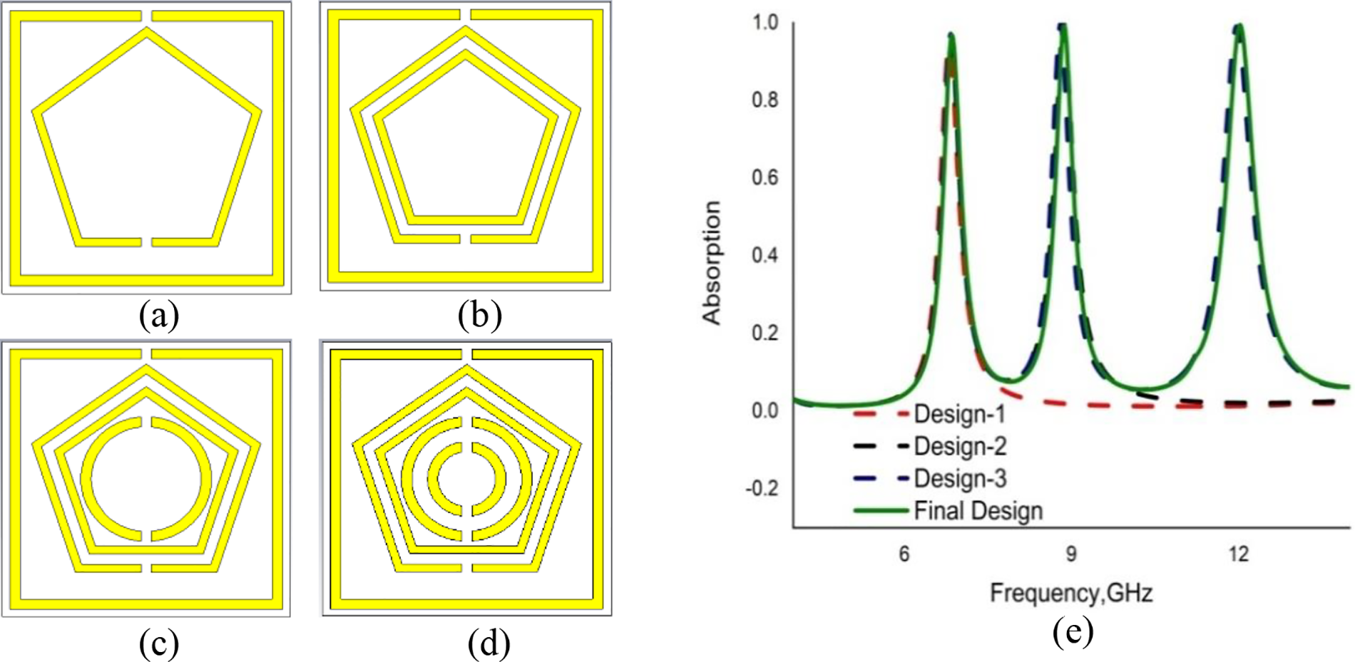
Figure 9: Design selection stages and simulated results (a) Design-1, (b) Design-2, (c) Design-3, (d) Final Design, and (e) CST simulated absorption results for design (a–d)
A study was conducted to observe the performance of the proposed MA with the change of widths and split gaps of different metallic resonators. The widths of the resonators were maintained at 0.60, 0.50, and 0.40 mm, to investigate the resonance frequencies along with the absorption rates. Of the three widths, 0.40 mm width yielded the best performance, with resonance frequencies at 6.85, 8.87, and 12.03 GHz and absorption rates of 96.82%, 99.24%, and 99.43%, respectively (Fig. 10a). Meanwhile, the split gaps of different resonators take into account the changing absorption patterns at other split gaps. The simulated results for the varying split gaps, 0.30, 0.40, and 0.50 mm were inspected, whereby 0.40 mm yielded the maximum performance. Fig. 10 depicts the simulated widths and split gaps results. The lower frequencies gradually shift to higher readings with the increase of split gap. (Fig. 10b). Moreover, the widths of the two inverse C-shaped resonators indicated that the 0.40 mm width of the resonator was the most responsive which is depicted in the Fig. 10c.
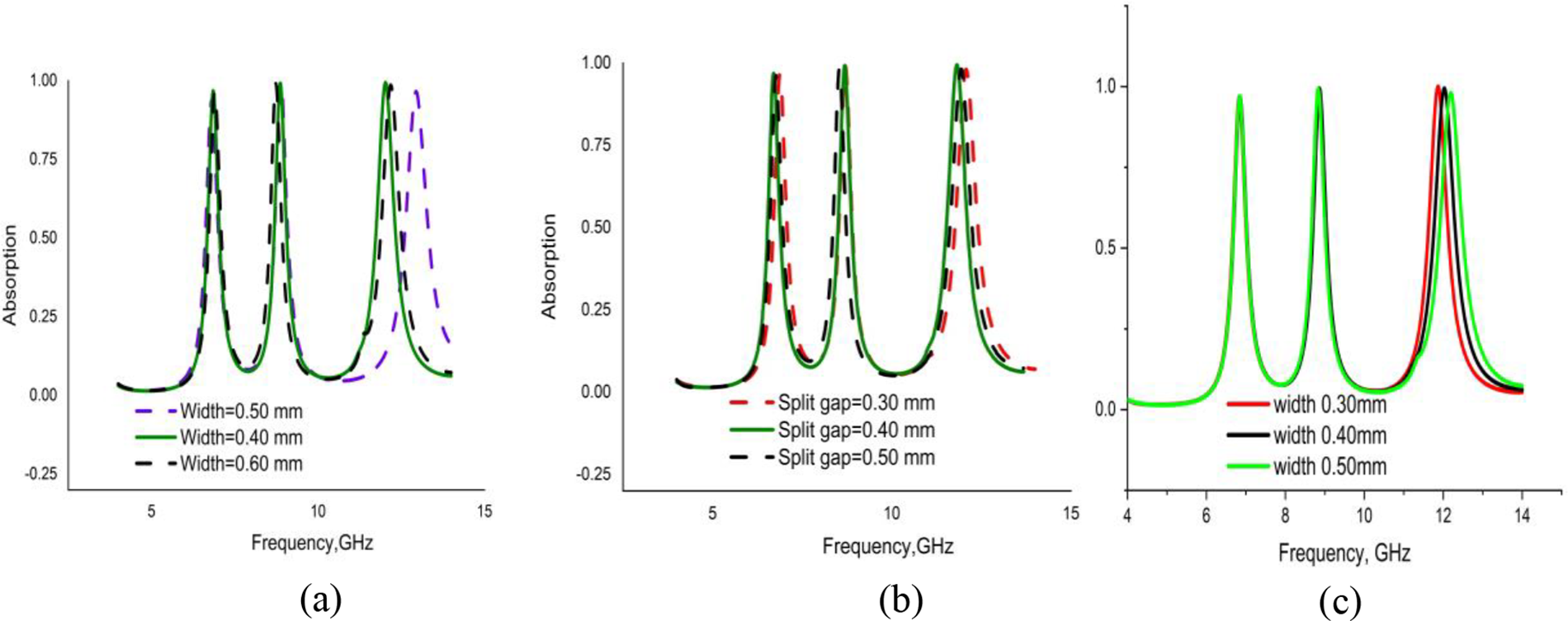
Figure 10: Absorption rate at (a) changing widths of SRR & pentagons, (b) changing split gaps and (c) changing widths of the C-shaped resonator
3.2 Validating Numerical Results of the Proposed PMA
The metallic upper layer of the proposed unit cell of MA is an arrangement of differently shaped metallic structures with some split gaps. Every gap in the resonator plays the capacitor role, whereas every metal bar represents an inductor. Hence, the complete PMA is represented by an electrical circuit that combines some inductors and capacitors [43]. The proposed unit cell structure is an electrical LC resonance circuit, as illustrated in Fig. 11a. Fig. 11b illustrates the reflection coefficient (S11) of the advanced design system (ADS).
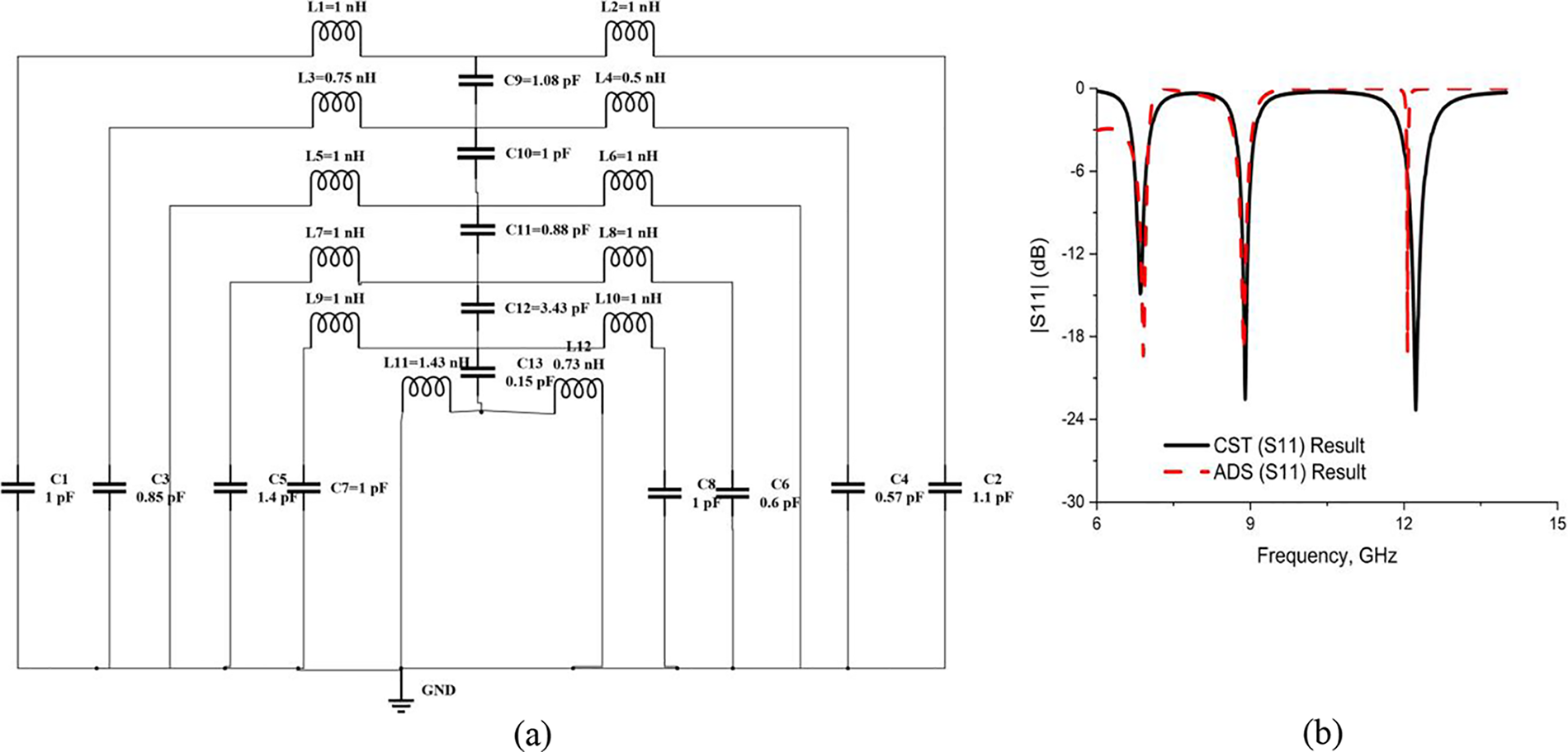
Figure 11: (a) Equivalent electrical LC circuit with the values of L & C, and (b) Comparison of reflection coefficient (S11) for CST and ADS results
If an inductor’s inductance is L and a capacitor’s capacitance is C, then the resonance frequency (f) can be determined from Eq. (9) [44].
where, f is used for frequency (Hz), C for capacitance (F), and L for inductance (H-Henry) of the respective LC resonance circuit.
The capacitance within a split gap d generated by a capacitor can be derived using Eq. (10).
Here, ϵ0 refers to permittivity in free space, ϵr for relative permittivity, A for cross-sectional area (m2), and C for capacitance (F-Farad).
Eq. (11) calculates the inductance of an inductor in the circuit [45].
where, Kg is the correction factor, while w, l, and t refer to the width, length, and thickness, respectively.
The projected PMA is a congress of metal and dielectric components. The electrical LC circuit of the presented PMA unit cell is demonstrated in Fig. 10, where L1 to L12 refer to the inductors and C1 to C13 represent the capacitors. The SRR of the PMA unit cell was exchanged by (L1, C1) and (L2, C2), while the first PSRR was represented by (L3, C3) and (L4, C4). The coupling capacitor C9 connected these two loops. Meanwhile, inductors L5 and L6 were placed for the second pentagonal resonator, with C10 being the connector capacitor. The (L7, C5) and (L8, C6) are the two bigger inverse C-shaped resonators. The two smaller inverse C-shaped resonators were represented by (L9, C7) and (L10, C8), with C11 and C12 being the coupling capacitors to connect the C-shapes with the smaller pentagon. The thin bottom copper layer was represented by inductors L11 and L12. The bottom layer was coupled with an upper metallic layer via a coupling capacitor C13. An equivalent electric circuit was simulated by ADS software exhibiting triple resonance peaks at 6.90, 8.86, and 12.07 GHz with the magnitudes of −19.38, −18.53, and −19.10 dB, respectively. The simulated CST and ADS results were identical, as depicted in Fig. 11b.
On the other hand, the finite element method-based analysis system software HFSS was used to validate the results of the proposed PMA. The HFSS simulated result also yielded three resonance peaks at 7.01, 8.92, and 12.33 GHz with absorption rates of 95.37%, 96.09%, and 96.68%, respectively. The CST simulated results exhibited better homogeneity with the HFSS, as depicted in Fig. 12.
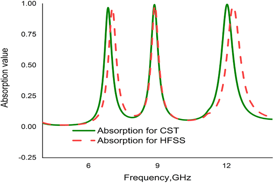
Figure 12: Absorption results for CST and HFSS simulations
Different types of array combinations were investigated to assess the structural imperfections and coupling effects of the proposed MA. High-performance 3D EM field simulator CST also simulated various arrays of the proposed MA. The unit cell is kept as a boundary condition in the direction of the x- and y-axes, while the EM wave was propagated parallel to the z-axis. This mechanism also generated three phenomena, namely reflection, transmission, and absorption. The 1 × 2 array yielded triple resonance peaks at 6.88, 9.07, and 12.42 GHz with absorption rates of 96.13%, 99.10%, and 98.10%, respectively.
Meanwhile, arrays 2 × 2 and 8 × 8 exhibited approximately the same results, which were in good agreement with the CST results of the unit cell. Fig. 13 compares the absorption results of the different arrays with the unit cell of the designed PMA. The coupling effects were observed for the 1 × 2 array where the resonance frequencies shifted slightly to the right.
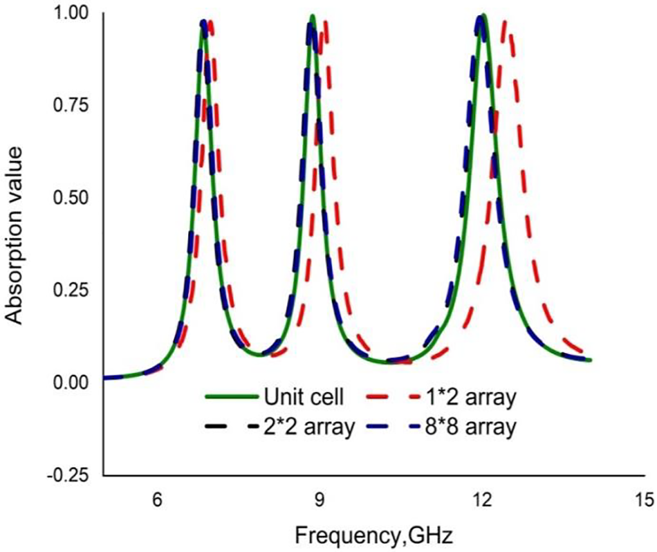
Figure 13: Absorption results for different arrays and unit cell
This study offers a royal crown-shaped triple band polarisation insensitive PMA. The numerical simulation exhibited three resonance peaks at 6.85, 8.87, and 12.03 GHz with near-unity absorbance. The C-, X- and Ku-bands MA demonstrated polarisation insensitiveness up to 60° and oblique incident angle up to 60°. The proposed MA was inspected with authentication processes, namely an equivalent circuit model and HFSS. The electric field, magnetic field, and surface current were analysed to understand the absorption mechanism. Important and significant characteristics of the proposed PMA were inspected in the parametric discussion section which deliberates the impression of vibrant tuning within the expected bands. Additionally, the proposed MA exhibited practical viability in terms of the compactness of the structure, λ/4 = 10.95 mm (calculated at the lower frequency, 6.85 GHz). This unique novel geometric structure of the presented PMA adapted some endorsement procedures that led to its eccentricity. The simple outlook and standard configuration of the proposed PMA are advantageous for simple implementation compared to the contemporary published MA. Although some design configuration problems might limit its symmetry, such limitations can be solved during the MA sensor applications in the future. In brief, the outcome of this study can be adopted in satellite communication band applications, defence and security, stealth and coating technology.
Acknowledgement: This work was supported by Fundamental Research Grant Scheme (FRGS), MOE, Malaysia, Code: FRGS/1/2022/TK07/UKM/02/22. The authors also acknowledge with thanks to the ICT division, Ministry of Posts, Telecommunications and Information Technology, Bangladesh, under the code: 1280101-120008431-3821117 to support the research work.
Funding Statement: This work was supported by Fundamental Research Grant Scheme (FRGS), MOE, Malaysia, Code: FRGS/1/2022/TK07/UKM/02/22.
Conflicts of Interest: The authors declare that they have no conflicts of interest to report regarding the present study.
References
1. R. A. Shelby, D. R. Smith and S. Schultz, “Experimental verification of a negative index of refraction,” Science, vol. 292, pp. 77–79, 2001. [Google Scholar] [PubMed]
2. D. R. Smith, W. J. Padilla, D. C. Vier, S. C. Nemat-Nasser and S. Schultz, “Composite medium with simultaneously negative permeability and permittivity,” Physical Review Letters, vol. 84, no. 18, pp. 4184–4187, 2000. [Google Scholar] [PubMed]
3. F. B. P. Niesler, J. K. Gansel, S. Fischbach and M. Wegener, “Metamaterial metal-based bolometers,” Applied Physics Letters, vol. 100, no. 20, pp. 203–508, 2012. [Google Scholar]
4. D. Wu, R. Li, Y. Liu, Z. Yu, L. Yu et al., “Ultra-narrow band perfect absorber and its application as plasmonic sensor in the visible region,” Nanoscale Research Letters, vol. 12, no. 1, pp. 1–11, 2017. [Google Scholar]
5. K. V. Sreekanth, Y. Alapan, M. ElKabbash, E. Ilker, M. Hinczewski et al., “Extreme sensitivity biosensing platform based on hyperbolic metamaterials,” Nature Materials, vol. 15, no. 6, pp. 621–627, 2016. [Google Scholar] [PubMed]
6. Y. Zhang, H. Zhang, D. Chen, C. J. Sun, Y. Ren et al., “Engineering of exciton spatial distribution in CdS nanoplatelets,” Nano Letters, vol. 21, no. 12, pp. 5201–5208, 2021. [Google Scholar] [PubMed]
7. N. I. Landy, S. Sajuyigbe, J. J. Mock, D. R. Smith, W. J. Padilla et al., “Perfect metamaterial absorber,” Physical Review Letters, vol. 100, no. 20, pp. 207–402, 2008. [Google Scholar]
8. L. Huang and H. Chen, “Multi-band and polarization insensitive metamaterial absorber,” Progress in Electromagnetics Research, vol. 113, pp. 103–110, 2011. [Google Scholar]
9. Q. Y. Wen, H. W. Zhang, Y. S. Xie, Q. H. Yang and Y. L. Liu, “Dual band terahertz metamaterial absorber: Design, fabrication, and characterization,” Applied Physics Letters, vol. 95, no. 24, pp. 241111, 2009. [Google Scholar]
10. H. Tao, A. C. Strikwerda, K. Fan, C. M. Bingham, W. J. Padilla et al., “Terahertz metamaterials on free-standing highly-flexible polyimide substrates,” Journal of Physics D: Applied Physics, vol. 41, no. 23, pp. 232004, 2008. [Google Scholar]
11. W. Zhu, X. Zhao, B. Gong, L. Liu and B. Su, “Optical metamaterial absorber based on leaf-shaped cell,” Applied Physics A, vol. 102, no. 1, pp. 147–151, 2010. [Google Scholar]
12. C. Hu, Z. Zhao, X. Chen and X. Luo, “Realizing near-perfect absorption at visible frequencies,” Optics Express, vol. 17, no. 13, pp. 11039, 2009. [Google Scholar] [PubMed]
13. T. Maier and H. Brückl, “Wavelength-tunable microbolometers with metamaterial absorbers,” Optics Letters, vol. 34, no. 19, pp. 3012, 2009. [Google Scholar] [PubMed]
14. G. Deng, K. Lv, H. Sun, J. Yang, Z. Yin et al., “An ultrathin, triple-band metamaterial absorber with wide-incident-angle stability for conformal applications at X and Ku frequency band,” Nanoscale Research Letters, vol. 15, no. 1, pp. 1010, 2020. [Google Scholar]
15. T. Ramachandran, M. R. I. Faruque, E. Ahamed and S. Abdullah, “Specific absorption rate reduction of multi split square ring metamaterial for L- and S-band application,” Results in Physics, vol. 15, pp. 102–668, 2019. [Google Scholar]
16. K. S. Al-badri, “Multi band metamaterials absorber for stealth applications,” Law, State and Telecommunications Review, vol. 11, no. 1, pp. 133–144, 2019. [Google Scholar]
17. S. Hannan, M. T. Islam, M. R. I. Faruque and H. Rmili, “Polarization-independent perfect metamaterial absorber for C, X and, Ku band applications,” Journal of Materials Research and Technology, vol. 15, pp. 3722–3732, 2021. [Google Scholar]
18. Z. Zhang, L. Zhang, X. Chen, Z. Wu, Y. He et al., “Broadband metamaterial absorber for low-frequency microwave absorption in the S-band and C-band,” Journal of Magnetism and Magnetic Materials, vol. 497, no. 1, pp. 66–75, 2020. [Google Scholar]
19. D. Yang and Y. Xia, “Experimental verification of multi-band metamaterial absorber with double structured layers,” Materials Research Express, vol. 7, no. 3, pp. 1–8, 2020. [Google Scholar]
20. Y. J. Kim, Y. J. Yoo, K. W. Kim, J. Y. Rhee, Y. H. Kim et al., “Dual broadband metamaterial absorber,” Optics Express, vol. 23, no. 4, pp. 3861, 2015. [Google Scholar] [PubMed]
21. Y. Wu, X. Ding and B. Wang, “A dual-band broadband metamaterial absorber with wide-angle absorption and polarization insensitivity,” in Int. Conf. on Microwave and Millimeter Wave Technology (ICMMT), Chengdu, China, pp. 1–3, 2018. [Google Scholar]
22. M. Amiri, F. Tofigh, N. Shariati, J. Lipman and M. Abolhasan, “Wide-angle metamaterial absorber with highly insensitive absorption for TE and TM modes,” Scientific Reports, vol. 10, no. 1, pp. 13638, 2020. [Google Scholar] [PubMed]
23. M. R. Islam, M. T. Islam, M. Moniruzzaman, M. Samsuzzaman and H. Arshad, “Penta band single negative meta-atom absorber designed on square enclosed star-shaped modified split ring resonator for S-, C-, X- and Ku-bands microwave applications,” Scientific Reports, vol. 11, no. 1, pp. 1–22, 2021. [Google Scholar]
24. X. Niu, D. Qi, X. Wang, Y. Cheng, F. Chen et al., “Improved broadband spectral selectivity of absorbers/emitters for solar thermophotovoltaics based on 2D photonic crystal heterostructures,” Journal of the Optical Society of America A, vol. 35, no. 11, pp. 1832–1838, 2018. [Google Scholar]
25. C. M. Watts, X. Liu and W. J. Padila, “Metamaterial electromagnetic wave absorbers,” Advanced Mater, vol. 24, no. 23, pp. OP89–OP180, 2012. [Google Scholar]
26. M. J. Park, J. Choi and S. S. Kim, “Wide bandwidth pyramidal absorbers of granular ferrite and carbonyl iron powders,” IEEE Transactions Magnetics, vol. 36, no. 5, pp. 3272–3274, 2000. [Google Scholar]
27. Y. Cheng, Z. Cheng, X. Mao and R. Gong, “Ultra-thin multi-band polarization-insensitive microwave metamaterial absorber based on multiple-order responses using a single resonator structure,” Materials, vol. 10, no. 11, pp. 12–41, 2017. [Google Scholar]
28. Y. Zhou, Z. Qin, Z. Liang, D. Meng, H. Xu et al., “Ultra-broadband metamaterial absorbers from long to very long infrared regime,” Light, Science & Applications, vol. 10, no. 1, pp. 138, 2021. [Google Scholar]
29. S. Kalraiya, R. K. Chaudhary and M. A. Abdalla, “Resistor loaded wideband conformal metamaterial absorber for curved surfaces application,” AEU—International Journal of Electronics and Communications, vol. 143, no. 1, pp. 154033, 2022. [Google Scholar]
30. S. A. Ali, M. Abu, S. N. Zabri and S. A. Hamzah, “Wide-band metamaterial perfect absorber through double arrow shape printed on a thin dielectric,” Bulletin of Electrical Engineering and Informatics, vol. 10, no. 5, pp. 2488–2495, 2021. [Google Scholar]
31. Z. Xiong and L. Cao, “Tailoring morphology, enhancing magnetization and photocatalytic activity via Cr doping in Bi25FeO40,” Journal of Alloys and Compounds, vol. 773, pp. 828–837, 2019. [Google Scholar]
32. X. Luo, X. Zhai, L. L. Wang and Q. Lin, “Enhanced dual-band absorption of molybdenum disulfide using plasmonic perfect absorber,” Optics Express, vol. 26, no. 9, pp. 11658–11666, 2018. [Google Scholar] [PubMed]
33. M. S. U. Afsar, M. R. I. Faruque, M. B. Hossain, A. M. Siddiky, M. U. Khandaker et al., “A new octagonal close ring resonator based dumbbell-shaped tuning fork perfect metamaterial absorber for C- and Ku-band,” Micromachine, vol. 13, no. 2, pp. 162, 2022. [Google Scholar]
34. M. Lobet, M. Lard, M. Sarrazin, O. Deparis and L. Henrard, “Plasmon hybridization in pyramidal metamaterials: A route towards ultra-broadband absorption,” Optics Express, vol. 22, no. 10, pp. 12678–12690, 2014. [Google Scholar] [PubMed]
35. E. Ahamed, M. R. I. Faruque, M. F. Mansor and M. T. Islam, “Polarization-dependent tunneled metamaterial structure with enhanced fields properties for X-band application,” Results in Physics, vol. 15, no. 1, pp. 102530, 2019. [Google Scholar]
36. M. Agarwal, A. K. Behera and M. K. Meshram, “Dual resonating C-band with enhanced bandwidth and broad X-band metamaterial absorber,” Applied Physics A, vol. 122, no. 166, pp. 1–9, 2016. [Google Scholar]
37. M. S. Sim, K. Y. You, F. Esa, M. N. Dimon and N. H. Khamis, “Multiband metamaterial microwave absorbers using split ring and multiwidth slot structure,” International Journal of RF and Microwave Computer-Aided Engineering, vol. 28, no. 7, pp. 214–473, 2018. [Google Scholar]
38. R. K. Singh and A. Gupta, “A wrenched-square shaped polarization independent and wide angle stable ultra-thin metamaterial absorber for S-band, X-band and Ku-band applications,” AEU—International Journal of Electronics and Communications, vol. 132, pp. 153648, 2021. [Google Scholar]
39. M. F. Zafar and U. Masud, “A multiple-bands metamaterial absorber based in X, Ku and K-band,” Research Square, vol. 10, no. 21203, pp. 1–10, 2021. [Google Scholar]
40. S. Kalraiya, R. K. Chaudhary and R. K. Gangwar, “Polarization independent triple band ultrathin conformal metamaterial absorber for C- and X-frequency bands,” AEU International Journal of Electronics and Communications, vol. 135, pp. 153752, 2021. [Google Scholar]
41. S. Habib, G. Iqbal Kiani, M. Fasih Uddin Butt, S. Muzahir Abbas, A. Jeza Aljohani et al., “Ultra-wideband frequency selective surface for communication applications,” Computers, Materials & Continua, vol. 70, no. 3, pp. 6177–6187, 2022. [Google Scholar]
42. M. T. Islam, M. R. I. Faruque and N. Misran, “Specific absorption rate analysis using metal attachment,” Informacije MIDEM, vol. 40, no. 3, pp. 238–240, 2010. [Google Scholar]
43. A. Hoque, M. Tariqul Islam, A. F. Almutairi, T. Alam, M. Jit Singh et al., “A polarization independent quasi-TEM metamaterial absorber for X and Ku band sensing applications,” Pubmed, vol. 18, no. 12, pp. 4209, 2018. [Google Scholar]
44. M. S. U. Afsar, M. R. I. Faruque, M. B. Hossain, M. T. Islam, M. U. Khandaker et al., “Tuning fork-hammer shaped perfect metamaterial absorber for C-band applications,” Radiation Physics and Chemistry, vol. 200, pp. 110262, 2022. [Google Scholar]
45. G. Kaur and A. Kaur, “Breast tissue tumor detection using “S” parameter analysis with an UWB stacked aperture coupled microstrip patch antenna having a “+” shaped defected ground structure,” International Journal of Microwave and Wireless Technologies, vol. 12, no. 7, pp. 1–17, 2020. [Google Scholar]
Cite This Article
 Copyright © 2023 The Author(s). Published by Tech Science Press.
This work is licensed under a Creative Commons Attribution 4.0 International License , which permits unrestricted use, distribution, and reproduction in any medium, provided the original work is properly cited.
 Downloads
 Citation Tools