
 Submit a Paper
 Propose a Special lssue
 Open Access
ARTICLE
Void Formation Analysis in the Molded Underfill Process for Flip-Chip Packaging
1 Department of Mold and Die Engineering, National Kaohsiung University of Science and Technology, Kaohsiung, 807, Taiwan
2 Product Characterization, Corporate R&D, Advanced Semiconductor Engineering, Inc., Kaohsiung, 811, Taiwan
* Corresponding Author: Ian Hu. Email:
(This article belongs to the Special Issue: Selected Papers from the International Multi-Conference on Engineering and Technology Innovation 2024 (IMETI2024))
Computers, Materials & Continua 2025, 84(1), 537-551. https://doi.org/10.32604/cmc.2025.065330
Received 10 March 2025; Accepted 27 April 2025; Issue published 09 June 2025
 View Full Text
 Download PDF
Abstract
Flip-chip technology is widely used in integrated circuit (IC) packaging. Molded underfill transfer molding is the most common process for these products, as the chip and solder bumps must be protected by the encapsulating material to ensure good reliability. Flow-front merging usually occurs during the molding process, and air is then trapped under the chip, which can form voids in the molded product. The void under the chip may cause stability and reliability problems. However, the flow process is unobservable during the transfer molding process. The engineer can only check for voids in the molded product after the process is complete. Previous studies have used fluid visualization experiments and developed computational fluid dynamics simulation tools to investigate this issue. However, a critical gap remains in establishing a comprehensive three-dimensional model that integrates two-phase flow, accurate venting settings, and fluid surface tension for molded underfill void evaluation—validated by experimental fluid visualization. This study aims to address this gap in the existing literature. In this study, a fluid visualization experiment was designed to simulate the transfer molding process, allowing for the observation of flow-front merging and void formation behaviors. For comparison, a three-dimensional mold flow analysis was also performed. It was found that the numerical simulation of the trapped air compression process under the chip was more accurate when considering the capillary force. The effect of design factors is evaluated in this paper. The results show that the most important factors for void size are fluid viscosity, the gap height under the chip, transfer time, contact angle between the fluid and the contact surfaces, and transfer pressure. Specifically, a smaller gap height beneath the chip aggravates void formation, while lower viscosity, extended transfer time, reduced contact angle, and increased transfer pressure are effective in minimizing void size. The overall results of this study will be useful for product and process design in selecting appropriate solutions for IC packaging, particularly in the development of void-free molded-underfill flip-chip packages. These findings support the optimization of industrial packaging processes in semiconductor manufacturing by guiding material selection and process parameters, ultimately enhancing package reliability and yield.Keywords
Plastic packaging is the mainstream approach in integrated circuit (IC) packaging, primarily aimed at protecting electronic devices using plastic encapsulating materials [1–5]. The most commonly used encapsulation process is transfer molding [6,7]. During this process, components such as chips, passive devices, and substrates are inserted into the mold cavity. However, the presence of these inserted components creates an uneven mold flow front [8]. Consequently, flow-front merging often occurs during molding, leading to air entrapment in the mold cavity, which can result in voids in the molded product [8,9]. These voids may compromise the stability and reliability of molded IC products, particularly in flip-chip packaging [10,11].
International Business Machines Corporation (IBM) pioneered the flip-chip technique [12], which utilizes solder bumps to establish connections between the chips and substrates. These solder bumps play two roles: electrical connection and stress buffering [13–16]. Owing to the coefficient of thermal expansion (CTE) mismatch between the chip and substrate, an underfill material is typically used to fill the gap between the chip and substrate to protect the solder bumps [17]. For this type of packaging, recently stress [18–21], warpage [22–25], thermal performance [26–29], and filling voids [30–34] are the primary concerns for professionals in relevant industries. Focus on the filling process, filling voids are the most concern. Several underfill filling processes are available [17], and capillary underfill (CUF) is one of the most widely adopted techniques [30–32,35,36].
In the CUF process, a dispensing needle is used to apply an underfill material to the substrate adjacent to the chip. Capillary action then draws the material into the gap between the substrate and the chip. However, the CUF process has drawbacks, including a longer filling time, which affects production efficiency, and the need for low-viscosity materials to enhance flow. The strength and durability of low-viscosity materials may decrease after curing. To address these limitations, a molded underfill (MUF) process was developed [37].
MUF is a transfer molding process that fills the epoxy molding compound (EMC) around and beneath the chip in a single step. In addition to the standard MUF flip-chip package, an extended design known as exposed-die MUF (eMUF) has been developed for low-profile requirements [38]. Mold flow simulation is a powerful tool for evaluating molding processes. Chang et al. highlighted the necessity of three-dimensional (3D) modeling during the molding process [39]. Similarly, Lee et al. [40] employed 3D mold flow modeling and identified that air trapped in the mold cavity owing to merged flow fronts is a common phenomenon that can induce voids in molded products.
Void issues are not limited to flip-chip packages but also affect system-in-package (SiP) modules [33,34]. Voids may arise from filler clogging [41]; however, flow-front merging remains the most critical factor. Using a 3D mold flow simulation, Chen et al. [42] demonstrated that air pockets consistently formed beneath the chips. Choi et al. [43] simulated the MUF process using a two-phase flow-modeling technique. Wu et al. emphasized the significance of flow resistance due to air pressure in a mold flow simulation, suggesting the necessity of incorporating two-phase flow considerations [44]. In addition, Hsu et al. [45] underscored the importance of accurate venting settings in mold flow simulations.
Flow visualization is a widely used experimental method for validating simulation models [46–49]. Guo and Young [50] developed a two-dimensional (2D) simulation model combined with flow visualization experiments to evaluate void formation during the MUF process. However, none of these studies considered the impact of the capillary force in MUF simulations. Nevertheless, Guo and Young [51] noted that the surface tension of the working fluid played a critical role in evaluating void formation in the MUF process.
MUF is a type of transfer molding process, in which the primary driving force for resin flow is the applied transfer pressure. Consequently, capillary force has generally not been a key consideration in traditional modeling approaches. Most prior studies assumed that pressure-driven flow dominates, and thus neglected capillary effects. However, when the mold geometry includes regions with significantly different flow resistances—such as the narrow gaps beneath chips—the contribution of capillary force becomes more critical for accurately predicting void formation. This reveals a limitation in previous models and underscores the need for a more comprehensive approach, as proposed in this study. At present, limited research has been conducted to validate the potential influence of capillary force in such scenarios. If this factor is overlooked, void risk could be underestimated, particularly in the narrow gap regions critical to flip-chip packaging. This highlights the necessity of incorporating capillary effects into simulation models to improve prediction accuracy.
Based on previous studies, a critical gap exists in developing a comprehensive 3D model that integrates two-phase flow, accurate venting settings, and fluid surface tension for MUF void evaluation, complemented by experimental validation through fluid visualization. This study addresses this gap in the literature. Furthermore, this study evaluates several factors from the perspectives of product design, material properties, and process parameters. In the transfer molding process control, the most critical parameters are the filling time (which can be derived from the transfer velocity) and packing pressure, similar to those in the injection molding process [52]. Therefore, the key factors include fluid viscosity, the contact angle between the fluid and contact surfaces, transfer time, transfer pressure, and gap height beneath the chip.
2.1 Definition of Research Topic
In this study, a simplified fluid visualization experiment was designed to simulate the actual transfer molding process. A visualized mold was developed to represent the flow-front merging phenomenon beneath the chip gap. Silicone oil was used as the working fluid instead of an EMC. Abbott and Higgins [53] reported that the surface tension of curing epoxy decreases linearly with temperature, with a coefficient of −0.074 dyne · cm−1 · °C−1. At a typical molding temperature of 175°C, the estimated surface tension is approximately 29.75 dyne/cm. In comparison, the surface tension of the selected silicone oil is about 21.3 dyne/cm, which is reasonably close to that of EMCs. Although silicone oil does not exhibit the same rheological behavior as EMCs—such as shear-thinning—its viscosity can be precisely selected from a wide range to match that of EMCs under molding conditions. This makes it a practical substitute for flow visualization purposes. Similar substitution has also been adopted in prior studies [51], supporting its validity for qualitative analysis of flow behavior and void formation. This substitution allowed the observation of the flow behavior in the MUF process without considering the rheology of the EMC. Therefore, experiments were conducted at room temperature. In this fluid visualization experiment, the flow front and air pockets were observed. In addition, a 3D mold flow simulation was performed for comparison. This study aims to provide suggestions for accurately determining air pocket sizes using mold flow simulation. Building upon the validated modeling solution, sensitivity analyses were conducted to examine the influence of variations in several critical design factors; these analyses provide valuable insights that are particularly useful for qualitatively evaluating the relative impact of each key factor under investigation, especially when considered within the broader context of design optimization and performance prediction. Beyond the analytical results presented in this study, the simulation framework developed herein offers practitioners a flexible and robust tool; it enables them to conduct case-specific analyses tailored to their actual product geometries and material characteristics, thereby enhancing the applicability of the methodology across a wide range of engineering scenarios and facilitating more informed decision-making in real-world design processes.
2.2 Experimental Framework and Methodology
The fluid visualization experimental setup is shown in Fig. 1, and the dimensions of the visualization mold are shown in Fig. 2. The mold was designed with nine chip-like protruding objects, hereafter referred to as “chips”. Each chip measured 10 mm × 10 mm with a thickness of 1 mm. The chips are spaced 4 mm apart. A glass plate was placed over the mold to create a 0.1 mm gap between the chips and glass, replicating the flow space of the MUF process, with thinner gaps beneath the chips and thicker flow channels around them.
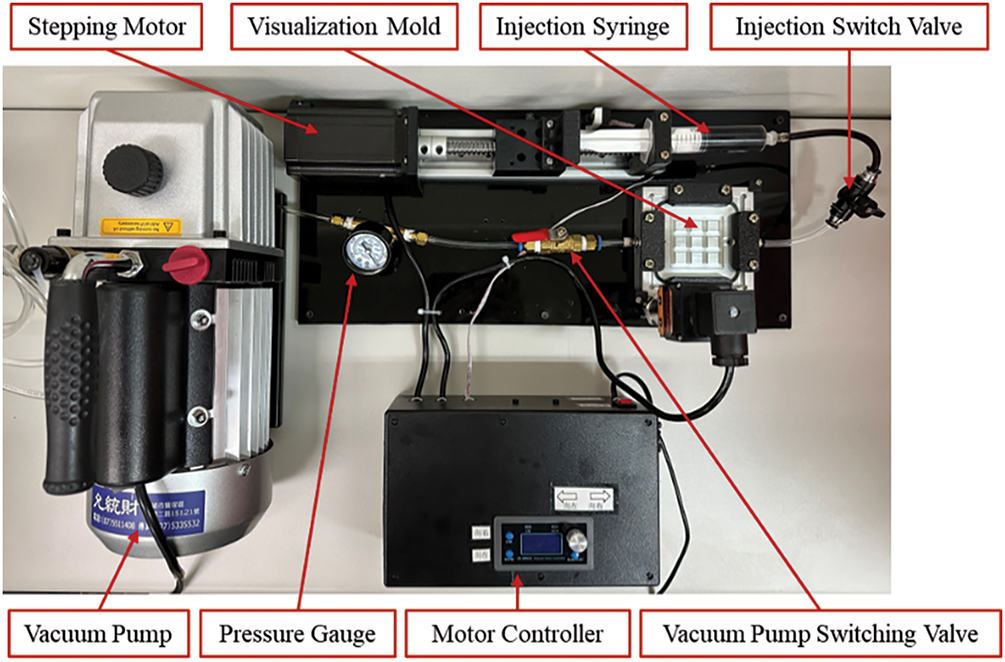
Figure 1: The fluid visualization experiment system

Figure 2: The dimension of the mold. Note: □ represents a square in geometry. Unit: mm
A stepping motor was used to transfer the working fluid from the syringe through the gate to the mold cavity. The presence of air creates flow resistance, leading to larger air pockets in the chip gap. To mitigate this, a high vacuum is preferred during molding. In this experiment, a vacuum pump was connected to the end opposite the gate to extract air and achieve a vacuum level of 19 kPa.
The viscosity of the working fluid significantly influences the flow behavior during the filling phase of the transfer molding process. For this reason, three silicone oils with different viscosities—1000, 3000, and 10,000 mPa · s—were selected for the experiments. The viscosities of silicone oil were selected based on the typical viscosity range of EMC during the encapsulation filling process. The filling process was captured using a high-speed camera to document the changes in the flow front. The captured images are shown in Fig. 3a. Edge detection was then applied as the image processing method to obtain a positional image of the flow front, as shown in Fig. 3b, with a particular focus on the air pockets in the chip gap. The experiment was conducted three times to ensure repeatability. The central air pocket was selected as the reference void for evaluation, and the results showed that the standard deviation of the void size was 2.43%, which is within an acceptable range for experimental repeatability.

Figure 3: The experimental image processing: (a) the image captured by a high-speed camera; (b) the image after image processing
2.3 Theory of Mold Flow Simulation
In this study, the flow behavior of the working fluid was evaluated. Three conservation laws of fluid dynamics—conservation of mass, conservation of momentum, and conservation of energy—were considered in the modeling. The mass-conservation equation is expressed as follows:
where
where
where
In addition, the energy conservation equation must be satisfied, which can be expressed as
where
In this study, Moldex3D software was used for mold flow simulation. The geometric model for the simulation was constructed based on the mold design used in the fluid visualization experiment. The mesh model is illustrated in Fig. 4. Fig. 4a shows the top view of the mesh model, where a triangular mesh with a size of 0.1 mm was applied. Fig. 4b presents a side view of the mesh model. For the chip region, the mesh size was set to 0.1 mm, whereas for the chip gap area, a finer mesh size (0.01 mm) was applied to ensure accuracy. A mesh independence study was performed, as shown in Fig. 5, where the void size beneath the center chip was used as the evaluation index. The results show that the void size becomes convergent when the mesh size is smaller than 0.4 mm, indicating sufficient mesh resolution for numerical accuracy.

Figure 4: The mesh model: (a) top view; (b) side view

Figure 5: A mesh independence study
The process conditions used in this study were as follows: The transfer time was set at 10 s at a constant transfer speed. The transfer pressure was maintained after the mold cavity was completely filled. The material properties of the silicone oil, which were assumed to be constant, are summarized in Table 1. In this study, the material parameters were considered constant.
After validating the simulation model, an experimental design was developed to evaluate the influence of the design factors. The air pocket size at the end of the filling phase of the molding process eventually became a void in the molded product; therefore, this was selected as the response. However, the air pocket sizes of the nine chips varied. The air pocket under the central chip was selected as the response index. Table 2 summarizes the evaluated factors, including viscosity, contact angle, transfer time, transfer pressure, and chip gap height.
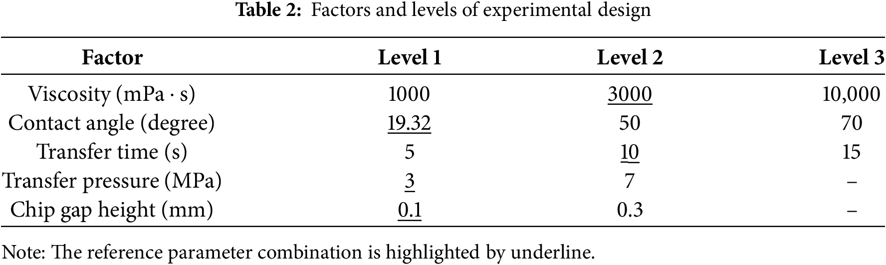
Viscosity represents material selection. The contact angle reflects process control. In general, plasma activation is performed prior to molding. This process results in a lower contact angle. However, the contact angle increases when the queue time of the semi-manufactured product between the plasma activation and molding processes is prolonged. The transfer time and pressure are process parameters controlled by the process engineer, whereas the chip gap height is a product design factor that is beyond the control of the process engineer.
To further assess the impact of key factors on void formation, sensitivity analyses were conducted as part of the design of experiments (DOE). The variations in viscosity, contact angle, transfer time, transfer pressure, and chip gap height were examined at different levels, and their effects on void size were systematically quantified. This approach enabled us to evaluate the relative importance of each factor and gain a deeper understanding of how these parameters influence the encapsulation process. The results of these sensitivity analyses provide valuable insights for optimizing the molding process and minimizing void formation in practical applications. Two or three levels were selected for each factor, as listed in Table 2. The one-factor-at-a-time method was selected for the experimental design. The reference parameter combination consists of 3000 mPa · s for the viscosity, 19.32 degrees for the contact angle, 10 s for the transfer time, 3 MPa for the transfer pressure, and 0.1 mm for the chip gap height, which are highlighted by underlining in Table 2. The range of each factor was determined based on practical experience and process knowledge. Specifically, level 1 of the contact angle (19.32°) corresponds to the condition used in our validation experiment, which simulates the surface of a flip-chip substrate immediately after plasma activation. Levels 2 (50°) and 3 (70°) represent typical values observed when the substrate has been left in queue for varying durations prior to molding. These values are consistent with real-world process variations and thus are representative of EMC-substrate interactions in practical flip-chip packaging scenarios.
The capillary force is influenced by the surface tension of the fluid and the contact angle between the fluid and the contact surfaces. Capillary effects are typically observed in small-scale systems. The comparison results regarding the effect of the capillary force are illustrated in Fig. 6. Fig. 6a shows the simulation results without considering the capillary force; Fig. 6b shows the simulation results including the capillary force, and Fig. 6c displays the experimental results.

Figure 6: Modeling validation by air pocket size: (a) simulation result without consideration of capillary force; (b) simulation result with consideration of capillary force; (c) experiment result
When the capillary force was not considered, the fluid was driven solely by the transfer pressure. In the thin gap (under the chip), the flow resistance owing to viscosity becomes dominant, making it difficult for the transfer pressure to drive the fluid forward. This explains why the simulation results without the capillary force exhibited larger air pockets than the experimental results.
Conversely, the simulation results those accounts for the capillary force shows smaller air pockets compared to the result without the capillary force. This is due to the additional driving force provided by capillary action. These results highlight the necessity of considering the capillary force in the mold flow simulation of the MUF process. In addition to the qualitative agreement between simulation results (Fig. 6b) and experimental observations (Fig. 6c), root mean square error (RMSE) and error percentage were employed to objectively evaluate the level of agreement. The RMSE was calculated to be 0.224, and the error percentage was 12.8%, using the experimental void volume as the reference.
Generally, the capillary number (
where the viscosity (

Figure 7: (a) The cross-section location and (b) the cross-section figure of the fluid velocity during the filling process of MUF
Fig. 7b shows that the velocity in the chip gap is 0.481 mm/s, which is significantly smaller than the velocity outside the chip (14.091 mm/s). Therefore, the capillary number was calculated as follows:
• At the chip gap:
• Outside the chip:
Wolf et al. [54] indicated that the capillary number for a capillary-dominated flow between parallel plates is typically in the range of
3.2 Void Size Reduction by Numerical Simulation
Based on the validated simulation model, an experimental design was developed to evaluate the influence of the design factors. Fig. 8 shows the flow-front positions for fluids with different viscosities, with all other material parameters kept constant, as listed in Table 1. The blue (smaller) circles indicate the flow fronts around the chips for fluids with varying viscosities. The positions of the flow fronts remain the same and are unaffected by the fluid viscosity. This is because the flow is governed primarily by the transfer speed rather than the transfer pressure. The same fluid volume must fill the mold cavity regardless of the viscosity; thus, the flow-front positions are identical at the same time.

Figure 8: Flow front for different viscosities of fluids: (a) 1000 mPa · s; (b) 3000 mPa · s; (c) 10,000 mPa · s
However, when focusing on the red (larger) circles in Fig. 8, it is evident that the positions of the flow fronts differ. The lower the viscosity, the greater the extension of the flow-front. This is because the capillary force is independent of the viscosity, and a fluid with lower viscosity resistance is more easily drawn by the same capillary force. These results demonstrate that the capillary force is significant in the gap under the chip and insignificant on the side of the chip. Therefore, it can be concluded that mold flow simulations for general transfer molding do not need to account for capillary force, whereas mold flow simulations for MUF must.
The overall numerical modeling results for the experimental design are summarized in Fig. 9, which was obtained using the one-factor-at-a-time method. A black horizontal line in Fig. 9 indicates the void size corresponding to the reference parameter combination, which is 2.05 mm3. A table was added to Fig. 9 to present the range and ranking of all studied factors. The range for each factor was calculated as the difference between the maximum and minimum void sizes resulting from its variation. Based on this data, the optimization potential is comparable to the reference void size, highlighting the significance of parameter tuning. The most influential factors are viscosity, chip gap height, transfer time, contact angle, and transfer pressure, in that order. The optimal combination includes lower viscosity, a larger chip gap height, longer transfer time, lower contact angle, and higher transfer pressure. This result underscores the critical role of product design. Although miniaturization trends may exacerbate the void issue, improvements can still be achieved through careful EMC material selection and process control. Further discussion on the influence of each factor and future prospects is provided in the following section.

Figure 9: Numerical modeling results for the experimental design; the reference void is the center air pocket. Note: The black horizontal line in the figure highlights the void size with the reference parameter combination
Furthermore, the viscosity of the working fluid was crucial. Selecting the EMC with the lowest viscosity during the filling phase is vital. However, the viscosity of the EMC changes owing to rising temperatures and the reactivity of the material. Thus, viscosity is influenced not only by the EMC’s intrinsic properties but also by the process temperature and time, which are factors within a process engineer’s control.
Regarding the contact angle, the results indicated that smaller angles were better. However, the difference in performance between 19.32° and 50° was much smaller than that between 50° and 70°. This suggests that there is no need for excessively stringent standards requiring contact angles to be significantly less than 50°.
The results also showed that a longer transfer time was beneficial but only if the viscosity remained constant. For EMC, the viscosity increases if the transfer time is too long. This is an important consideration for process designers. Therefore, there is an optimal transfer time for materials with reactive viscosities, such as EMC. This represents the maximum allowable time before the EMC viscosity begins to increase dramatically owing to the chemical reactions.
In summary, with the trend of miniaturization, several approaches can be considered to address the void issue. These include selecting an EMC with a lower initial viscosity and longer low-viscosity duration, extending the transfer time, and managing the queue time between plasma activation and molding to maintain the contact angle at or below 50°. Low viscosity during the flow process, or an extended low-viscosity window, can be achieved through both material selection and process condition optimization. From the perspective of material selection, a lower initial viscosity may be obtained by using low molecular weight resins or adjusting the filler content. A longer low-viscosity duration can be achieved by choosing lower-reactivity curing agents, reducing catalyst concentration, or incorporating rheology modifiers. From the perspective of process adjustments, reducing the mold temperature (e.g., from the typical 175°C to 165°C or 160°C) can decelerate the curing reaction and prolong the low-viscosity phase.
Real EMC materials exhibit temperature-dependent viscosity variations during the molding process. In this study, a constant-viscosity silicone oil was deliberately selected as a simplified substitute for EMC in the validation experiment. This choice enabled controlled and repeatable testing conditions, allowing us to focus on the quantitative investigation of flow behavior and void formation mechanisms without the added complexity of thermal effects. By introducing this simplification, the study was able to effectively capture the key flow mechanisms of the MUF process under controlled conditions. We recognize that assuming constant viscosity may limit the quantitative accuracy of void predictions for real EMCs. Nonetheless, the insights gained from this simplified model offer a valuable foundation for understanding flow behavior, which can inform more detailed, material-specific simulations in future work.
To evaluate void formation in MUF processes, this study designed a simplified mimic process involving a fluid visualization experiment using silicone oil as a substitute for EMC, and employed a numerical model assuming constant viscosity. These simplifications allowed controlled observations and analysis of flow behavior but may limit the quantitative accuracy of void prediction in actual EMC processes. The following conclusions can be drawn from the results of this study:
(a) This study successfully developed a fluid visualization experiment to evaluate the void formation in the chip gap during the MUF process of semiconductor packaging. The flow fronts and air pockets were observed during the experiment.
(b) These findings highlight the necessity of considering the capillary force when evaluating the voids in the chip gap during the MUF process using a mold flow simulation.
(c) The importance of design factors for the MUF process was evaluated, and their rankings were as follows: viscosity, chip gap height, transfer time, contact angle, and transfer pressure. The optimal combination consisted of lower viscosity, a larger chip gap height, longer transfer time, lower contact angle, and larger transfer pressure.
(d) This study emphasizes that the issue of void formation under the chip gap becomes more pronounced as MUF products move toward miniaturization, resulting in a lower chip gap.
(e) Detailed suggestions for the MUF process design are provided. It is essential to select the EMC with the lowest viscosity during the filling phase. The optimal transfer time corresponds to the maximum time before the EMC viscosity begins to increase significantly because of the chemical reaction.
(f) Different EMC formulations can significantly influence flow behavior and void formation. This study suggests selecting EMCs with low molecular weight resins or optimized filler content to reduce initial viscosity, and using lower-reactivity curing agents, reduced catalyst concentrations, or rheology modifiers to prolong the low-viscosity duration. Future work could include testing various EMC formulations to validate these suggestions.
(g) Therefore, smaller contact angles are preferable. However, when the contact angle is less than 50°, the improvement is negligible. This result provides a clear guideline for defining the contact angle criterion prior to molding.
Acknowledgement: The authors would like to thank the members of the R&D team and the technical support team of CoreTech System Co., Ltd., for their assistance with the mold flow analysis.
Funding Statement: The authors received no specific funding for this study.
Author Contributions: The authors confirm their contributions to the paper as follows: study conception and design: Ian Hu; data collection: Tzu-Chun Hung and Mu-Heng Zhou; analysis and interpretation of results: Ian Hu, Tzu-Chun Hung, and Mu-Heng Zhou; validation and investigation: Heng-Sheng Lin and Dao-Long Chen; draft manuscript preparation: Ian Hu. All authors reviewed the results and approved the final version of the manuscript.
Availability of Data and Materials: All data generated or analyzed during this study are included in this published article.
Ethics Approval: Not applicable.
Conflicts of Interest: The authors declare no conflicts of interest to report regarding the present study.
Nomenclature
| Capillary number | |
| Vector of the capillary force | |
| Entropy of the fluid | |
| Thermal conductivity of the fluid | |
| Pressure of the fluid | |
| Time | |
| Temperature of the fluid | |
| Velocity of the fluid | |
| Velocity vector of the fluid | |
| Volume fraction of the fluid at the flow front | |
| Curvature at the flow front | |
| Density of the fluid | |
| Viscosity of the fluid | |
| Shear stress tensor of the fluid | |
| Surface tension of the fluid | |
| Abbreviations | |
| 2D | Two dimensional |
| 3D | Three dimensional |
| CTE | Coefficient of thermal expansion |
| CUF | Capillary underfill |
| EMC | Epoxy molding compound |
| eMUF | Exposed-die molded underfill |
| IBM | International Business Machines Corporation |
| IC | Integrated circuit |
| MUF | Molded underfill |
| RMSE | Root mean square error |
| SiP | System-in-Package |
References
1. Caroline BH. Trends in IC packaging. In: 2009 European Microelectronics and Packaging Conference; 2009 Jun 15–18; Rimini, Italy. [Google Scholar]
2. Lau JH. Advanced packaging trends. In: Lau JH, editors. Semiconductor advanced packaging. Singapore: Springer; 2021. p. 465–89. doi: 10.1007/978-981-16-1376-0_11. [Google Scholar] [CrossRef]
3. Liu J, Li P, Zhoa J, Yu S. High-temperature polymer-based dielectrics for advanced electronic packaging. In: Zha JW, Dang ZM, editors. High temperature polymer dielectrics: fundamentals and applications in power equipment. Hoboken, NJ, USA: John Wiley & Sons, Inc.; 2023. p. 149–80. doi: 10.1002/9783527841059.ch5. [Google Scholar] [CrossRef]
4. Yu G, Shi H, Wang H. Integrated circuit package types. In: Wang Y, Chi MH, Lou JJC, Chen CZ, editors. Handbook of integrated circuit industry. Singapore: Springer; 2023. p. 1027–67. doi: 10.1007/978-981-99-2836-1_55. [Google Scholar] [CrossRef]
5. Lau JH. Recent advances and trends in advanced packaging. IEEE Trans Compon Packag Manuf Technol. 2022;12(2):228–52. doi:10.1109/TCPMT.2022.3144461. [Google Scholar] [CrossRef]
6. Becker KF, Joklitschke D, Braun T, Koch M, Thomas T, Schreier-Alt T, et al. Transfer molding technology for smart power electronics modules: materials and processes. J Microelectron Electron Packag. 2012;9(2):78–86. doi:10.4071/imaps.320. [Google Scholar] [CrossRef]
7. Phansalkar SP, Kim C, Han B. Effect of critical properties of epoxy molding compound on warpage prediction: a critical review. Microelectron Reliab. 2022;130:114480. doi:10.1016/j.microrel.2022.114480. [Google Scholar] [CrossRef]
8. Tamil J, Ore SH, Gan KY, Bo YY, Ng G, Wah PT, et al. Molding flow modeling and experimental study on void control for flip chip package panel molding with molded underfill technology. Int Symp Microelectron. 2011;2011(1):673–82. doi:10.4071/isom-2011-wp1-paper4. [Google Scholar] [CrossRef]
9. Nguyen L, Quentin C, Fine P, Cobb B, Bayyuk S, Yang H, et al. Underfill of flip chip on laminates: simulation and validation. IEEE Trans Compon Packag Technol. 1999;22(2):168–76. doi:10.1109/6144.774725. [Google Scholar] [CrossRef]
10. Wang T, Chew TH, Chew YX, Foo L. Reliability studies of flip chip package with reflowable underfill. In: Proceedings of the Pan Pacific Microelectronic Symposium; 2011 Jan 18–20; Kamuela, HI, USA. p. 65–70. [Google Scholar]
11. Zhang Z, Wong CP. Assembly of lead-free bumped flip-chip with no-flow underfills. IEEE Trans Electron Packag Manuf. 2002;25(2):113–9. doi:10.1109/TEPM.2002.1021636. [Google Scholar] [CrossRef]
12. Davis EM, Harding WE, Schwartz RS, Corning JJ. Solid logic technology: versatile, high-performance microelectronics. IBM J Res Dev. 1964;8(2):102–14. doi:10.1147/rd.441.0056. [Google Scholar] [CrossRef]
13. Tu KN, Zeng K. Tin-lead (SnPb) solder reaction in flip chip technology. Mater Sci Eng R Rep. 2001;34(1):1–58. doi:10.1016/S0927-796X(01)00029-8. [Google Scholar] [CrossRef]
14. Wu JD, Zheng PJ, Lee CW, Hung SC, Lee JJ. A study in flip-chip UBM/bump reliability with effects of SnPb solder composition. In: 2003 IEEE International Reliability Physics Symposium Proceedings; 2003 Mar 30–Apr 4; Dallas, TX, USA. p. 132–9. doi:10.1109/RELPHY.2003.1197733. [Google Scholar] [CrossRef]
15. Oppermann H. The role of Au/Sn solder in packaging. In: Zschech E, Whelan C, Mikolajick T, editors. Materials for information technology: devices, interconnects packaging. London, UK: Springer; 2005. p. 377–90. doi: 10.1007/1-84628-235-7. [Google Scholar] [CrossRef]
16. Datta M. Manufacturing processes for fabrication of flip-chip micro-bumps used in microelectronic packaging: an overview. J Micromanuf. 2020;3(1):69–83. doi:10.1177/2516598419880124. [Google Scholar] [CrossRef]
17. Ng FC, Abas MA. Underfill flow in flip-chip encapsulation process: a review. J Electron Packag. 2022;144(1):010803. doi:10.1115/1.4050697. [Google Scholar] [CrossRef]
18. Depiver JA, Mallik S, Harmanto D. Solder joint failures under thermo-mechanical loading conditions—a review. Adv Mater Process Technol. 2021;7(1):1–26. doi:10.1080/2374068x.2020.1751514. [Google Scholar] [CrossRef]
19. Wang B, Li W, Zhang S, Li X, Pan K. Effect of electric current stressing on mechanical performance of solders and solder joints: a review. J Mater Sci. 2022;57(37):17533–62. doi:10.1007/s10853-022-07715-6. [Google Scholar] [CrossRef]
20. Jian M, Hamasha S, Alahmer A, Wei X, Belhadi MA, Alakayleh A, et al. Shear fatigue analysis of SAC-Bi solder joint exposed to varying stress cycling conditions. IEEE Trans Compon Packag Manuf Technol. 2023;13(2):274–83. doi:10.1109/TCPMT.2023.3240367. [Google Scholar] [CrossRef]
21. Waseem A, Ibrahim MS, Lu C, Waseem M, Lee HH, Loo KH. The effect of pre-existing voids on solder reliability at different thermomechanical stress levels: experimental assessment. Mater Des. 2023;233(8):112275. doi:10.1016/j.matdes.2023.112275. [Google Scholar] [CrossRef]
22. Park SY, On SY, Kim J, Lee J, Kim T-S, Wardle BL, Kim SS. Electronic packaging enhancement engineered by reducing the bonding temperature via modified cure cycles. ACS Appl Mater Interfaces. 2023;15(8):11024–32. doi:10.1021/acsami.2c21229. [Google Scholar] [PubMed] [CrossRef]
23. Salahouelhadj A, Gonzalez M, Vanstreels K, van der Plas G, Beyer G, Beyne E. Analysis of warpage of a flip-chip BGA package under thermal loading: finite element modelling and experimental validation. Microelectron Eng. 2023;271(3):111947. doi:10.1016/j.mee.2023.111947. [Google Scholar] [CrossRef]
24. Gan CL, Chung MH, Lin LF, Huang CY, Takiar H. Evolution of epoxy molding compounds and future carbon materials for thermal and mechanical stress management in memory device packaging: a critical review. J Mater Sci Mater Electron. 2023;34(30):2011. doi:10.1007/s10854-023-11388-5. [Google Scholar] [CrossRef]
25. Hu I, Huang YR, Lin HS, Chen DL. Effect of effective curing shrinkage of EMC on strip warpage during IC encapsulation process. IEEE Trans Compon Packag Manuf Technol. 2024;14(11):2088–97. doi:10.1109/TCPMT.2024.3488009. [Google Scholar] [CrossRef]
26. Liang SW, Wu GCY, Yee KC, Wang CT, Cui JJ, Yu DCH. High performance and energy efficient computing with advanced SoICTM scaling. In: 2022 IEEE 72nd Electronic Components and Technology Conference (ECTC); 2022 May 31–Jun 3; San Diego, CA, USA. doi: 10.1109/ECTC51906.2022.00176. [Google Scholar] [CrossRef]
27. Li Z, Luo H, Jiang Y, Liu H, Xu L, Cao K, et al. Comprehensive review and future prospects on chip-scale thermal management: core of data center’s thermal management. Appl Therm Eng. 2024;251:123612. doi:10.1016/j.applthermaleng.2024.123612. [Google Scholar] [CrossRef]
28. Wang C, Qiu M, Pan Z, Zhou K, Wang T, Hong J, et al. Optimized design of contact interfaces for enhanced heat dissipation in flip-chip package. Appl Therm Eng. 2025;259:124936. doi:10.1016/j.applthermaleng.2024.124936. [Google Scholar] [CrossRef]
29. Hu I, Kuo YC, Yang TS. High-efficiency extraction method for thermal network model of advanced electronic packages. IEEE Trans Compon Packag Manuf Technol. 2025;15(4):716–24. doi:10.1109/TCPMT.2025.3547229. [Google Scholar] [CrossRef]
30. Ng FC, Abas A, Nashrudin MN, Tura Ali MY. Analytical and numerical analyses of filling progression and void formation in flip-chip underfill encapsulation process. Solder Surf Mo Technol. 2022;34(4):193–202. doi:10.1108/ssmt-08-2021-0055. [Google Scholar] [CrossRef]
31. Ling C, Azahari MT, Abas MA, Ng FC. Deep learning and analytical study of void regional formation in flip-chip underfilling process. Solder Surf Mo Technol. 2024;36(1):60–8. doi:10.1108/ssmt-06-2023-0028. [Google Scholar] [CrossRef]
32. Ling C, Azahari MT, Abas MA, Ng FC. Correlation study on voiding in underfill of large quantity ball grid array chip using machine learning. J Electron Packag. 2025;147(1):011001. doi:10.1115/1.4065077. [Google Scholar] [CrossRef]
33. Huang BY, Hu I, Chen JDL, Tarng D, Hung CP. Design for void free transfer molding SiP. In: 2020 15th International Microsystems, Packaging, Assembly and Circuits Technology Conference (IMPACT); 2020 Oct 21–23; Taipei, Taiwan. p. 40–4. doi:10.1109/impact50485.2020.9268552. [Google Scholar] [CrossRef]
34. Lin Y, Hu I, Chen DL, Tarng D, Hung CP. Compression molding mechanism and parameter evaluation of SiP. In: 2020 15th International Microsystems, Packaging, Assembly and Circuits Technology Conference (IMPACT); 2020 Oct 21–23; Taipei, Taiwan. p. 116–20. doi:10.1109/impact50485.2020.9268556. [Google Scholar] [CrossRef]
35. Hung HH, Cheng YC, Hwang SJ, Chen DL, Chang HJ, Huang BY, et al. Analysis of flip-chip ball grid array underfill flow process. Int J Adv Manuf Technol. 2024;134(9):4851–70. doi:10.1007/s00170-024-14304-1. [Google Scholar] [CrossRef]
36. Hung HH, Cheng YC, Hwang SJ, Chang HJ, Huang BY, Huang HH, et al. Effect of flip-chip ball grid array structure on capillary underfill flow. Results Eng. 2024;23(1):102527. doi:10.1016/j.rineng.2024.102527. [Google Scholar] [CrossRef]
37. Chen KM. Comparing the impacts of the capillary and the molded underfill process on the reliability of the flip-chip BGA. IEEE Trans Compon Packag Technol. 2008;31(3):586–91. doi:10.1109/TCAPT.2008.2001161. [Google Scholar] [CrossRef]
38. Hu I. Mechanics modeling of eMUF FC BGA molding process for bump deformation control. In: 2015 10th International Microsystems, Packaging, Assembly and Circuits Technology Conference (IMPACT); 2015 Oct 21–23; Taipei, Taiwan. p. 285–7. doi:10.1109/IMPACT.2015.7365217. [Google Scholar] [CrossRef]
39. Chang RY, Yang WH, Hwang SJ, Su F. Three-dimensional modeling of mold filling in microelectronics encapsulation process. IEEE Trans Compon Packag Technol. 2004;27(1):200–9. doi:10.1109/TCAPT.2003.821682. [Google Scholar] [CrossRef]
40. Lee MW, Jung WK, Sohn ES, Lee JY, Hwang CH, Lee CH. A study on the rheological characterization and flow modeling of molded underfill (MUF) for optimized void elimination design. In: 2008 58th Electronic Components and Technology Conference; 2008 May 27–30; Lake Buena Vista, FL, USA. p. 382–8. doi:10.1109/ECTC.2008.4550000. [Google Scholar] [CrossRef]
41. Chen BH, Hwang SJ, Chang YY, Yang YS, Lee HH, Huang BY, et al. Epoxy molding compound filler clogging simulation during integrated circuit encapsulation process. IEEE Trans Compon Packag Manuf Technol. 2022;12(1):174–84. doi:10.1109/TCPMT.2021.3129886. [Google Scholar] [CrossRef]
42. Chen YK, Wu GT, Hwang SJ, Lee HH, Hwang DY. Molded underfill for flip chip package. In: 2013 8th International Microsystems, Packaging, Assembly and Circuits Technology Conference (IMPACT); 2013 Oct 22–25; Taipei, Taiwan. p. 310–4. doi:10.1109/IMPACT.2013.6706663. [Google Scholar] [CrossRef]
43. Choi KW, Baick IH, Lee D, Lee E, Kwon E, Pae S, et al. Two-phase flow simulation of molded underfill process to mitigate void and assure reliability at product level. In: 2016 IEEE 66th Electronic Components and Technology Conference (ECTC); 2016 May 31–Jun 3; Las Vegas, NV, USA. p. 660–5. doi:10.1109/ECTC.2016.34. [Google Scholar] [CrossRef]
44. Wu KT, Hwang SJ, Lee HH. Mechanism of void prediction in flip chip packages with molded underfill. J Electron Mater. 2017;46(8):5094–106. doi:10.1007/s11664-017-5516-7. [Google Scholar] [CrossRef]
45. Hsu CC, Huang CT, Chang RY. Void risk prediction for semiconductor packages considering the air venting analysis with fluid/structure interaction method. In: 2016 IEEE 18th Electronics Packaging Technology Conference (EPTC); 2016 Nov 30–Dec 3; Singapore. p. 185–9. doi:10.1109/EPTC.2016.7861468. [Google Scholar] [CrossRef]
46. Merzkirch W. Flow visualization. Cambridge, MA, USA: Academic Press; 1987. [Google Scholar]
47. Smits AJ, Lim TT. Flow visualization: techniques and examples. London, UK: Imperial College Press; 2012. [Google Scholar]
48. Su CH, Chen CC, Hung YC, Ting CC. Optical flow visualization using the modular back-ground-oriented full-scale schlieren technique. Int J Eng Technol Innov. 2014;4(3):182–93. [Google Scholar]
49. Ryu JD, Ha KN, Lee DG, Nam KS. Flow analysis of underwater water jet system using computational fluid dynamics and particle image velocimetry. Proc Eng Technol Innov. 2017;6:23–7. [Google Scholar]
50. Guo XR, Young WB. A two-dimensional simulation model for the molded underfill process in flip chip packaging. J Mech Sci Technol. 2015;29(7):2967–74. doi:10.1007/s12206-015-0627-7. [Google Scholar] [CrossRef]
51. Guo XR, Young WB. Vacuum effect on the void formation of the molded underfill process in flip chip packaging. Microelectron Reliab. 2015;55(3–4):613–22. doi:10.1016/j.microrel.2014.12.001. [Google Scholar] [CrossRef]
52. Chen SL, Dinh HN, Nguyen VT. Synchronized injection molding machine with servomo-tors. Adv Technol Innov. 2017;2(2):34–9. [Google Scholar]
53. Abbott JR, Higgins BG. Surface tension of a curing epoxy. J Polym Sci Part A Polym Chem. 1988;26(7):1985–8. doi:10.1002/pola.1988.080260724. [Google Scholar] [CrossRef]
54. Wolf FG, dos Santos LO, Philippi PC. Capillary rise between parallel plates under dynamic conditions. J Colloid Interface Sci. 2010;344(1):171–9. doi:10.1016/j.jcis.2009.12.023. [Google Scholar] [PubMed] [CrossRef]
Cite This Article
 Copyright © 2025 The Author(s). Published by Tech Science Press.
This work is licensed under a Creative Commons Attribution 4.0 International License , which permits unrestricted use, distribution, and reproduction in any medium, provided the original work is properly cited.
 Downloads
 Citation Tools