
 Submit a Paper
 Propose a Special lssue
 Open Access
ARTICLE

Lightweight Small Defect Detection with YOLOv8 Using Cascaded Multi-Receptive Fields and Enhanced Detection Heads
Department of Information and Communication Engineering, Beijing Information Science and Technology University, Beijing, 102206, China
* Corresponding Author: Zhensong Li. Email:
Computers, Materials & Continua 2026, 86(1), 1-14. https://doi.org/10.32604/cmc.2025.068138
Received 21 May 2025; Accepted 27 August 2025; Issue published 10 November 2025
 View Full Text
 Download PDF
Abstract
In printed circuit board (PCB) manufacturing, surface defects can significantly affect product quality. To address the performance degradation, high false detection rates, and missed detections caused by complex backgrounds in current intelligent inspection algorithms, this paper proposes CG-YOLOv8, a lightweight and improved model based on YOLOv8n for PCB surface defect detection. The proposed method optimizes the network architecture and compresses parameters to reduce model complexity while maintaining high detection accuracy, thereby enhancing the capability of identifying diverse defects under complex conditions. Specifically, a cascaded multi-receptive field (CMRF) module is adopted to replace the SPPF module in the backbone to improve feature perception, and an inverted residual mobile block (IRMB) is integrated into the C2f module to further enhance performance. Additionally, conventional convolution layers are replaced with GSConv to reduce computational cost, and a lightweight Convolutional Block Attention Module based Convolution (CBAMConv) module is introduced after Grouped Spatial Convolution (GSConv) to preserve accuracy through attention mechanisms. The detection head is also optimized by removing medium and large-scale detection layers, thereby enhancing the model’s ability to detect small-scale defects and further reducing complexity. Experimental results show that, compared to the original YOLOv8n, the proposed CG-YOLOv8 reduces parameter count by 53.9, improves mAP@0.5 by 2.2, and increases precision and recall by 2.0 and 1.8, respectively. These improvements demonstrate that CG-YOLOv8 offers an efficient and lightweight solution for PCB surface defect detection.Keywords
Printed Circuit Board (PCB) surface defect detection is essential for guaranteeing both product reliability and production stability in modern electronics. As industrial automation has advanced, Automated Optical Inspection (AOI) has gradually become the dominant approach for PCB defect detection [1]. However, conventional AOI systems are often limited by high false alarm rates and insufficient efficiency, especially when confronted with complicated defect patterns. These shortcomings make it difficult to fully satisfy the industry’s demand for precise and efficient quality control.
In recent years, deep learning has advanced rapidly in computer vision and has increasingly been applied to PCB defect inspection, driving the progress of intelligent quality control systems [2]. Detection algorithms based on deep learning are generally grouped into two main categories: two-stage and one-stage frameworks [3]. Two-stage methods, such as Faster R-CNN and Cascade R-CNN [4], generate candidate regions before performing classification and localization, which leads to high accuracy but also adds computational burden. By contrast, one-stage approaches like SSD and the YOLO family [5] perform prediction in a single step, offering much faster inference and making them well suited for real-time use. With the ongoing push toward lightweight models, one-stage detectors have shown clear advantages in PCB-related applications and are often favored in industrial settings [6]. Among these, the YOLO series has become especially popular for its balance between speed and precision. In particular, YOLOv8 provides a practical trade-off between accuracy and inference efficiency, making it a strong candidate for PCB surface defect detection [7–9].
Despite these advances, two major difficulties remain: defects are usually very small in scale, and computing resources are often limited in practice. To mitigate these problems, researchers have placed more emphasis on compact network designs and optimization strategies. Typical approaches—such as pruning, quantization, and attention mechanisms—have been shown to maintain reliable accuracy while reducing computational load [10–13]. These improvements allow real-time deployment on hardware platforms with restricted resources, such as embedded and edge devices, which is especially important in industrial environments that require accuracy under strict time constraints [14].
In this work, the choice of key modules is guided by their proven effectiveness in balancing detection accuracy and computational efficiency. Specifically, the Cascade Multi-Receptive Field (CMRF) module replaces the conventional the conventional Spatial Pyramid Pooling-Fast (SPPF) to enhance multi-scale feature representation, which is critical for capturing tiny and diverse PCB defects. The Inverted Residual Mobile Block (IRMB), inspired by the lightweight MobileNetV2 bottleneck structure, is integrated into the C2f module to improve feature extraction while maintaining low complexity. Grouped Spatial Convolution (GSConv), combining group and pointwise convolutions, is adopted to significantly reduce parameter count and FLOPs without major accuracy loss. To counteract the information loss caused by lightweight convolutions, a Convolutional Block Attention Module based Convolution (CBAMConv) module is inserted, leveraging channel and spatial attention mechanisms to enhance the model’s focus on relevant defect features. These design decisions enable the proposed CG-YOLOv8 to achieve high detection performance on tiny PCB defects with reduced computational cost, facilitating deployment on resource-constrained platforms.
Liao et al. proposed YOLOv4-MN3, replacing the backbone with MobileNetV3 and introducing PANet and the Mish activation function. However, the redundant modules resulted in high computational complexity, hindering real-time deployment [15]. For one-stage models, Du et al. proposed YOLO MBBi, integrating MBConv, CBAM, and BiFPN modules to boost small object detection and reduce parameter count, though ultra-small defects remained challenging [16]. Peng et al. introduced YOLO RRL, incorporating RFD, RepGFPN, DySample, and LADH Head modules, achieving a 2.2
Fig. 1 presents typical examples of PCB images before and after defect detection. The raw PCB surface (a) contains subtle defects that are difficult to identify using traditional methods. The detection result (b) clearly highlights the defect regions, demonstrating the effectiveness of automated inspection techniques in revealing tiny and complex defects. This visual comparison underscores the necessity of developing efficient and accurate PCB defect detection algorithms.
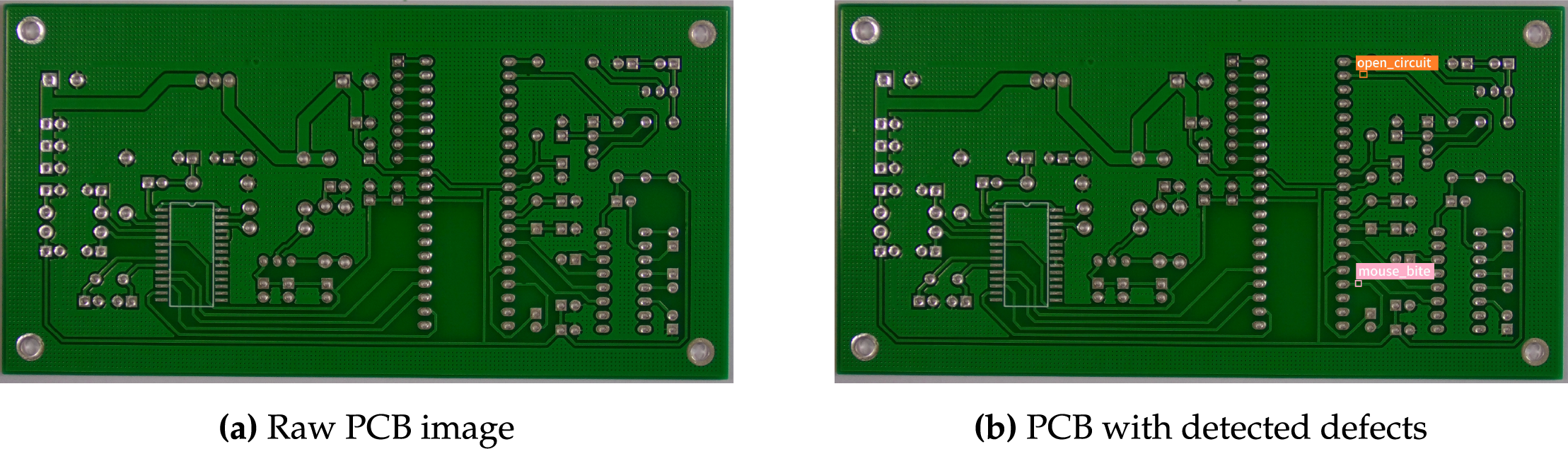
Figure 1: Typical PCB images illustrating defect presence and detection results
Considering the challenges introduced by complex backgrounds and the variety of defect types in PCB inspection, this study develops CG-YOLOv8, a lightweight model derived from YOLOv8n. The proposed framework refines the network design and minimizes redundant parameters while maintaining high detection precision. As a result, it achieves better recognition of very small defects in complicated scenarios with lower computational cost.
In this study, we put forward four specific improvements to strengthen PCB defect detection:
1. We replace the traditional SPPF block with a Cascade Multi-Receptive Field (CMRF) module, which enhances the model’s ability to capture features at different scales and makes it more robust in complex backgrounds.
2. An Inverted Residual Mobile Block (IRMB) is added into the C2f module. This enriches the feature extraction path and helps the network learn subtle defect patterns, while still keeping the model lightweight.
3. To further reduce computation, standard convolutions are swapped for GSConv. To avoid accuracy loss caused by this lightweighting, we add CBAMConv, which directs the network’s attention toward key defect regions.
4. Finally, the medium and large detection heads are removed, leaving only the small-scale head. This makes the architecture simpler and improves the ability to detect tiny defects, which are most common in PCB inspection.
Built on the YOLOv8n model, CG-YOLOv8 targets fine-scale PCB defects; the overall architecture is shown in Fig. 2. We replace the original Spatial Pyramid Pooling Fast (SPPF) block with the proposed Cascade Multi-Receptive Field (CMRF) module to strengthen multi-scale feature cues. An Inverted Residual Mobile Block (IRMB) is inserted into the C2f path so the network can learn more intricate defect characteristics. To favor small targets, the medium- and large-scale detection heads are removed, which simplifies the network and concentrates capacity on the high-resolution branch. Standard convolution is also swapped for Grouped Spatial Convolution (GSConv) to shrink parameters and computation. Finally, a Convolutional Block Attention Module based Convolution (CBAMConv) is attached after GSConv to steer attention toward informative defect regions, preserving detection accuracy under a lower computational budget.
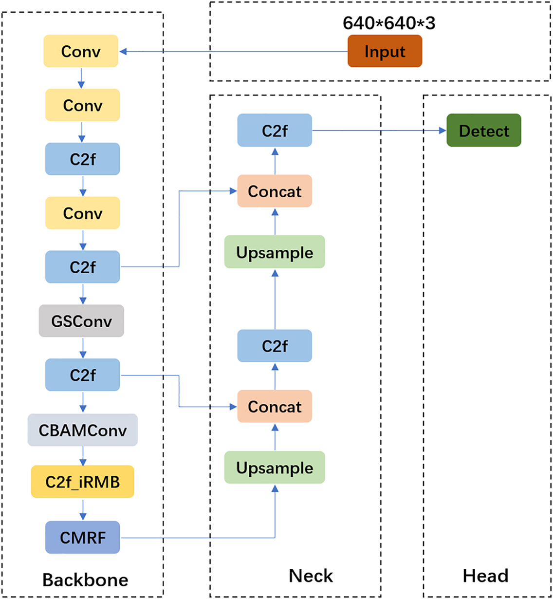
Figure 2: CG-YOLOv8n network structure
3.1 Backbone Network Optimization with CMRF and iRMB
In object detection and image recognition, the receptive field (RF) is a key factor influencing feature extraction. If the RF is too small, the model may fail to capture global semantic context; if it is too large, fine local details can be overlooked. To overcome the drawbacks of relying on a single-scale receptive field, the Cascade Multi-Receptive Field (CMRF) module is introduced. It aggregates information from multiple scales, ensuring that local detail is preserved while also capturing broad semantic cues [20].
The CMRF module generally stacks convolutional layers with different kernel sizes or dilation rates. This setup enables the network to process features at several receptive field scales while maintaining spatial resolution. By combining a multi-branch structure with feature fusion, the CMRF module emulates the human visual system in considering both overall structure and fine detail. This design improves the model’s capability to detect small targets, objects of varying scales, and features embedded in complex backgrounds.
As shown in Fig. 3, a typical CMRF block contains several parallel branches. One may use a 3
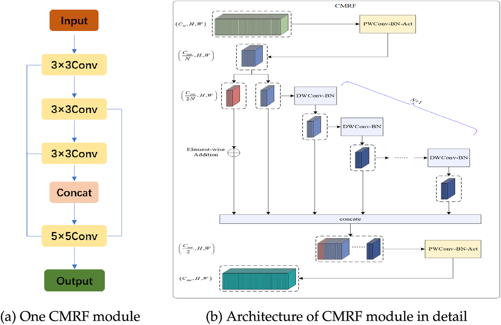
Figure 3: Overview of the proposed CMRF structure
Integrating CMRF strengthens the network’s ability to handle objects at different scales, which is especially beneficial for PCB surface defect detection and other small-object recognition tasks. In such applications, defects like micro-cracks or subtle short circuits are often tiny and irregular, making single-scale features insufficient. With its multi-scale fusion strategy, CMRF improves both accuracy and robustness [22]. Section 5.1 further demonstrates that replacing CMRF with other fusion methods reduces detection performance, verifying its effectiveness.
Among them, the Inverted Residual Block (IRB) was first introduced in MobileNetV2, where it helped cut down parameters and computational overheads [23]. Building on this concept, the Inverted Residual Mobile Block (IRMB) is inspired by the Meta Mobile Block (MMB), which provides a general framework for lightweight network construction. IRMB adopts a single-residual-branch structure that combines depth-wise separable convolutions with an enhanced window-based multi-head self-attention (EW-MHSA) mechanism. This combination allows the model to capture both local details and global dependencies while still keeping the architecture lightweight [24]. Instead of simply reducing parameters or directly boosting accuracy, IRMB delivers a compact and adaptable backbone that facilitates the integration of subsequent modules.
3.2 GSConv and CBAM for Efficient Feature Representation
To improve inference efficiency while keeping the model compact, this work adopts the GSConv structure. GSConv is a lightweight convolutional unit that reduces both parameter size and computational burden, yet still maintains sufficient representational power.
As shown in Fig. 4, GSConv integrates standard convolution with depth-wise separable convolution. The standard branch focuses on capturing spatial features, whereas the depth-wise branch lowers computation. Their outputs are concatenated and refined through Channel Shuffle, which facilitates more effective feature fusion. This design achieves a balance between efficiency and accuracy, providing competitive expressive ability at a reduced computational cost [25]. Owing to these advantages, GSConv is employed in our model to further lower complexity without compromising representational strength.

Figure 4: GSConv module
To strengthen feature representation, the Convolutional Block Attention Module (CBAM) is incorporated. In this study, CBAM is directly combined with a convolutional layer, referred to as CBAMConv, so that the attention mechanism is embedded into the convolution process. Originally proposed by Woo et al. at ECCV 2018, CBAM applies channel and spatial attention in sequence, adaptively highlighting informative features and suppressing redundant ones [26]. Prior research has confirmed CBAM’s effectiveness in enhancing feature learning with minimal extra computation, which motivates its adoption here to improve model accuracy while preserving efficiency. Specifically, CBAM recalibrates features through two complementary submodules. The Channel Attention Module assigns importance weights to each channel using global average pooling and max pooling, followed by a shared MLP and Sigmoid normalization. The Spatial Attention Module then generates a spatial attention map by applying channel-wise pooling and a 7
3.3 Detection Head Optimization
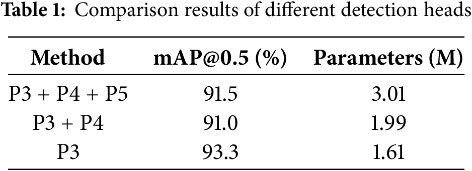
In the baseline YOLOv8n network, three detection heads are distributed across the 15th, 18th, and 21st layers, each designed to handle objects of different scales—small, medium, and large. This multi-head structure provides general versatility for a wide range of object detection tasks. However, in the case of PCB surface inspection, the situation is quite different: defects such as micro-cracks, burrs, or missing holes usually appear extremely small and occupy only a limited area of the board image. As a result, the contribution of the medium- and large-object detection heads becomes marginal, while still introducing additional computational burden.
To better adapt the model to the characteristics of PCB defect detection, the architecture of YOLOv8n was streamlined by discarding the medium- and large-scale detection heads and retaining only the high-resolution head. In doing so, the network concentrates its representational capacity on small targets, which directly aligns with the nature of PCB defects. This modification not only decreases the number of parameters and lowers computational cost, but also improves inference efficiency and reduces redundant feature extraction.
Ablation experiments further verify that focusing exclusively on the small-object detection head yields higher accuracy for defect categories dominated by fine structures, while significantly accelerating detection speed. This adjustment therefore enhances both the efficiency and practicality of the model for real-world industrial deployment scenarios where small defect detection is the primary concern.
The optimized version therefore keeps only the P3 head and discards the P4 and P5 heads along with their feature pyramids. This modification lowers model complexity and improves the recognition of small defects. Results from ablation experiments (see Table 1) confirm that using only the high-resolution head delivers the best performance for PCB defect detection. In addition, the simplified network operates faster, making it more suitable for industrial use. These observations suggest that the original three-head structure is less appropriate for defect detection tasks that are mainly concerned with small objects.
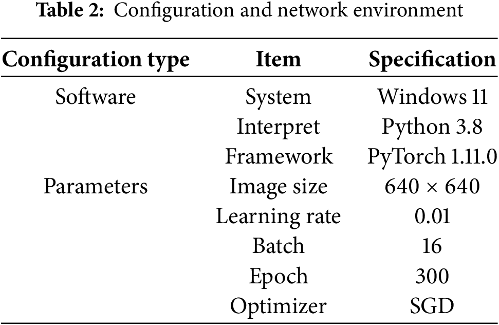
The experiments were performed on a workstation running Windows 11, equipped with an NVIDIA RTX 4090 GPU with 24 GB of memory. The implementation was based on the PyTorch 1.11.0 framework. During training, input images were resized to 640
For reproducibility, a fixed random seed was used (the default in Ultralytics YOLOv8 is 0), allowing the training process to be repeated under identical settings. Since training deep neural networks requires substantial time and computational resources, additional independent runs or cross-validation tests for statistical significance were not conducted. Even so, consistent improvements were obtained across multiple defect categories and evaluation metrics, suggesting that the proposed modifications are both reliable and robust. The model also displayed stable convergence throughout training, which provides further evidence of its effectiveness. In future work, more comprehensive statistical testing and repeated experiments could be carried out as hardware resources become available.
The dataset utilized in this research is the publicly available PCB dataset released by the Intelligent Robotics Open Laboratory at Peking University. It comprises a total of 693 high-resolution circuit board images, each with an average resolution of 2777
The dataset contains a total of 693 images, with the number of samples in each defect type kept close to one another, as shown in Table 3. Such a balanced distribution minimizes potential bias toward any specific category, which is particularly important for training lightweight detection models. To enable both model optimization and reliable performance evaluation, the dataset was divided into training and testing subsets in an 8:2 ratio. This allocation provides sufficient data for effective learning while reserving an independent portion for validation, thereby supporting fair assessment of the proposed method.

In evaluating object detection performance, three indicators are primarily considered: Precision (P), Recall (R), and mean Average Precision at IoU threshold 0.5 (mAP@0.5). Precision indicates how many of the predicted targets are actually correct, while Recall emphasizes how many real targets have been successfully retrieved by the model. Unlike these single indicators, mAP@0.5 provides a more comprehensive view by averaging the Average Precision (AP) values across all categories. The AP itself is obtained from the area under the Precision-Recall (P-R) curve, with values that vary continuously between 0 and 1.
For practical evaluation, the prediction outcomes can be classified into four groups: a True Positive (TP) when a real defect is correctly detected, a True Negative (TN) when a non-defect is accurately rejected, a False Positive (FP) when a non-defect is mistakenly predicted as defective, and a False Negative (FN) when an actual defect is missed. These criteria together offer a rigorous framework for measuring both the accuracy and completeness of the detection model.
To assess the effectiveness of the proposed CG-YOLOv8, an ablation study was carried out on the dataset under identical experimental conditions. The improvement modules were introduced step by step into the baseline YOLOv8n to measure their individual contributions. The corresponding results are reported in Table 4. As shown in Table 4, Model_1, which corresponds to the original YOLOv8n, achieved a mAP@0.5 of 91.5

In addition to detection accuracy and parameter scale, we also assessed inference speed (FPS) and computational complexity (GFLOPs) to better evaluate the deployment feasibility of different modules. As shown in Table 4, removing the P4 and P5 detection heads (Model_6) resulted in an increase in mAP@0.5 while reducing the computational burden, with FPS improving from 1.46 to 1.45 and GFLOPs decreasing from 8.1 to 6.0, indicating a lighter and more efficient model. The introduction of the CMRF and IRMB modules preserved relatively stable inference speed while further lowering parameter counts and GFLOPs. In contrast, GSConv (Model_9) produced a slight decline in accuracy but achieved notable reductions in both computational complexity and parameter size, reflecting a clear balance between efficiency and precision. Finally, the proposed CG-YOLOv8 (Model_10) demonstrated an overall improvement by increasing detection accuracy, maintaining competitive FPS, and substantially reducing computational cost, making it more practical for scenarios with restricted resources or for deployment on portable devices.
The outcomes in Table 4 further confirm that each individual modification has a positive impact on model performance. Compared with the baseline YOLOv8n, CG-YOLOv8 not only improves accuracy but also decreases both parameter overhead and computation demand, leading to faster inference and a more compact architecture. These characteristics render the model particularly advantageous for hardware-constrained environments, such as embedded platforms or mobile systems, highlighting its strong applicability in real-world industrial settings.
The effectiveness of CG-YOLOv8 was further validated by benchmarking it against several mainstream detectors. Under the same experimental settings, mAP@0.5 and parameter size were measured, with the outcomes summarized in Table 5. The baselines used for comparison were SSD, Faster R-CNN, YOLOv5s, YOLOv8n, and YOLOv10n. Experimental findings show that CG-YOLOv8 achieves superior accuracy and efficiency across all benchmarks, with mAP@0.5 improvements of 18.3

To evaluate the robustness of CG-YOLOv8n, we analyzed missed detection cases. Although the overall mAP@0.5 is high (Table 5), the model occasionally fails to detect subtle defects in low-contrast or complex backgrounds (Fig. 5). This highlights the need to refine feature extraction and incorporate attention mechanisms to improve detection sensitivity and generalization.

Figure 5: Missed detection case
In addition, Fig. 6 provides a side-by-side comparison of YOLOv8n and CG-YOLOv8 across six PCB defect categories. Relative to YOLOv8n, the proposed method reduces parameter count by 53.9

Figure 6: Detection effect on different models

Ten independent paired training runs were conducted for both the original YOLOv8n and the proposed CG-YOLOv8n models, with the mAP@0.5 results shown in Table 7. A paired

To evaluate the robustness of CG-YOLOv8n, we analyzed missed detection cases. Although the overall mAP@0.5 is high (Table 5), the model occasionally fails to detect subtle defects in low-contrast or complex backgrounds (Fig. 5). This highlights the need to refine feature extraction and incorporate attention mechanisms to improve detection sensitivity and generalization.
This work introduces CG-YOLOv8, a lightweight model for PCB defect detection that reduces structural complexity while maintaining competitive accuracy. Comprehensive experiments, including baseline comparisons and ablation studies, confirmed that CG-YOLOv8 achieves superior accuracy and efficiency while substantially reducing parameter overhead.
Despite these encouraging results, challenges remain in handling extremely small defects under complex backgrounds, which may compromise robustness in real-world scenarios. Future research will consider the integration of stronger attention mechanisms, compression techniques, and hardware-oriented optimizations for embedded platforms such as Jetson Nano. In addition, extending the framework with anomaly detection and semi-supervised training strategies, as well as testing across broader defect datasets, will help further enhance its generalization ability.
Moreover, the lightweight nature of CG-YOLOv8 makes it highly suitable for real-time deployment on production lines, where detection speed and stability are critical. Future work could also explore validating the model under more diverse manufacturing conditions, such as noisy environments and PCB datasets from different vendors, to further strengthen robustness and general applicability.
In summary, CG-YOLOv8 demonstrates the potential to deliver real-time PCB defect detection with a good balance between accuracy and efficiency, making it a practical candidate for deployment in modern manufacturing environments.
Acknowledgement: The authors thank all those who provided helpful guidance and constructive suggestions during this work.
Funding Statement: This research was funded by the Joint Funds of the National Natural Science Foundation of China (U2341223) and the Beijing Municipal Natural Science Foundation (No. 4232067).
Author Contributions: The authors confirm contribution to the paper as follows: Conceptualization, Shengran Zhao and Zhensong Li; Methodology, Shengran Zhao; Software, Shengran Zhao; Validation, Shengran Zhao, Xiaotan Wei, and Yutong Wang; Formal analysis, Shengran Zhao; Investigation, Shengran Zhao, Xiaotan Wei, and Yutong Wang; Resources, Kai Zhao; Data curation, Shengran Zhao and Zhensong Li; Writing—original draft preparation, Shengran Zhao; Writing—review and editing, Shengran Zhao and Zhensong Li; Visualization, Shengran Zhao; Supervision, Zhensong Li; Project administration, Zhensong Li; Funding acquisition, Zhensong Li. All authors reviewed the results and approved the final version of the manuscript.
Availability of Data and Materials: The data that support the findings of this study are openly available in the PKU-PCB dataset at http://robotics.pkusz.edu.cn/resources/dataset/ (accessed on 26 August 2025).
Ethics Approval: Not applicable.
Conflicts of Interest: The authors declare no conflicts of interest to report regarding the present study.
References
1. Calabrese M, Agnusdei L, Fontana G, Papadia G, Del Prete A. Application of mask R-CNN and YOLOv8 algorithms for defect detection in printed circuit board manufacturing. Discover Appl Sci. 2025;7(4):257. doi:10.1007/s42452-025-06641-x. [Google Scholar] [CrossRef]
2. Ameri R, Hsu C-C, Band SS. A systematic review of deep learning approaches for surface defect detection in industrial applications. Eng Appl Artif Intell. 2024;130(3):107717. doi:10.1016/j.engappai.2023.107717. [Google Scholar] [CrossRef]
3. Chen X, Wu Y, He X, Ming W. A comprehensive review of deep learning-based PCB defect detection. IEEE Access. 2023;11(6):139017–38. doi:10.1109/access.2023.3339561. [Google Scholar] [CrossRef]
4. Xia K, Lv Z, Liu K, Lu Z, Zhou C, Zhu H, et al. Global contextual attention augmented YOLO with ConvMixer prediction heads for PCB surface defect detection. Sci Rep. 2023;13(1):9805. doi:10.1038/s41598-023-36854-2. [Google Scholar] [PubMed] [CrossRef]
5. Xiong Z. A design of bare printed circuit board defect detection system based on YOLOv8. Highlights Sci Eng Technol. 2023;57:203–9. doi:10.54097/hset.v57i.10002. [Google Scholar] [CrossRef]
6. Xu H, Wang L, Chen F. Advancements in electric vehicle PCB inspection: application of multi-scale CBAM, partial convolution, and NWD loss in YOLOv5. World Electr Veh J. 2024;15(1):15. doi:10.3390/wevj15010015. [Google Scholar] [CrossRef]
7. Yi F, Mohamed ASA, Noor MHM, Che Ani F, Zolkefli ZE. YOLOv8-DEE: a high-precision model for printed circuit board defect detection. PeerJ Comput Sci. 2024;10(3):e2548. doi:10.7717/peerj-cs.2548. [Google Scholar] [PubMed] [CrossRef]
8. Yunpeng G, Rui Z, Mingxu Y, Sabah F. YOLOv8-TDD: an optimized YOLOv8 algorithm for targeted defect detection in printed circuit boards. J Electron Test. 2024;40(5):645–56. doi:10.1007/s10836-024-06146-2. [Google Scholar] [CrossRef]
9. Liu J, Kang B, Liu C, Peng X, Bai Y. YOLO-BFRV: an efficient model for detecting printed circuit board defects. Sensors. 2024;24(18):6055. doi:10.3390/s24186055. [Google Scholar] [PubMed] [CrossRef]
10. Liu L-J, Zhang Y, Karimi HR. Defect detection of printed circuit board surface based on an improved YOLOv8 with FasterNet backbone algorithms. Signal Image Video Process. 2024;19(1):89. doi:10.1007/s11760-024-03646-8. [Google Scholar] [CrossRef]
11. Wang J, Xie X, Liu G, Wu L. A lightweight PCB defect detection algorithm based on improved YOLOv8-PCB. Symmetry. 2025;17(2):309. doi:10.3390/sym17020309. [Google Scholar] [CrossRef]
12. Chen W, Meng S, Wang X. Local and global context-enhanced lightweight CenterNet for PCB surface defect detection. Sensors. 2024;24(14):4729. doi:10.3390/s24144729. [Google Scholar] [PubMed] [CrossRef]
13. Jiang Y, Cai M, Zhang D. Lightweight network DCR-YOLO for surface defect detection on printed circuit boards. Sensors. 2023;23(17):7310. doi:10.3390/s23177310. [Google Scholar] [CrossRef]
14. Yuan Z, Tang X, Ning H, Yang Z. LW-YOLO: light-weight deep learning model for fast and precise defect detection in printed circuit boards. Symmetry. 2024;16(4):418. doi:10.3390/sym16040418. [Google Scholar] [CrossRef]
15. Liao X, Lv S, Li D, Luo Y, Zhu Z, Jiang C. YOLOv4 MN3 for PCB surface defect detection. Appl Sci. 2021;11(24):11701. doi:10.3390/app112411701. [Google Scholar] [CrossRef]
16. Du B, Wan F, Lei G, Xu L, Xu C, Xiong Y. YOLO MBBi: PCB surface defect detection method based on enhanced YOLOv5. Electronics. 2023;12(13):2821. doi:10.3390/electronics12132821. [Google Scholar] [CrossRef]
17. Peng D, Song X, Chen W. YOLO RRL: a lightweight algorithm for PCB surface defect detection. Appl Sci. 2024;14(17):7460. doi:10.3390/app14177460. [Google Scholar] [CrossRef]
18. An J, Shi Z. YOLOv8n enhanced PCB defect detection: a lightweight method integrating spatial-channel reconstruction and adaptive feature selection. Appl Sci. 2024;14(17):7686. doi:10.3390/app14177686. [Google Scholar] [CrossRef]
19. Chan KH, Cheng BHC. Evoattack: suppressive adversarial attacks against object detection models using evolutionary search. Autom Softw Eng. 2024;32(1):3. doi:10.1007/s10515-024-00470-9. [Google Scholar] [CrossRef]
20. Chen L-C, Papandreou G, Kokkinos I, Murphy K, Yuille AL. DeepLab: semantic image segmentation with deep convolutional nets, atrous convolution, and fully connected CRFs. IEEE Trans Pattern Anal Mach Intell. 2017;40(4):834–48. doi:10.1109/TPAMI.2017.2699184. [Google Scholar] [PubMed] [CrossRef]
21. Zhou W, Zheng F, Zhao Y, Pang Y, Yi J. MSDCNN: a multiscale dilated convolution neural network for fine-grained 3D shape classification. Neural Netw. 2024;172(12):106141. doi:10.1016/j.neunet.2024.106141. [Google Scholar] [PubMed] [CrossRef]
22. Yu F, Koltun V. Multi-scale context aggregation by dilated convolutions. arXiv:1511.07122. 2016. [Google Scholar]
23. Sandler M, Howard A, Zhu M, Zhmoginov A, Chen L-C. MobileNetV2: inverted residuals and linear bottlenecks. arXiv:1801.04381. 2018. [Google Scholar]
24. Su T, Liu A, Shi Y, Zhang X. IremulbNet: rethinking the inverted residual architecture for image recognition. Neural Netw. 2024;172(2):106140. doi:10.1016/j.neunet.2024.106140. [Google Scholar] [PubMed] [CrossRef]
25. Huang D, Tu Y, Zhang Z, Ye Z. A lightweight vehicle detection method fusing GSConv and coordinate attention mechanism. Sensors. 2024;24(8):2394. doi:10.3390/s24082394. [Google Scholar] [PubMed] [CrossRef]
26. Woo S, Park J, Lee J-Y, Kweon IS. CBAM: convolutional block attention module. In: Proceedings of the European Conference on Computer Vision (ECCV); 2018 Sep 8–14; Munich, Germany; 2018. p. 3–19. doi:10.1007/978-3-030-01234-2_1. [Google Scholar] [CrossRef]
Cite This Article
 Copyright © 2026 The Author(s). Published by Tech Science Press.
This work is licensed under a Creative Commons Attribution 4.0 International License , which permits unrestricted use, distribution, and reproduction in any medium, provided the original work is properly cited.
 Downloads
 Citation Tools