
 Submit a Paper
 Propose a Special lssue
 Open Access
ARTICLE
SIM-Net: A Multi-Scale Attention-Guided Deep Learning Framework for High-Precision PCB Defect Detection
Mathematics and Computer Science College, Zhejiang Agriculture and Forestry University, No. 666 Wusu Street, Lin’an District, Hangzhou, 311300, China
* Corresponding Author: Mengjun Tong. Email:
Computers, Materials & Continua 2026, 87(1), 73 https://doi.org/10.32604/cmc.2025.073272
Received 14 September 2025; Accepted 10 December 2025; Issue published 10 February 2026
 View Full Text
 Download PDF
Abstract
Defect detection in printed circuit boards (PCB) remains challenging due to the difficulty of identifying small-scale defects, the inefficiency of conventional approaches, and the interference from complex backgrounds. To address these issues, this paper proposes SIM-Net, an enhanced detection framework derived from YOLOv11. The model integrates SPDConv to preserve fine-grained features for small object detection, introduces a novel convolutional partial attention module (C2PAM) to suppress redundant background information and highlight salient regions, and employs a multi-scale fusion network (MFN) with a multi-grain contextual module (MGCT) to strengthen contextual representation and accelerate inference. Experimental evaluations demonstrate that SIM-Net achieves 92.4% mAP, 92% accuracy, and 89.4% recall with an inference speed of 75.1 FPS, outperforming existing state-of-the-art methods. These results confirm the robustness and real-time applicability of SIM-Net for PCB defect inspection.Keywords
Printed circuit boards (PCB) are a fundamental infrastructure in the electronics industry, widely applied in consumer electronics such as smartphones, laptops, and household appliances, as well as in complex systems like large-scale industrial equipment [1]. As the cornerstone of modern electronic products, the quality of PCB plays a decisive role in ensuring the reliable operation of electronic components. However, due to process errors or insufficient quality control during manufacturing, PCB are prone to various defects. Such defects may cause short circuits, overheating, or even catastrophic failures such as component burning or explosion, thereby compromising both product safety and service life. Therefore, developing efficient and accurate automated inspection methods for the rapid identification of minor PCB surface defects is of great importance, not only for improving product quality but also for ensuring the reliable operation of electronic devices.
With the continuous advancement of PCB technology, traditional manual inspection and rule-based automatic optical inspection (AOI) methods have become insufficient, suffering from inefficiency, false detection, and high costs [2–4]. Although machine vision improves speed and adaptability, it still relies on manual feature extraction and is sensitive to noise, lighting, and texture variations, which limits its robustness in real production. Recently, deep learning methods have emerged as the mainstream solution for PCB defect detection due to their automatic feature extraction, strong generalization, and robustness, as they can simultaneously perform defect localization and recognition in an end-to-end manner [5]. Building upon this trend, researchers have proposed various improvements to adapt deep learning models for PCB defect detection. For instance, Jiang et al. [6] developed RAR-SSD, a PCB defect detection model that integrates multi-scale features and attention mechanisms. In this design, surface feature extraction is improved by employing a lightweight receptive field block (RFB-s) along with an attention module. Consequently, the fusion of low- and high-level features is carried out via a feature fusion module, which further enhances the accuracy of detection. Zhang et al. [7] introduced LDD-Net, a lightweight PCB defect detection network that incorporates multi-scale features. The model has a lightweight feature extraction module, a multi-scale aggregation network and a lightweight decoupling detection header, which greatly reduces the amount of calculation while maintained high detection accuracy. However, its performance is slightly compromised when the specific types of small-scale defects need to be identified.
In summary, reliable detection of PCB surface defects still faces several challenges compared with general object detection: (1) the large number of defect categories and their visual similarity to the background often cause false alarms; (2) defect regions are usually very small, leading to missed detection; (3) existing models demand high computational resources, while real-time performance is crucial in industrial practice. To address these issues, this paper focuses on developing an efficient and robust deep learning framework tailored for PCB defect detection. Although YOLOv11 has shown strong results in generic object detection, its direct application to PCB inspection is limited under the above constraints. Therefore, we propose SIM-Net, a model that introduces three targeted improvements over the YOLOv11 baseline. Compared with existing approaches, the proposed method with these enhancements enables the faster and more accurate detection of surface defects in PCB, which indicates its potential for application in industrial environments.
The main contributions of this study are summarized as follows:
• The SPDConv module is integrated into the backbone of SIM-Net to enhance the feature representation of small defect regions. By converting spatial dimensions into channel dimensions, SPDConv [8] mitigates the loss of fine-grained information and significantly improves the performance in detecting small-scale defects.
• The hybrid attention mechanism C2PAM emphasizes informative regions while suppressing redundant information. With the convolutional block attention module (CBAM) incorporated [9], C2PAM captures critical features across multiple dimensions, improving adaptability to complex defect detection environments.
• MFN is developed to efficiently integrate multi-scale information to enhance the performance in feature fusion. Built upon the bidirectional feature pyramid network (BiFPN) [10], MFN facilitates effective inter-level feature interaction. Furthermore, the multi-grain contextual module (MGCT) expands the receptive field and captures richer contextual information, further accelerating defect detection inference.
• The complete SIM-Net framework integrates the above modules while considering the unique characteristics of PCB defects. Experimental results on a PCB defect dataset demonstrate that SIM-Net achieves superior accuracy and efficiency compared with state-of-the-art models, highlighting its robustness and potential for real-world industrial deployment.
In recent years, deep learning-based algorithms for PCB defect detection have attracted increasing attention due to rapid advancements in computer vision. These approaches primarily focus on object detection methods, which are generally categorized into two types: two-stage and one-stage [11].
2.1 Two-Stage Object Detection Algorithms
In two-stage object detection, a set of candidate regions is initially proposed, and their features are subsequently extracted using convolutional neural networks. A linear binary classifier is then employed to classify the extracted features, while the bounding box positions are refined through regression optimization to obtain the final detection results. The typical methods of two-stage object detection include the region-based convolutional neural network (R-CNN) [12] and its improved version Faster R-CNN [13]. Hu and Wang [14] developed a PCB defect detection model based on the Faster R-CNN with ResNet50 as the backbone network, achieving accurate identification of small-scale defects. Li et al. [15] combined the Hybrid-YOLOv2 architecture with Faster R-CNN, attaining 96.73% accuracy in detecting PCB small defects and improving production line efficiency by 33%. Li et al. [16] introduced a GAN-based weak defect generation method and a fusion-controlled Faster RCNN network with attention and EIOU optimization, achieving superior PCB defect detection performance with a mAP of 98.54%. Chen et al. [17] proposed the SP-Faster RCNN network integrating split attention and FPN to achieve high-accuracy, real-time detection of small PCB defects, significantly improving industrial inspection performance. Despite the higher accuracy achieved by two-stage detection algorithms, their computational cost remains high due to the redundant information generated during the proposal stage. Furthermore, detection speed is constrained by the sequential generation and processing of region proposals. Consequently, these limitations render two-stage methods less practical for real-time, high-throughput detection in industrial manufacturing environments.
2.2 One-Stage Object Detection Algorithms
Involving a regression-based approach, one-stage object detection algorithms directly generate object classifications and bounding box predictions from input images through a single forward pass. Compared with two-stage detection methods, they provide higher detection efficiency while requiring fewer computational resources. Therefore, one-stage object detection algorithms has become a focal area of research in PCB defect inspection, particularly in industrial environments where real-time performance is essential. Representative methods in this category include the you only look once (YOLO) [18,19] series and single shot multibox detector (SSD) [20]. Wang et al. [21] developed an improved one-stage PCB defect detection method, YOLOX-MSA, derived from the YOLOX algorithm and enhanced with a multi-scale attention (MSA) mechanism, enabling high-precision, real-time inspection and extending the model to detect small defects in non-polar materials. Adibhatla et al. [22] presented a PCB defect detection method based on YOLOv5 to address the instability of traditional manual visual inspection methods; their their approach achieved a mean average precision (mAP) of 0.895 while optimizing the network structure to reduce computational costs. Liu and Wen [23] integrated YOLO with MobileNetV2 to form a lightweight, real-time, and highly portable PCB defect detection network, facilitating deployment in practical industrial production settings. Xiao et al. [24] proposed the CDI-YOLO algorithm, which incorporates coordinate attention, DSConv, and Inner-CIoU into YOLOv7-tiny, balancing accuracy, speed, and model efficiency for PCB defect detection. Wang et al. [25] introduced the YOLO-RLC algorithm, which enhances YOLOv5 with residual large convolution kernels, bidirectional weighted feature fusion, and noise filtering, achieving 97.3% detection accuracy and 76.7 FPS for PCB surface defect detection. Although these studies have made considerable progress, several limitations remain. For instance, some methods are less effective for small-sized defects, which constrains detection accuracy. In addition, inference latency is often increased due to the introduction of additional parameterized modules or deeper detection structures, compromising real-time applicability in industrial scenarios. Therefore, a critical challenge in PCB defect detection is to design deep learning models that achieve high detection accuracy and fast inference speed simultaneously.
3.1 Overall Framework of SIM-Net
Fig. 1 presents the overall architecture of the proposed SIM-Net algorithm, which is composed of three key modules: SPDConv, C2PAM, and MFN. (1) Firstly, YOLOv11 is employed as the backbone detector. As the most recent release in Ultralytics’ YOLO family, YOLOv11 extends YOLOv8 with notable advances in accuracy, inference speed, and computational efficiency, marking a substantial step forward in real-time object detection. In this version, the original C2f block of YOLOv8 is replaced by a cross-stage partial module with kernel size 2 (C3k2), where two lightweight convolutional layers implement the CSP computation more effectively. In addition, a cross-stage partial with spatial attention (C2PSA) is inserted after the spatial pyramid pooling–fast (SPPF) module, and two depthwise convolutions (DWConv) are integrated into the classification branch of the decoupled head. (2) Secondly, to enhance feature extraction, SPDConv is introduced into the backbone. The space-to-depth (SPD) operation downsamples the feature map X while retaining all information in the channel dimension. This design alleviates the loss of fine-grained details and strengthens feature learning, particularly for blurred images or small-scale objects. (3) Thirdly, a novel C2PAM mechanism is proposed by combining C2PSA with the CBAM module. This hybrid attention guides the network toward salient regions and significantly improves sensitivity to subtle image details. (4) Finally, the MFN module is adopted in the neck. Beyond BiFPN, a lightweight MGCT module is embedded to further refine feature aggregation. By fusing multi-level feature maps, MFN enhances detection accuracy for small objects in complex or cluttered backgrounds.
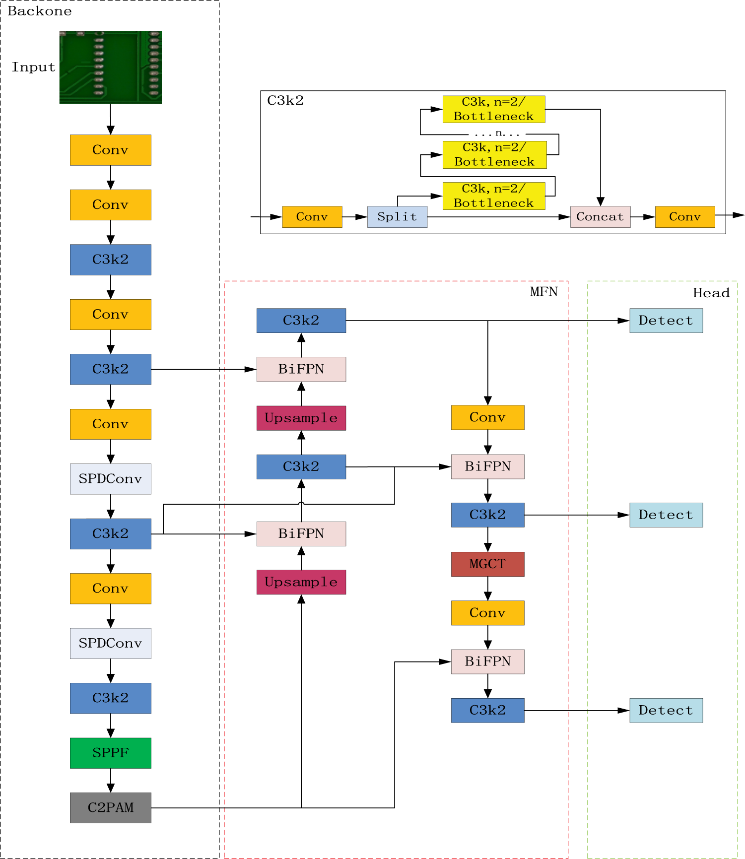
Figure 1: The overall architecture of SIM-Net
SPDConv is composed of an SPD layer and a non-strided convolution layer, designed as an alternative to conventional strided convolutions and pooling operations in CNNs. The SPD layer re-scales the input feature map by reducing its spatial resolution while expanding the channel dimension, thereby retaining information within the channel space. The subsequent non-strided convolution operates on each pixel or feature individually, primarily to adjust the number of channels. This design aims to preserve fine-grained details and minimize information loss.
Starting from the initial feature map X, the SPD layer first slices it into multiple sub-maps. Downsampling is then performed with a predefined scale factor, dividing X into
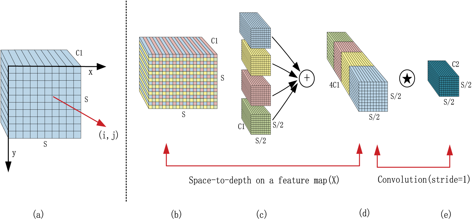
Figure 2: Illustration of SPDConv when the scale = 2
In this study, Within the YOLOv11 backbone, SPDConv is inserted after two convolutional layers. The first SPDConv mitigates the spatial information loss typically caused by traditional downsampling, compensating for the degradation of gradient features in the backbone. The second SPDConv complements the output feature map with subsequent upsampled features, thereby enhancing multi-scale semantic representation and improving cross-scale feature fusion. Compared with conventional convolution, SPDConv not only reduces spatial dimensionality but also achieves a higher degree of information retention in the channel dimension. This property significantly strengthens feature extraction, particularly for detecting small PCB defects.
3.3 Convolutional Partial Attention Module
Based on convolutional neural networks (CNN), PCB defect detection algorithms can extract multi-scale local features through convolutional kernels, enabling subtle differences in defect regions to be effectively captured. To address the difficulty of detecting small-sized PCB defects, this paper proposes a novel attention module, termed C2PAM. By integrating the C2PSA and CBAM mechanisms, C2PAM directs the network toward salient regions, enhances sensitivity to fine image details, and suppresses redundant information. Consequently, it improves the ability to detect objects across multiple scales and locations, while maintaining robustness in complex environments. The structure of C2PAM is illustrated in Fig. 3.
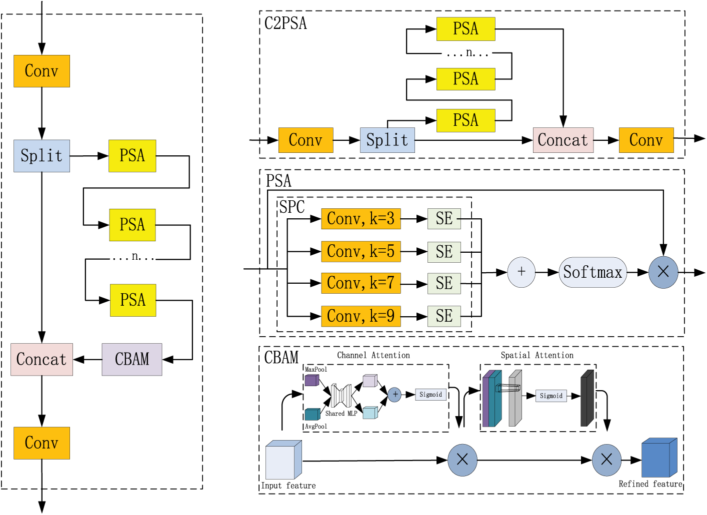
Figure 3: Illustration of the C2PAM module
The C2PSA module is an advanced feature extraction component embedded in YOLOv11. It strengthens multi-scale representation by combining the CSP structure with the pyramid squeeze attention (PSA) mechanism. PSA captures spatial information at different scales by employing convolutional kernels of varying sizes, while the squeeze-and-excitation (SE) operation adaptively reweights feature channels. This design improves the network’s focus on targets of diverse scales.
The CBAM module consists of two sequential submodules: channel attention and spatial attention. Given an input feature map, CBAM first generates a channel attention map and then a spatial attention map. By emphasizing informative features along both dimensions, CBAM adaptively refines representations through element-wise multiplication with the original feature map. This dual-level refinement enables the network to extract critical information more effectively, thereby enhancing PCB defect detection performance under complex background conditions.
3.4 Multi-Scale Fusion Network
The accurate detection of small PCB defects remains a significant technical challenge, not only because of the limited pixel information of small-scale targets but also due to the progressive attenuation of features as convolutional layers deepen. To address this issue, the MFN module is designed to substantially enhance small-object detection performance. MFN consists of two core components, BiFPN and MGCT, and is specifically tailored to strengthen feature fusion, emphasize the representation of small PCB defects, and improve the network’s ability to handle objects of varying sizes.
BiFPN is an advanced structure derived from feature pyramid networks (FPN) [26] and PANet. FPN employs a top-down hierarchical design to leverage contextual information and effectively capture small-target features. PANet extends this by introducing a bottom-up pathway to mitigate the limitation of one-way information flow. BiFPN further refines these designs by incorporating a weighted bidirectional feature fusion mechanism, enabling feature exchange across multiple levels and significantly improving multi-scale object processing. In addition, BiFPN establishes bidirectional connections between adjacent pyramid levels: high-resolution features are propagated upward through a bottom-up pathway, while low-resolution features are enhanced downward via a top-down pathway. This bidirectional flow allows the network to capture richer features across scales. Fig. 4 illustrates a comparison among three types of feature pyramid structures.
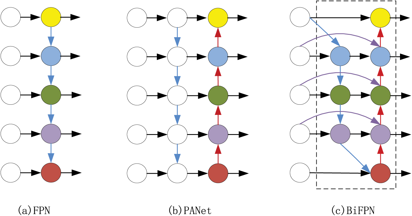
Figure 4: Comparison of three types of feature pyramid structures
The MGCT module, proposed in this study, is a lightweight and extensible component, as shown in Fig. 5. MGCT integrates DWConv with a channel attention mechanism (CAM) to expand the local receptive field and incorporate global contextual information. This design improves the network’s ability to recognize multi-scale objects while maintaining manageable computational complexity, making it suitable for practical deployment. When embedded into the BiFPN structure, MGCT enhances contextual modeling along the feature fusion pathways and significantly improves the efficiency of multi-scale feature interaction.
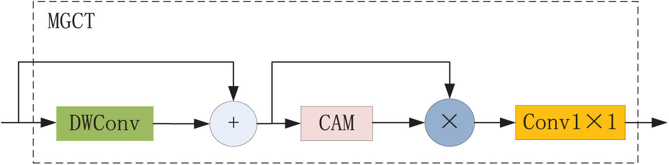
Figure 5: Illustration of the MGCT module
The public PCB defect dataset created by Peking University is comprised of 693 annotated images, covering six typical defect types: 115 missing holes, 115 mouse bites, 116 open circuits, 116 short circuits, 115 spurs, and 116 spurious copper defects, as illustrated in Fig. 6. However, due to the limited number of images and the small size of defect targets, this dataset poses certain challenges in model training and performance evaluation. To enhance dataset diversity and increase the number of images, an augmented dataset was created through various data augmentation techniques, including cropping, image flipping, mirroring, translation, image synthesis, and Gaussian blurring. The resulting dataset, which contains 8000 images, is allocated to training, validation, and testing phases in the proportion of 8:1:1. To further evaluate the generalization capability of the proposed model across different defect detection tasks, we conducted experiments on the NEU-DET steel surface defect dataset [27]. This dataset contains 1800 annotated images covering six common categories of steel surface defects, with 1260 images for training and 540 for testing.
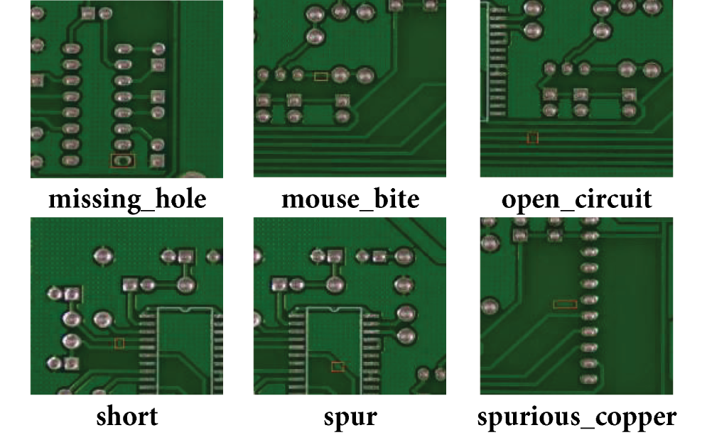
Figure 6: Six types of typical PCB defects
4.2 Experimental Environment and Evaluation Criteria
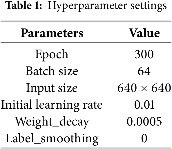
In this study, the experiments were carried out in a software environment comprising PyTorch 1.11.0, Python 3.8, Ubuntu 20.04, and CUDA 11.3. The hardware setup involved an NVIDIA GeForce RTX 4090 GPU (24 GB) and a 12 vCPU Intel(R) Xeon(R) Platinum 8352V CPU @ 2.10 GHz. The hyperparameters adopted for model training are summarized in Table 1. To evaluate the effectiveness of SIM-Net, we conducted comparative experiments against several widely used object detection models, including YOLOv5, YOLOv8, YOLOv10 [28], YOLOv11s, YOLOv11n, YOLOv12n, SSD, and Faster R-CNN. The comparison models were trained under the same hyperparameter settings as those applied for SIM-Net.
The evaluation metrics employed in this experiment to assess model performance include precision (P), recall (R), average precision (AP), mAP, F1 score, frames per second (FPS), parameter and floating-point operations per second (FLOPs). The above estimates will include true positives (TP), true negatives (TN), false positives (FP), and false negatives (FN), Among these metrics, TP represents the number of positive samples correctly identified, while TN denotes the number of negative samples accurately classified. FP corresponds to negative samples incorrectly predicted as positive, and FN refers to positive samples misclassified as negative.
The P measures the proportion of true positives among all predicted positives, thereby reflecting the model’s ability to minimize false positives. The formula for P is expressed as:
The R metric measures the proportion of correctly identified positive samples relative to all actual positives, thereby reflecting the model’s ability to detect all instances of a given class. The formula for R is expressed as:
AP evaluates the prediction accuracy for each class by integrating precision–recall curves. The formula for AP is given as:
As the mean value of the APs across all classes, the mAP provides a comprehensive measure of the model’s overall detection accuracy. The formula for mAP is expressed as:
The F1 score, defined as the harmonic mean of precision and recall, serves as a balanced indicator of model performance that accounts for both false positives and false negatives. The formula for F1 is:
As a metric representing the throughput of images processed per second, FPS reflects the computational speed of the model on a designated hardware platform, with higher values indicating faster detection capability. The parameter count represents the scale of learnable weights in the network, which directly affects the storage footprint and memory requirements of the model. FLOPs quantify the computational complexity of the model, with lower FLOPs indicating reduced computational burden and higher efficiency.
4.3 Experimental Analysis and Comparison
4.3.1 Experimental Validation of SPDConv
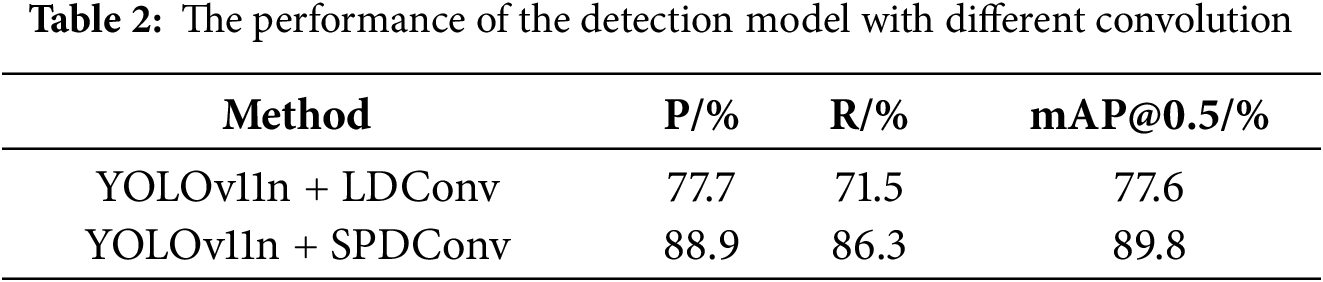
With SPDConv integrated into the model, the performance in detecting small PCB defects is enhanced. Unlike linear deformable convolution (LDConv) [29], which primarily focuses on adaptive receptive fields, SPDConv introduces spatially adaptive sampling while preserving structural consistency, thereby improving the model’s ability to capture fine-grained local features of small defects. To validate this approach, a comparative experiment was conducted against LDConv. Table 2 lists the results of detection performance comparison between incorporating SPDConv and LDConv into the YOLOv11n model. Apparently, YOLOv11n + SPDConv outperforms YOLOv11n + LDConv in precision, recall and mAP. These findings indicate that SPDConv is more suitable for enhancing YOLOv11n in PCB defect detection, particularly for small-scale defect scenarios.
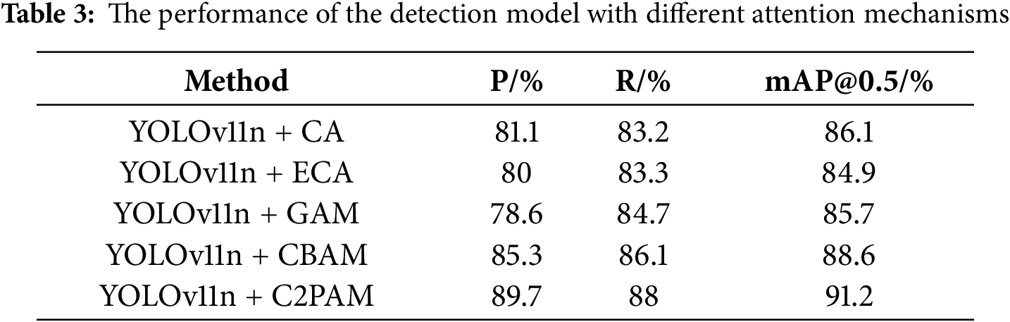
4.3.2 Experimental Validation of C2PAM
By incorporating the C2PAM attention mechanism, the negative impact of complex backgrounds is alleviated and the salient features of PCB surface defects are more effectively emphasized. In contrast to conventional attention modules such as coordinate attention (CA) [30], efficient channel attention (ECA) [31], global attention mechanism (GAM) [32], and CBAM, which tend to emphasize either channel or spatial information in isolation, C2PAM establishes a more comprehensive interaction between positional and spatial cues. This design enables the network to more accurately localize defect regions. In this study, C2PAM was compared with several commonly used attention mechanisms. As presented in Table 3, YOLOv11n + C2PAM achieves mAP@0.5 improvements of 5.1%, 6.3%, 5.5%, and 2.6% over YOLOv11n + CA, YOLOv11n + ECA, YOLOv11n + GAM, and YOLOv11n + CBAM, respectively, while also outperforming them in precision and recall. These results demonstrate that C2PAM effectively directs the network’s focus toward critical defect regions, thereby yielding superior detection performance in PCB surface defect inspection.
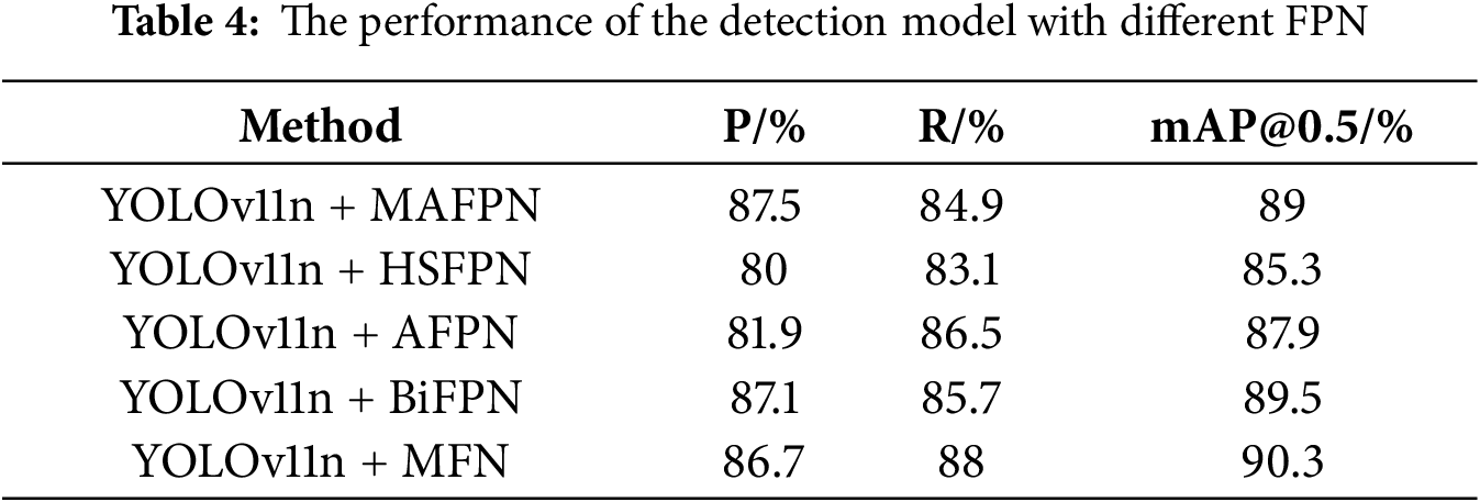
4.3.3 Experimental Validation of MFN
In the proposed method of PCB defect detection, multi-scale feature fusion plays a crucial role in capturing defects of varying sizes. The designed MFN enhances the integration of hierarchical features, enabling the network to retain fine-grained spatial details while simultaneously strengthening semantic representation across scales. To assess its effectiveness, MFN was compared with several representative FPN, including multi-branch auxiliary feature pyramid network (MAFPN) [33], high frequency and spatial perception feature pyramid network (HSFPN) [34], asymptotic feature pyramid network (AFPN) [35] and BiFPN. As reported in Table 4, although YOLOv11n + MFN yields slightly lower precision than YOLOv11n + MAFPN and YOLOv11n + BiFPN, it achieves superior recall and mAP compared with the other variants. These results indicate that MFN provides a more balanced trade-off between detection accuracy and robustness, making it particularly suitable for multi-scale PCB defect detection.
To quantify the contribution of each module to model performance, we conducted ablation experiments on the PCB defect dataset using SIM-Net. Six experimental configurations were designed, where “√” indicates the inclusion of a module and “×” denotes its absence, as summarized in Table 5. The results demonstrate that although the introduction of SPDConv slightly increased the number of parameters and computational cost, it effectively alleviated the loss of fine-grained features, leading to a 2.7% improvement in detection accuracy. Subsequently, the C2PAM attention mechanism, by focusing on multi-dimensional and multi-scale spatial information, significantly enhanced the model’s perception of complex backgrounds, improving recall by 2.2% and raising mAP@0.5 by 2%. Nevertheless, detecting small objects remains challenging due to limited pixel information. Finally, the MFN module further strengthened multi-scale feature fusion, boosting the model’s representational capacity and achieving an overall accuracy of 92% with an mAP@0.5 of 92.4%. Moreover, MFN not only enhanced multi-scale feature fusion but also reduced computational complexity. Notably, the FLOPs of the improved model are only 9.0, highlighting its efficiency while maintaining high detection accuracy.
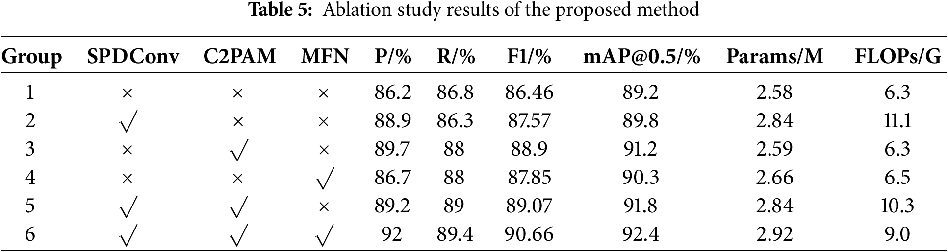
Compared with the baseline YOLOv11n, the proposed method achieved notable improvements: mAP@0.5 increased by 3.4%, precision by 5.8%, recall by 2.6%, and F1-score by 4.2%. As illustrated in Fig. 7, the enlarged area under the precision–recall curve further validates the effectiveness of the proposed approach. Overall, the analysis indicates that optimizing YOLOv11n with a single module yields limited gains, whereas the joint integration of SPDConv, C2PAM, and MFN provides complementary advantages, forming an efficient SIM-Net framework for PCB defect detection.
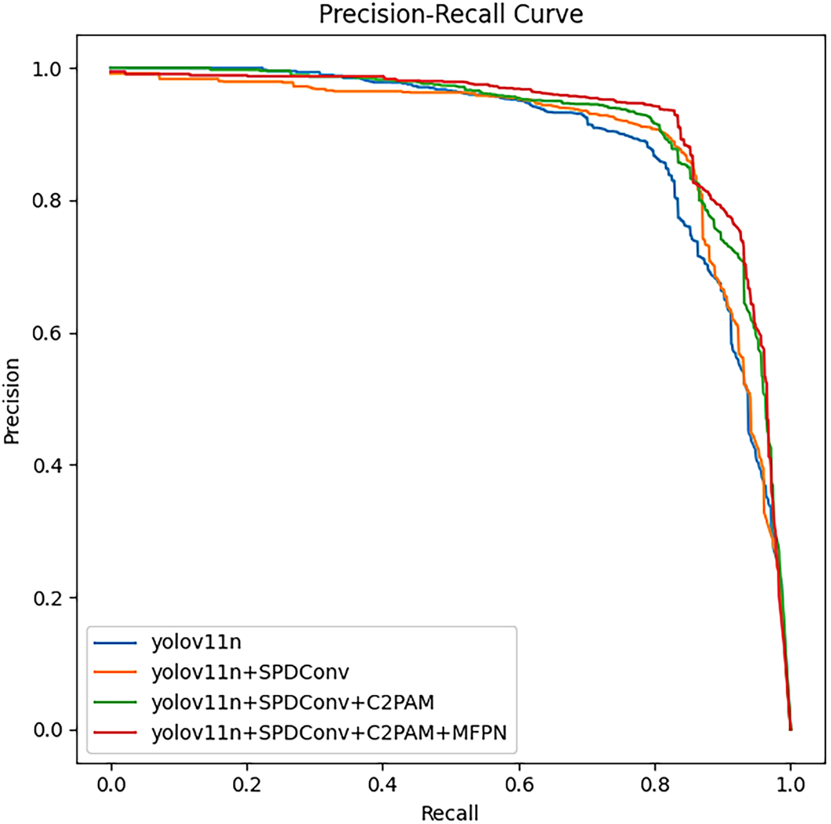
Figure 7: P-R curve
4.3.5 Comparison with Other Methods on PCB
To comprehensively evaluate the proposed method in terms of detection accuracy and lightweight characteristics, SIM-Net was compared with several state-of-the-art detectors, including Faster R-CNN, SSD, YOLOv5n, YOLOv8n, YOLOv10n, YOLOv11n, YOLOv11s, and YOLOv12n, under identical hyperparameter settings on the PCB surface defect dataset. As shown in Table 6, with only 2.92M parameters, the proposed SIM-Net method achieved a remarkably high mAP@0.5 of 92.4%, surpassing Faster R-CNN by 9.8%, SSD by 8.7%, YOLOv5n by 4.1%, YOLOv8n by 3.6%, YOLOv10n by 3.7%, YOLOv11n by 3.2%, YOLOv11s by 3.8%, and YOLOv12n by 2.9%. In addition, SIM-Net achieved a high inference speed of 75.1 FPS, which is 1.1 FPS faster than YOLOv11n, thereby satisfying the requirements of real-time PCB defect detection.
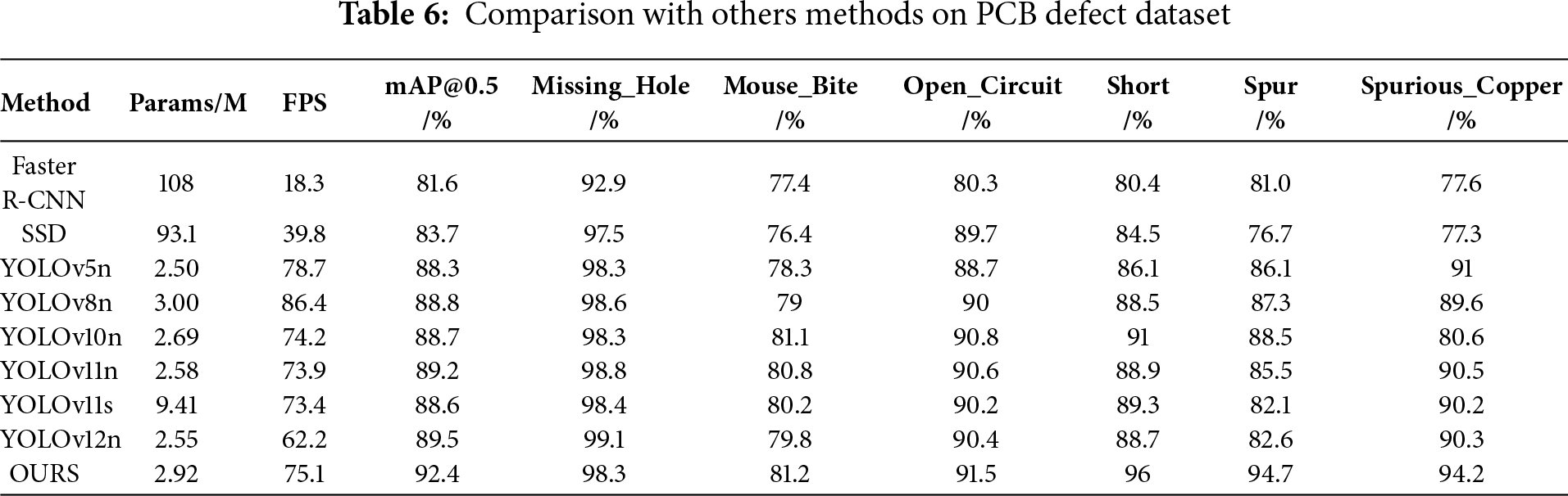
For each defect category, SIM-Net exhibits robust detection capability across diverse defect types, achieving particularly 96.0% for short, 94.7% for spurs, and 94.2% for spurious copper. Although the AP for mouse bites is relatively lower, it still surpasses most competing methods, indicating improved sensitivity to small and background-similar defects. In summary, the experimental results demonstrate that the proposed SIM-Net achieves consistent improvements in PCB defect detection, particularly for short circuits, spur, and spurious copper, where the gains are most pronounced. The method exhibits strong capability in identifying small-sized defects, while maintaining a favorable balance between detection accuracy, computational efficiency, and inference speed.
To further substantiate the effectiveness of the proposed SIM-Net, a visual comparison was conducted with nine representative models on the PCB defect dataset. As shown in the visualization results Fig. 8, most competing methods exhibited varying degrees of false or missed detections, particularly SSD, YOLOv10n, and YOLOv12n. In contrast, SIM-Net consistently produced accurate predictions across defects of different scales, with high confidence scores reinforcing the reliability of its outputs. These findings confirm that SIM-Net not only achieves superior quantitative performance but also demonstrates robust visual detection capability, thereby meeting the practical requirements of accurate and efficient PCB surface defect inspection.
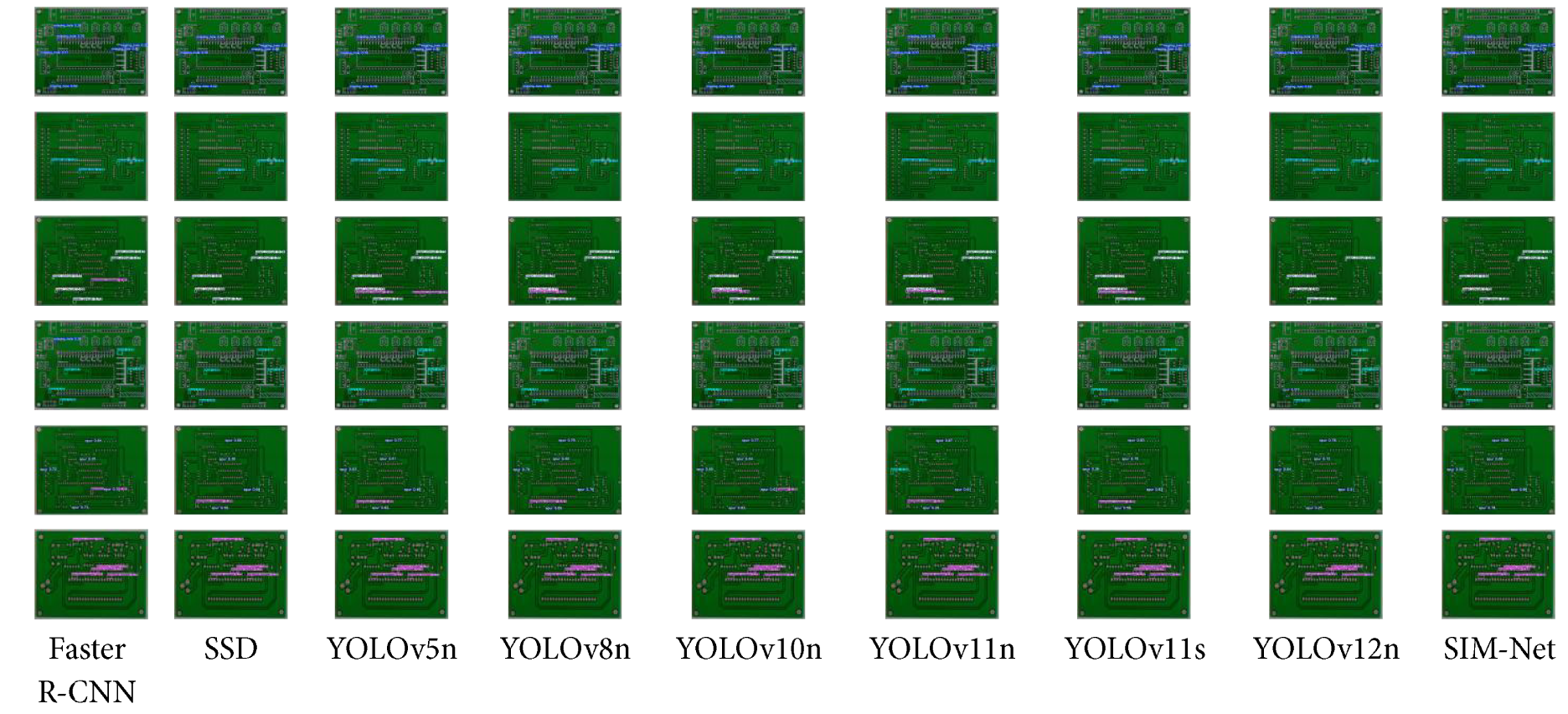
Figure 8: Six types of typical PCB defects
4.3.6 Comparison with Other Methods on NEU-DET
As shown in Table 7, the proposed model SIM-Net demonstrates superior overall performance on the NEU-DET dataset compared with several methods. Specifically, SIM-Net outperforms all models in this experiment, achieving 74.2% precision, 72.2% recall and 77.3%mAP@0.5. With only 2.92M parameters, the model also maintains a compact architecture. Although its detection speed is slightly lower than YOLOv5n and YOLOv8n, the achieved throughput remains sufficient for real-time industrial defect inspection. The detection visualizations Fig. 9 further confirm the robustness of SIM-Net, showing its ability to accurately localize and classify subtle and small-scale steel surface defects.
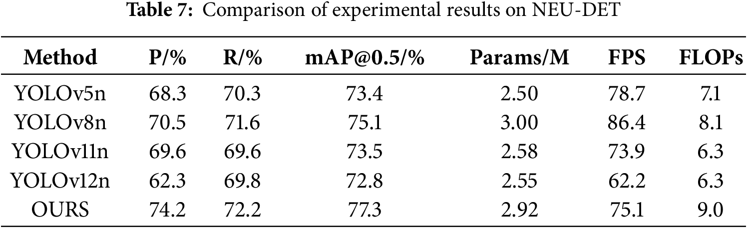
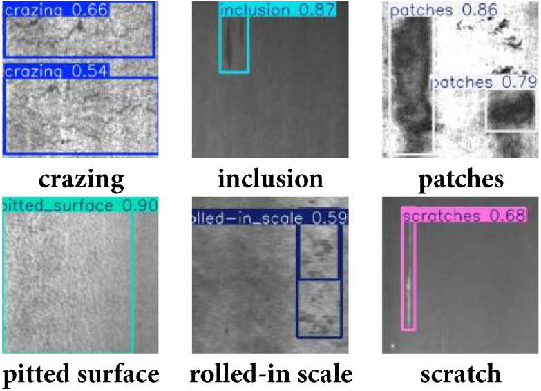
Figure 9: The detection visualizations on NEU-DET
In this paper, we propose an efficient and accurate method, termed SIM-Net, to address three major challenges in PCB surface defect detection: complex backgrounds, small defect sizes, and real-time requirements. First, the SPDConv module is introduced to mitigate the loss of fine-grained information by transforming spatial dimensions into channel dimensions, thereby preserving detailed features of small defects. Second, the C2PAM module is designed to capture subtle distinctions in defect regions by jointly exploiting channel and spatial information, which enhances the model’s discriminative capability under visually cluttered conditions. Finally, the MFN module is incorporated to strengthen multi-scale feature aggregation and accelerate inference, enabling more reliable detection of small-scale defects without sacrificing speed. Extensive experiments on a benchmark PCB defect dataset demonstrate that the proposed method achieves a mAP of 92.4%, while meeting real-time detection requirements and outperforming existing state-of-the-art approaches.
Despite its strong capability for rapid and accurate PCB defect detection, several limitations remain. The experimental dataset does not fully encompass the complete spectrum of defect categories, nor does it adequately represent highly complex or variable industrial environments. Moreover, research on model lightweighting and compression is still insufficient. Future work can proceed along two main directions. On the one hand, transfer learning may be employed to enrich the diversity and representativeness of PCB defect datasets, thereby improving robustness in scenarios involving rare defect types, intricate background textures, or domain shifts across production lines. This could involve cross-domain adaptation from related manufacturing datasets and the use of synthetic data generation to alleviate class imbalance. On the other hand, the computational demands of the model should be further reduced through advanced compression strategies, such as structured pruning, knowledge distillation, and quantization-aware training. These approaches would not only enhance detection efficiency but also enable low-latency, low-power deployment on edge devices, facilitating real-time quality inspection in resource-constrained industrial settings. Additionally, exploring hardware–algorithm co-optimization may further improve inference speed and energy efficiency, ensuring scalability for large-scale manufacturing applications.
Acknowledgement: The authors acknowledge the assistance of artificial intelligence tools in the language editing process, which contributed to improving the clarity and fluency of the manuscript.
Funding Statement: The authors received no specific funding for this study.
Author Contributions: The authors confirm contribution to the paper as follows: Conceptualization, Ping Fang; methodology, Ping Fang; validation, Ping Fang; investigation, Ping Fang; data curation, Ping Fang; writing—original draft preparation, Ping Fang; writing—review and editing, Mengjun Tong; visualization, Ping Fang; supervision, Mengjun Tong. All authors reviewed the results and approved the final version of the manuscript.
Availability of Data and Materials: The authors confirm that the data supporting the findings of this study are available within the article.
Ethics Approval: Not applicable.
Conflicts of Interest: The authors declare no conflicts of interest to report regarding the present study.
References
1. Zhang Q, Liu H. Multi-scale defect detection of printed circuit board based on feature pyramid network. In: Proceedings of the 2021 IEEE International Conference on Artificial Intelligence and Computer Applications (ICAICA); 2021 Jun 28–30; Dalian, China. p. 911–4. doi:10.1109/icaica52286.2021.9498174. [Google Scholar] [CrossRef]
2. Peng J, Yang Q, Chen D, Yang C, Xu Y, Qin Y. Dynamic SLAM visual odometry based on instance segmentation: a comprehensive review. Comput Mater Contin. 2024;78(1):167–96. doi:10.32604/cmc.2023.041900. [Google Scholar] [CrossRef]
3. Azamfirei V, Psarommatis F, Lagrosen Y. Application of automation for in-line quality inspection, a zero-defect manufacturing approach. J Manuf Syst. 2023;67(9):1–22. doi:10.1016/j.jmsy.2022.12.010. [Google Scholar] [CrossRef]
4. Deng YS, Luo AC, Dai MJ. Building an automatic defect verification system using deep neural network for PCB defect classification. In: Proceedings of the 2018 4th International Conference on Frontiers of Signal Processing (ICFSP); 2018 Sep 24–27; Poitiers, France. p. 145–9. doi:10.1109/ICFSP.2018.8552045. [Google Scholar] [CrossRef]
5. Shakiba FM, Shojaee M, Azizi SM, Zhou M. Real-time sensing and fault diagnosis for transmission lines. Int J Netw Dyn Intell. 2022;1(1):36–47. doi:10.53941/ijndi0101004. [Google Scholar] [CrossRef]
6. Jiang W, Li T, Zhang S, Chen W, Yang J. PCB defects target detection combining multi-scale and attention mechanism. Eng Appl Artif Intell. 2023;123(4968):106359. doi:10.1016/j.engappai.2023.106359. [Google Scholar] [CrossRef]
7. Zhang L, Chen J, Chen J, Wen Z, Zhou X. LDD-Net: lightweight printed circuit board defect detection network fusing multi-scale features. Eng Appl Artif Intell. 2024;129(4):107628. doi:10.1016/j.engappai.2023.107628. [Google Scholar] [CrossRef]
8. Sunkara R, Luo T. No more strided convolutions or pooling: a new CNN building block for low-resolution images and small objects. In: Machine learning and knowledge discovery in databases. Cham, Switzerland: Springer; 2023. p. 443–59. doi:10.1007/978-3-031-26409-2_27. [Google Scholar] [CrossRef]
9. Woo S, Park J, Lee JY, Kweon IS. CBAM: convolutional block attention module. In: Computer vision—ECCV 2018. Cham, Switzerland: Springer; 2018. p. 3–19. doi:10.1007/978-3-030-01234-2_1. [Google Scholar] [CrossRef]
10. Tan M, Pang R, Le QV. EfficientDet: scalable and efficient object detection. In: Proceedings of the 2020 IEEE/CVF Conference on Computer Vision and Pattern Recognition (CVPR); 2020 Jun 13–19; Seattle, WA, USA. p. 10778–87. doi:10.1109/cvpr42600.2020.01079. [Google Scholar] [CrossRef]
11. Hu X, Kong D, Liu X, Zhang J, Zhang D. Printed circuit board (PCB) surface micro defect detection model based on residual network with novel attention mechanism. Comput Mater Contin. 2024;78(1):915–33. doi:10.32604/cmc.2023.046376. [Google Scholar] [CrossRef]
12. Girshick R, Donahue J, Darrell T, Malik J. Rich feature hierarchies for accurate object detection and semantic segmentation. In: Proceedings of the 2014 IEEE Conference on Computer Vision and Pattern Recognition; 2014 Jun 23–28; Columbus, OH, USA. p. 580–7. doi:10.1109/CVPR.2014.81. [Google Scholar] [CrossRef]
13. Ren S, He K, Girshick R, Sun J. Faster R-CNN: towards real-time object detection with region proposal networks. IEEE Trans Pattern Anal Mach Intell. 2017;39(6):1137–49. doi:10.1109/TPAMI.2016.2577031. [Google Scholar] [PubMed] [CrossRef]
14. Hu B, Wang J. Detection of PCB surface defects with improved faster-RCNN and feature pyramid network. IEEE Access. 2020;8:108335–45. doi:10.1109/ACCESS.2020.3001349. [Google Scholar] [CrossRef]
15. Li YT, Kuo P, Guo JI. Automatic industry PCB board DIP process defect detection system based on deep ensemble self-adaption method. IEEE Trans Compon Packag Manuf Technol. 2021;11(2):312–23. doi:10.1109/TCPMT.2020.3047089. [Google Scholar] [CrossRef]
16. Li C, Xia W, Jiang Z. Weak feature defect generation with GAN for faster RCNN based PCB defect detection. In: Proceedings of the 2023 8th International Conference on Data Science in Cyberspace (DSC); 2023 Aug 18–20; Hefei, China. p. 306–12. doi:10.1109/DSC59305.2023.00051. [Google Scholar] [CrossRef]
17. Chen W, Su Y, Yang J. Split attention mechanism of faster RCNN for PCB defect detection. In: Proceedings of the 2024 International Conference on New Trends in Computational Intelligence (NTCI); 2024 Oct 18–20; Qingdao, China. p. 514–21. doi:10.1109/NTCI64025.2024.10776186. [Google Scholar] [CrossRef]
18. Redmon J, Divvala S, Girshick R, Farhadi A. You only look once: unified, real-time object detection. In: Proceedings of the 2016 IEEE Conference on Computer Vision and Pattern Recognition (CVPR); 2016 Jun 27–30; Las Vegas, NV, USA. p. 779–88. doi:10.1109/CVPR.2016.91. [Google Scholar] [CrossRef]
19. Khanam R, Hussain M. Yolov11: an overview of the key architectural enhancements. arXiv:2410.17725. 2024. doi:10.48550/arXiv.2410.17725. [Google Scholar] [CrossRef]
20. Liu W, Anguelov D, Erhan D, Szegedy C, Reed S, Fu CY, et al. SSD: single shot MultiBox detector. In: Computer vision—ECCV 2016. Cham, Switzerland: Springer; 2016. p. 21–37. doi:10.1007/978-3-319-46448-0_2. [Google Scholar] [CrossRef]
21. Wang X, Zhang Z, Xu Y, Zhang L, Yan R, Chen X. Real-time terahertz characterization of minor defects by the YOLOX-MSA network. IEEE Trans Instrum Meas. 2022;71(7):3521810. doi:10.1109/TIM.2022.3201945. [Google Scholar] [CrossRef]
22. Adibhatla VA, Chih HC, Hsu CC, Cheng J, Abbod MF, Shieh JS. Applying deep learning to defect detection in printed circuit boards via a newest model of you-only-look-once. Math Biosci Eng. 2021;18(4):4411–28. doi:10.3934/mbe.2021223. [Google Scholar] [PubMed] [CrossRef]
23. Liu G, Wen H. Printed circuit board defect detection based on MobileNet-Yolo-Fast. J Electron Imag. 2021;30(4):043004. doi:10.1117/1.jei.30.4.043004. [Google Scholar] [CrossRef]
24. Xiao G, Hou S, Zhou H. PCB defect detection algorithm based on CDI-YOLO. Sci Rep. 2024;14(1):7351. doi:10.1038/s41598-024-57491-3. [Google Scholar] [PubMed] [CrossRef]
25. Wang Y, Huang J, Dipu MSK, Zhao H, Gao S, Zhang H, et al. YOLO-RLC: an advanced target-detection algorithm for surface defects of printed circuit boards based on YOLOv5. Comput Mater Contin. 2024;80(3):4973–95. doi:10.32604/cmc.2024.055839. [Google Scholar] [CrossRef]
26. Lin TY, Dollár P, Girshick R, He K, Hariharan B, Belongie S. Feature pyramid networks for object detection. In: Proceedings of the 2017 IEEE Conference on Computer Vision and Pattern Recognition (CVPR); 2017 Jul 21–26; Honolulu, HI, USA. p. 936–44. doi:10.1109/CVPR.2017.106. [Google Scholar] [CrossRef]
27. He Y, Song K, Meng Q, Yan Y. An end-to-end steel surface defect detection approach via fusing multiple hierarchical features. IEEE Trans Instrum Meas. 2020;69(4):1493–504. doi:10.1109/TIM.2019.2915404. [Google Scholar] [CrossRef]
28. Chen H, Chen K, Ding G, Han J, Lin Z, Liu L, et al. YOLOv10: real-time end-to-end object detection. In: Proceedings of the Advances in Neural Information Processing Systems 37; 2024 Dec 10–15; Vancouver, BC, Canada. p. 107984–8011. doi:10.52202/079017-3429. [Google Scholar] [CrossRef]
29. Zhang X, Song Y, Song T, Yang D, Ye Y, Zhou J, et al. LDConv: linear deformable convolution for improving convolutional neural networks. Image Vis Comput. 2024;149(7–8):105190. doi:10.1016/j.imavis.2024.105190. [Google Scholar] [CrossRef]
30. Song W, Yan D, Yan J, Hu C, Wu W, Wang X. Ship detection and identification in SDGSAT-1 glimmer images based on the glimmer YOLO model. Int J Digit Earth. 2023;16(2):4687–706. doi:10.1080/17538947.2023.2277796. [Google Scholar] [CrossRef]
31. Hang J, Wu Y, Li Y, Lai T, Zhang J, Li Y. A deep learning semantic segmentation network with attention mechanism for concrete crack detection. Struct Health Monit. 2023;22(5):3006–26. doi:10.1177/14759217221126170. [Google Scholar] [CrossRef]
32. Liu Y, Shao Z, Hoffmann N. Global attention mechanism: retain information to enhance channel-spatial interactions. arXiv:2112.05561. 2021. doi:10.48550/arxiv.2112.05561. [Google Scholar] [CrossRef]
33. Yang Z, Guan Q, Zhao K, Yang J, Xu X, Long H, et al. Multi-branch auxiliary fusion YOLO with re-parameterization heterogeneous convolutional for accurate object detection. In: Pattern recognition and computer vision. Singapore: Springer; 2024. p. 492–505. doi:10.1007/978-981-97-8858-3_34. [Google Scholar] [CrossRef]
34. Shi Z, Hu J, Ren J, Ye H, Yuan X, Ouyang Y, et al. HS-FPN: high frequency and spatial perception FPN for tiny object detection. Proc AAAI Conf Artif Intell. 2025;39(7):6896–904. doi:10.1609/aaai.v39i7.32740. [Google Scholar] [CrossRef]
35. Yang G, Lei J, Zhu Z, Cheng S, Feng Z, Liang R. AFPN: asymptotic feature pyramid network for object detection. In: Proceedings of the 2023 IEEE International Conference on Systems, Man, and Cybernetics (SMC); 2023 Oct 1–4; Honolulu, HI, USA. p. 2184–9. doi:10.1109/SMC53992.2023.10394415. [Google Scholar] [CrossRef]
Cite This Article
 Copyright © 2026 The Author(s). Published by Tech Science Press.
This work is licensed under a Creative Commons Attribution 4.0 International License , which permits unrestricted use, distribution, and reproduction in any medium, provided the original work is properly cited.
 Downloads
 Citation Tools