
 Submit a Paper
 Propose a Special lssue
 Open Access
ARTICLE
Attention-Enhanced YOLOv8-Seg with WGAN-GP-Based Generative Data Augmentation for High-Precision Surface Defect Detection on Coarsely Ground SiC Wafers
Department of Mechanical Engineering, National Chin-Yi University of Technology, Taichung, Taiwan
* Corresponding Author: Chih-Yung Huang. Email:
Computers, Materials & Continua 2026, 87(2), 61 https://doi.org/10.32604/cmc.2026.075398
Received 31 October 2025; Accepted 07 January 2026; Issue published 12 March 2026
 View Full Text
 Download PDF
Abstract
Quality control plays a critical role in modern manufacturing. With the rapid development of electric vehicles, 5G communications, and the semiconductor industry, high-speed and high-precision detection of surface defects on silicon carbide (SiC) wafers has become essential. This study developed an automated inspection framework for identifying surface defects on SiC wafers during the coarse grinding stage. The complex machining textures on wafer surfaces hinder conventional machine vision models, often leading to misjudgment. To address this, deep learning algorithms were applied for defect classification. Because defects are rare and imbalanced across categories, data augmentation was performed using a Wasserstein generative adversarial network with gradient penalty (WGAN-GP), along with conventional methods. An improved YOLOv8-seg instance segmentation model was then trained and tested on datasets with different augmentation strategies. Experimental results showed that, when trained with WGAN-GP–generated data, YOLOv8-seg achieved mean average precision values of 87.0% (bounding box) and 86.6% (segmentation mask). Compared with the traditional WGAN-GP, the proposed model reduced Fréchet inception distance by 32.2% and multiscale structural similarity index by 29.8%, generating more realistic and diverse defect images. The proposed framework effectively improves defect detection accuracy under limited data conditions and shows strong potential for industrial applications.Keywords
Rapid advancements in electric vehicles, 5G communications, and the semiconductor industry have resulted in a growing demand for high-hardness materials that are resistant to high temperatures. This trend has accelerated the development of third-generation wide-bandgap compound semiconductors, which are primarily made of silicon carbide (SiC) and gallium nitride. Monocrystalline SiC wafers have emerged as the mainstream direction for the development of such conductors. SiC wafers exhibit excellent electrical and thermal stability, making them widely applicable in power devices and advanced processing technologies. The manufacturing process of SiC wafers involves multiple stages, including crystal growth, slicing, coarse grinding, fine grinding, and chemical mechanical polishing (CMP). In general, the production process for SiC wafers is similar to that of silicon wafers. However, the growth process of SiC ingots is substantially slower than that of Si ingots. For instance, approximately 7 days are required to prepare a SiC ingot that is sufficiently large for manufacturing 6-inch wafers (i.e., a diameter of 20–50 mm). After the crystal (ingot) growth process is completed, wire sawing is conducted to cut the ingots into wafers of suitable thickness for subsequent processing. The sawn wafers are subjected to grinding to remove the rough surface layer and damage caused by slicing while ensuring that they meet the required thickness and flatness. The grinding process consists of two primary stages: coarse grinding and fine grinding. Coarse grinding is performed using #2000-grit abrasive particles to rapidly remove a large quantity of material and eliminate deep subsurface damage. This process is followed by fine grinding using #4000–#8000-grit abrasives to further reduce surface roughness and improve surface quality and planarity. Subsequently, a final CMP process is performed to achieve high surface flatness and defect-free surfaces. Overall, the SiC wafer preparation sequence—comprising slicing, coarse grinding, fine grinding, and CMP—is highly sensitive to process parameters, where even minor deviations can cause surface defects that degrade wafer yield and quality. Implementing a defect-inspection mechanism immediately after the coarse-grinding stage enables early detection and correction, thereby preventing defect propagation, wafer breakage, and material loss.
Following the coarse grinding process, SiC wafers may exhibit defects caused by fabrication anomalies. For example, anomalies in the grinding wheel may lead to abrasive grain detachment, resulting in surface scratches, whereas excessive localized stress or inherent internal stress imbalance within the wafer may cause cracking (Fig. 1). Such defects not only compromise surface appearance but also trigger downstream process failures. For instance, if scratches remain on the surface during fine grinding, additional localized processing is often required to eliminate them. Although scratches are surface defects, when they penetrate the wafer’s stress equilibrium layer, they are highly likely to become fractures during high-load dynamic processes such as fine grinding or CMP. Similarly, cracks tend to expand during fine grinding or later stages (e.g., CMP or etching), potentially causing wafer breakage or total yield loss, which leads to severe economic losses and safety concerns. Rapid detection and elimination of such defects are therefore crucial for maximizing yield and minimizing financial loss. However, the wafer surface produced after coarse grinding contains highly complex and prominent machining textures, which can interfere with conventional machine vision algorithms and result in misjudgment during defect detection (Fig. 2). The complexity of this task is further underscored by a recent comprehensive review by Liu et al. [1], whose survey highlights that the industry is increasingly shifting towards deep learning-assisted visual inspection to handle such diverse defect morphologies and large-scale data throughput. With this shift, increasing research efforts have been directed toward integrating artificial intelligence (AI) into automated optical inspection (AOI) systems. In this context, You Only Look Once (YOLO) models have gained substantial attention for their high speed and detection accuracy. In particular, the YOLO version 8 (YOLOv8)-seg instance segmentation model demonstrates excellent performance in capturing fine features and identifying multiple types of defects. This model combines robust instance segmentation capabilities with a lightweight architecture, enabling simultaneous object localization and pixel-level segmentation. It achieves high detection accuracy under conditions involving noise and subtle defects, thus serving as a flexible and high-precision solution for complex industrial inspection tasks. Therefore, YOLOv8-seg was used in the present study to conduct precise evaluations of defect sizes, shapes, and distributions on SiC wafers.
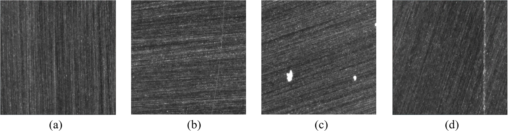
Figure 1: Examples of different defects on SiC wafers: (a) no defect, (b) scratches, (c) particle defects, and (d) cracks
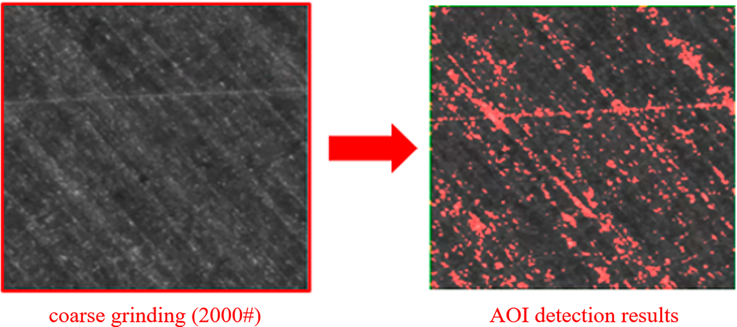
Figure 2: Inaccurate detection results caused by complex backgrounds in AOI
Because of the intrinsic properties of SiC, the probability of SiC-induced defects is extremely low, resulting in a limited number of annotated defect samples. This scarcity leads to challenges, particularly those related to data insufficiency and class imbalance in training deep learning models, restricting the practical deployment of these models in inspecting SiC wafer defects. Generative adversarial networks (GANs) [2] have emerged as a potential solution for solving this problem. Although conventional GANs exhibit strong data generation capabilities, they often exhibit training instability because of problems such as gradient vanishing. To mitigate such limitations, the Wasserstein GAN (WGAN) uses the earth mover’s distance as the loss function, thereby considerably improving both generation quality and convergence efficiency. An advanced WGAN model, namely WGAN with gradient penalty (WGAN-GP), replaces weight clipping with a gradient penalty mechanism to satisfy the Lipschitz continuity condition more rigorously. This modification enhances the model’s stability and accuracy when it processes high-dimensional data and complex background imagery; thus, the model can serve as a robust solution for defect data augmentation.
On the basis of the aforementioned discussion, the present study developed a wafer defect detection method that integrated an improved YOLOv8-seg model with a WGAN-GP-based generative data augmentation strategy. The contributions of this research are as follows:
1. To address the problems caused by scale variations and complex backgrounds in wafer defect detection, this study enhanced the YOLOv8-seg model by introducing an efficient multiscale attention (EMA) mechanism into the C2f and SPPF modules of the backbone network. Moreover, the conventional path aggregation network (PAN)–feature pyramid network (FPN) structure was replaced with a bidirectional FPN (BiFPN), thus improving channel–spatial interaction and multilevel feature fusion.
2. To mitigate the problems of data scarcity and class imbalance among different types of defects, this study used the WGAN-GP model in combination with an online data augmentation module. This setup enabled real-time generation and expansion of target-class images during training, thereby effectively increasing data diversity and balance.
3. By integrating the aforementioned model optimization and data augmentation strategies, this study established a deep learning framework that balanced detection accuracy and data augmentation capabilities. Experimental results indicated that the proposed framework outperformed the YOLOv8-seg model and conventional data augmentation approaches in terms of mean average precision (mAP), results obtained with the Toolkit for Identifying Detection and Segmentation Errors (TIDE), and visualized outputs, highlighting its practical utility and value in the detection of wafer surface defects.
The remainder of this paper is organized as follows. Section 2 reviews AI applications used for defect detection and GAN-based methods for addressing data imbalance. Section 3 introduces the WGAN-GP and YOLOv8-seg models and details the improvements proposed in this study. Section 4 describes the experimental setup of this study, the adopted defect dataset, and the empirical validation of the proposed method. Finally, Section 5 provides the conclusions of this study.
This section reviews existing research on industrial surface defect detection technologies, focusing on two main aspects. First, it outlines the current state and development trends of AI-based defect detection. Second, it details the methods and findings of studies that have used GANs to address data imbalance; and summarizes the corresponding strategies and techniques proposed in the literature.
2.1 Applications of AI in Defect Detection
With the rapid advancements in AI technologies, deep learning has demonstrated considerable potential and practical value in the field of industrial defect detection. Object detection is a foundational step in AI-enabled defect detection, enabling the accurate localization and identification of target defects within images. However, object detection methods only provide bounding box information, which causes difficulty in precisely delineating defect shapes and achieving pixel-level localization. This limitation causes a major problem in manufacturing processes, which require accurate assessments of defect locations and shapes. Instance segmentation algorithms have emerged as potential solutions to this problem, facilitating high-precision pixel-level segmentation of target objects. Instance segmentation methods are of two types: one-stage methods and two-stage methods (e.g., Mask Region-Based Convolutional Neural Network (R-CNN) [3], PANet [4], and PointRend [5]). One-stage methods, such as YOLO [6], have real-time object detection capabilities. YOLACT [7] is a real-time instance segmentation model based on the YOLO framework. Instead of predicting raw masks for each individual instance, YOLACT generates a set of prototype masks for the entire image and then predicts linear combination coefficients for each detected instance. YOLO version 5 (YOLOv5)-seg [8] is an extension of the YOLOv5 model that supports both pixel-level mask generation and bounding box prediction. Similarly, YOLO version 7 (YOLOv7)-seg [9] is an extension of the YOLOv7 model that is specifically designed for instance segmentation tasks. These models have been widely applied in defect detection. Ferguson et al. proposed a defect detection system based on Mask R-CNN combined with transfer learning for identifying casting and welding defects in X-ray images. To address the industry-wide challenge of limited defect data, they compared the performance of their system when it was trained on the ImageNet and COCO datasets with and without transfer learning [10]. Fondevik et al. investigated the performance of automated approaches involving instance segmentation for the detection of corrosion damage. They found that the Mask R-CNN and PSPNet models achieved mean Intersection-over-Union scores of 77.5% and 73.2%, respectively, on a dedicated defect dataset. Their results confirmed the strong potential of using segmentation models for the inspection of industrial steel structures and suggested that instance segmentation is more suitable than semantic segmentation in diverse real-world scenarios [11]. Prathyuksha et al. compared the performance of the Mask R-CNN and YOLOv8-seg models in leather defect detection. Their results indicated that compared with the Mask R-CNN model, YOLOv8 exhibited higher efficiency in detecting defects of varying sizes and shapes and achieved more accurate predictions by using fewer training data samples. YOLOv8 achieved a mAP of 99.2%, which was considerably higher than that of the Mask R-CNN model (i.e., 92%). Thus, YOLOv8 is a promising solution for quality inspection in the leather industry [12]. Recent studies have further adapted and optimized YOLOv8 for industrial surface defect inspection. For example, You and Kong [13] reported an improved YOLOv8-based method for steel surface defect detection, demonstrating the continued competitiveness of YOLOv8 variants in industrial scenarios. Tang et al. [14] also proposed an enhanced YOLOv8-based architecture for chip surface defect detection and reported favorable accuracy-efficiency trade-offs. In parallel, DETR-style Transformer detectors such as RT-DETR [15] and RF-DETR [16] have been explored for real-time detection tasks. Motivated by these trends, this study adopts YOLOv8-seg as the base instance segmentation model and introduces lightweight attention and feature-fusion enhancements to balance pixel-level accuracy and computational efficiency for SiC wafer inspection.
2.2 Research on Addressing Data Imbalance by Using GANs
GAN models have demonstrated remarkable generative capabilities in the field of image processing, emerging as prominent tools for image syntheses and data augmentation. The GAN architecture, which was proposed by Goodfellow et al., comprises a generator and discriminator, which are trained through an adversarial process that enables the generator to learn and approximate the distribution of real data [2]. Various extensions of the original GAN model have been developed to enhance generation quality and training stability. For instance, the deep convolutional GAN [17] model employs a CNN architecture to improve model convergence and stability. The WGAN model [18] uses the earth mover’s distance as a loss function, thus effectively alleviating the problem of gradient vanishing, which is commonly observed in conventional GANs. Furthermore, WGAN-GP [19] builds upon the WGAN framework by incorporating a gradient penalty term to constrain the discriminator’s variation range more rigorously, thereby enhancing training stability and the quality of generated outputs. Because of their excellent capabilities in learning distributions and synthesizing realistic images, GANs have been widely applied in data augmentation tasks. They are particularly effective in addressing challenges such as data scarcity and class imbalance in industrial settings and have become one of the most commonly used generative models in the field of deep learning today.
Chen et al. employed a GAN model to address the imbalance between defect-free and defect-containing images of silicon dies. By augmenting the collected image dataset with synthesized defect images, they successfully enhanced the generalization capability of their classification model. In a subsequent study, they integrated their GAN framework with the YOLO version 3 (YOLOv3) architecture to develop an automated detection method for wafer surface defects, which substantially improved the model’s ability to identify subtle defects [20]. Demirci et al. proposed a hybrid data augmentation strategy that involves combining the WGAN-GP model with an online data augmentation module to generate electroluminescence images of solar cells. This approach allowed a pretrained VGG-16 model to achieve an accuracy of 94.11% in the classification of solar cell defects given limited data. Thus, integrating a GAN model, particularly the WGAN-GP model, with online augmentation mechanisms can effectively enhance the accuracy and practical applicability of deep learning models in industrial defect detection tasks [21]. Dewi et al. synthesized traffic sign images by using deep convolutional GAN, least squares GAN, and WGAN models and then used these images in the training of YOLO version 4 (YOLOv4) and YOLOv3 models for detecting traffic signs. Their experiments indicated that among the aforementioned GAN models, the least squares GAN exhibited the highest structural similarity index (SSIM) of 0.498, which substantially improved the accuracy of YOLOv4 to 89.33% [22]. An et al. focused on the detection of defects in insulator cap components within the overhead contact systems of high-speed railway networks, where defect samples are difficult to obtain. They used the WGAN-GP model to generate high-quality defect images and then combined this model with YOLOv5 and ResNet50 for defect localization and classification, respectively. Their method improved the recall from 82.1% to 94% and the accuracy to 97.1%, thus outperforming conventional data augmentation methods [23]. Addressing data scarcity and class imbalance remains a central challenge in industrial AI. Li et al. [24] demonstrated that synthetic data augmentation can effectively improve defect analysis performance when only limited real samples are available. Recently, diffusion-based synthesis has also been explored for defect data generation; for example, Qiu et al. [25] proposed a diffusion-based approach for wafer defect image generation in semiconductor manufacturing. In addition, Leiñena et al. [26] showed that latent diffusion models can enhance the performance of visual defect segmentation networks in steel surface inspection. Meanwhile, GAN-based augmentation remains attractive due to its relatively lower computational cost and practical deployment. Hu et al. [27] reported GAN-based data augmentation for semiconductor wafer dicing induced defects under limited data, and Jeganathan [28] discussed a transformer-based and generative-AI framework for semiconductor wafer inspection. Motivated by these studies, we adopt an optimized WGAN-GP framework with online data augmentation to generate diverse defect samples for robust training under data-limited industrial scenarios.
The methodological design aims to address critical challenges in industrial defect inspection, such as data scarcity, class imbalance, and complex multiscale surface textures. This study integrates generative data augmentation and an improved segmentation network to enhance detection accuracy and generalization. The method comprises three main components: Section 3.1 Generative Data Augmentation and the WGAN-GP Model, Section 3.2 Improved YOLOv8-Seg Model, and Section 3.3 Overall Framework for surface defect detection on silicon carbide wafers.
3.1 Generative Data Augmentation and the WGAN-GP Model
Defects rarely occur during SiC wafer grinding, and the occurrence probabilities of different defect types vary considerably, resulting in insufficient data and severe class imbalance. To address these issues, the Wasserstein GAN with Gradient Penalty (WGAN-GP) model was employed for data augmentation. A GAN consists of a generator and a discriminator that are trained adversarial to produce synthetic data resembling real samples. In the original GAN framework, the discriminator uses a sigmoid activation function to minimize the Jensen–Shannon (JS) divergence between real and generated distributions. However, if the discriminator trains too well and perfectly separates the two distributions, the JS divergence becomes a constant (saturates), causing the gradients backpropagated to the generator to vanish. This phenomenon, known as the vanishing gradient problem, makes training unstable and difficult. In contrast, WGAN replaces the JS divergence with the Earth-Mover (Wasserstein) distance to measure the difference between the real data distribution
where
where
Crucially, the Wasserstein metric yields non-vanishing gradients only if the 1-Lipschitz constraint is satisfied. The original WGAN enforced this by clipping the discriminator’s weights to a small fixed range. By bounding the weights, the Lipschitz constant is constrained, ensuring the mathematical validity of the Wasserstein distance and preventing gradient saturation. However, this forced clipping may hinder convergence and limit the discriminator’s capacity. Therefore, WGAN-GP replaces weight clipping with a gradient penalty term, defined in (5), with the loss function of its generator being the same as that of the WGAN model (4).
where x, z,
To further enhance the diversity and realism of generated defect images, an online data augmentation module was incorporated into the WGAN-GP architecture, as illustrated in Fig. 3. During each training iteration, real samples are randomly flipped or brightness-adjusted, exposing the discriminator to a broader range of “real” variations. This encourages the generator to compete with a more robust discriminator, thereby improving the fidelity and diversity of synthesized images and mitigating overfitting.
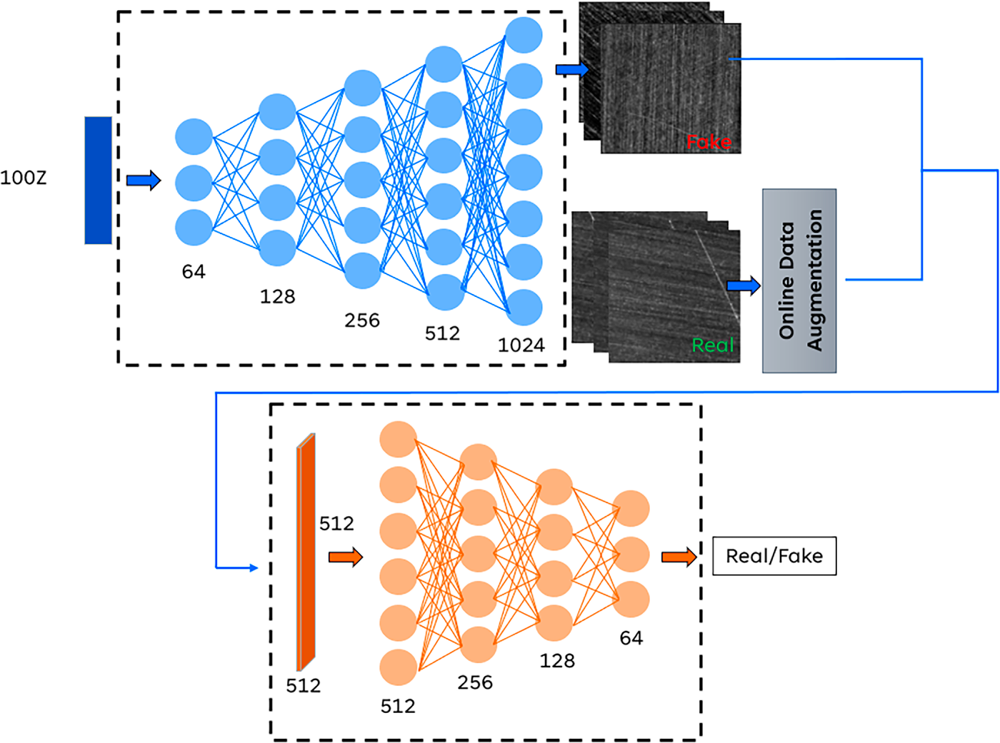
Figure 3: Architecture of the proposed WGAN-GP model
The WGAN-GP model was trained using the RMSProp optimizer with a learning rate of 0.0001, a batch size of 5, and 20,000 epochs. During the training phase, the input noise vector
YOLOv8-seg, developed by Ultralytics, is a significant advancement in instance segmentation that preserves the efficiency of the single-stage YOLO framework while incorporating anchor-free detection and decoupled heads. The architecture of the original YOLOv8-seg model is illustrated in Fig. 4. However, detecting surface defects on SiC wafers remains challenging due to large variations in defect scale, complex background textures, and visual similarities among defect types. To address these challenges, we introduce two critical architectural enhancements to the standard YOLOv8-seg network: the Efficient Multi-Scale Attention (EMA) module and the Bidirectional Feature Pyramid Network (BiFPN). The overall structure of the improved model, integrating these optimization modules, is presented in Fig. 5.
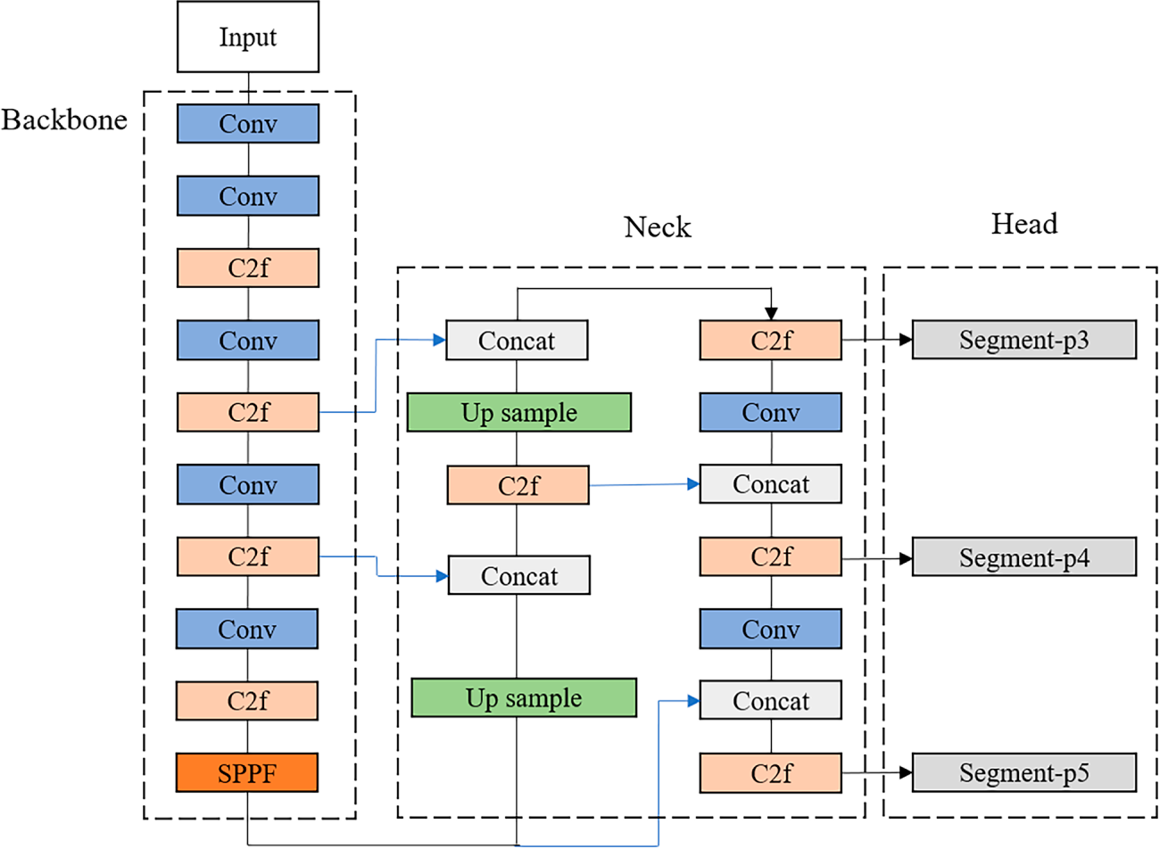
Figure 4: Architecture of the original YOLOv8-seg model
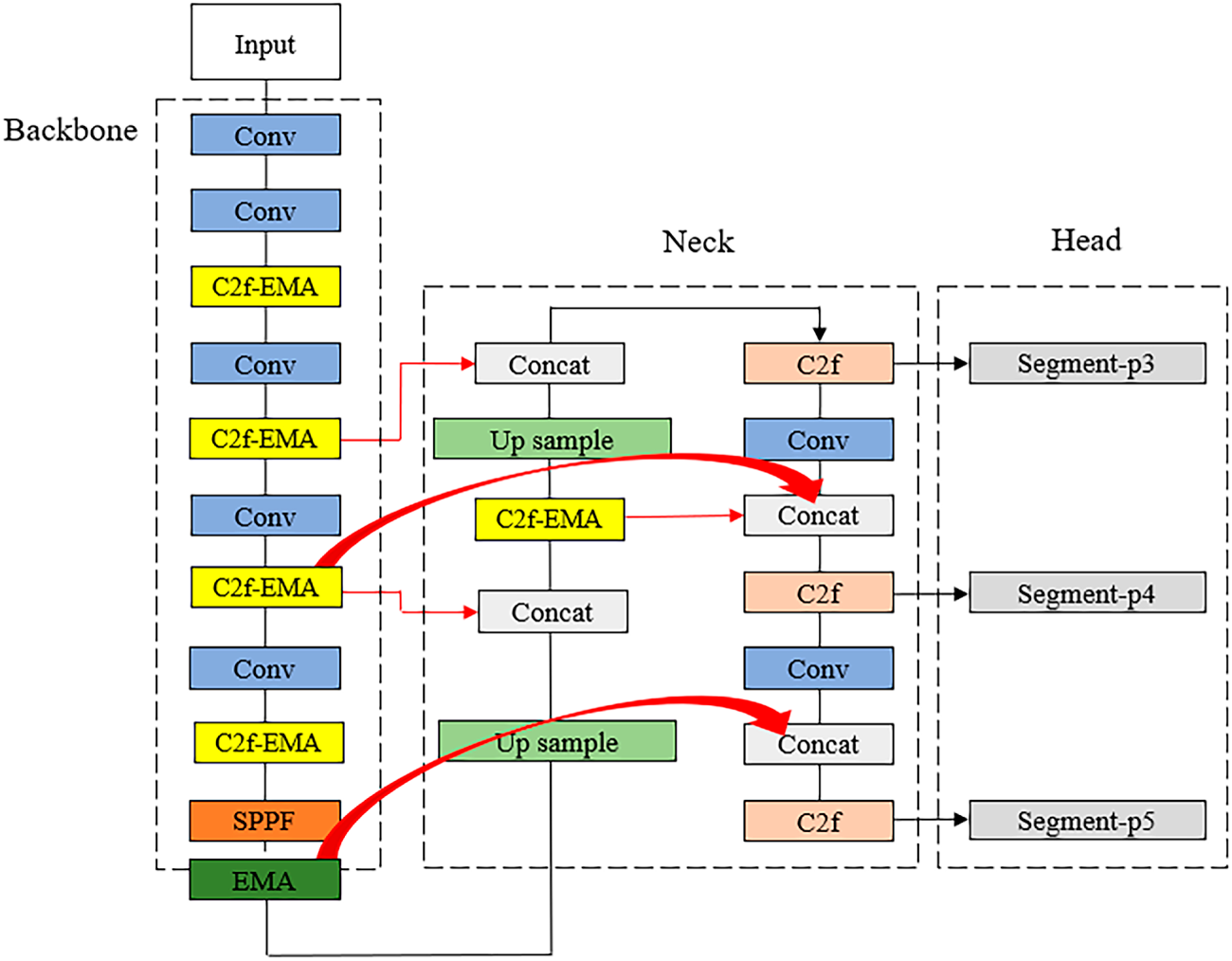
Figure 5: Architecture of the improved YOLOv8-seg model
3.2.1 Efficient Multi-Scale Attention (EMA) Module
Surface defects on SiC wafers vary greatly in scale, shape, and appearance, complicating feature extraction and localization. To address this and enhance the YOLOv8-seg model’s ability to represent multiscale features, EMA modules [29] were incorporated at two key locations: one combined with the C2f module (C2f–EMA) and another with the SPPF module. The detailed integration of EMA within the network architecture is illustrated in Fig. 6b. The EMA module is an advanced attention mechanism designed to model interdependencies between channel and spatial dimensions without incurring high computational costs. Mathematically, for an input feature map
(a) Feature Grouping. The module first divides the feature map along the channel dimension into
(b) Parallel Subnetworks and Encoding. Within each sub-group, EMA employs three parallel branches to extract attention. Two branches utilize 1D global average pooling to encode spatial information along the horizontal and vertical directions, respectively. These operations capture long-range dependencies and are mathematically expressed as:
where
(c) Cross-Spatial Learning. To achieve robust feature aggregation, the EMA module fuses the global features (from the
where
Figure 6: First stage of YOLOv8-seg optimization: (a) EMA module and (b) application of EMA in the YOLOv8-seg network
3.2.2 Bidirectional Feature Pyramid Network (BiFPN)
In multiscale object detection tasks, optimizing the flow and fusion of information across feature maps of varying resolutions is critical for elevating the model’s overall feature extraction capabilities. Although the original YOLOv8s-seg employs an FPN-based architecture for multilevel feature integration, its PAN–FPN structure exhibits increasing limitations, such as inefficiencies in cross-layer information propagation and loss of semantic details as the network depth increases. To overcome these limitations, the present study incorporated a BiFPN into the neck of the YOLOv8s-seg model. A structural comparison between the conventional PAN–FPN and the adopted BiFPN is presented in Fig. 7. Compared with the PAN–FPN architecture, BiFPN utilizes bidirectional (i.e., top-down and bottom-up) feature fusion paths and integrates learnable weights to adaptively balance the importance of information at each layer [30]. Mathematically, for a given node in the feature network, let
where
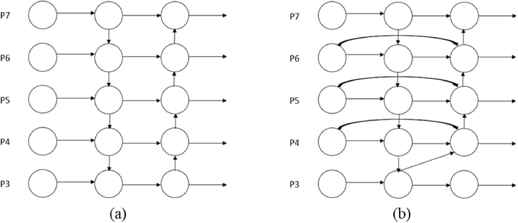
Figure 7: Comparison between the PAN–FPN and BiFPN architectures
These two enhancements jointly elevate the precision of YOLOv8-seg in localization and mask prediction for SiC wafer surface defects.
The framework integrates the WGAN-GP model with online data augmentation to address data scarcity and class imbalance, and the improved YOLOv8-seg with C2f–EMA, SPPF–EMA, and BiFPN modules to enhance multiscale feature recognition and detection accuracy (see Fig. 8). It is important to note that the WGAN-GP model is employed exclusively during the training phase to expand the dataset. In the actual inference phase (industrial application), the WGAN-GP module is deactivated, and the trained YOLOv8-seg model directly processes real input images to detect defects.
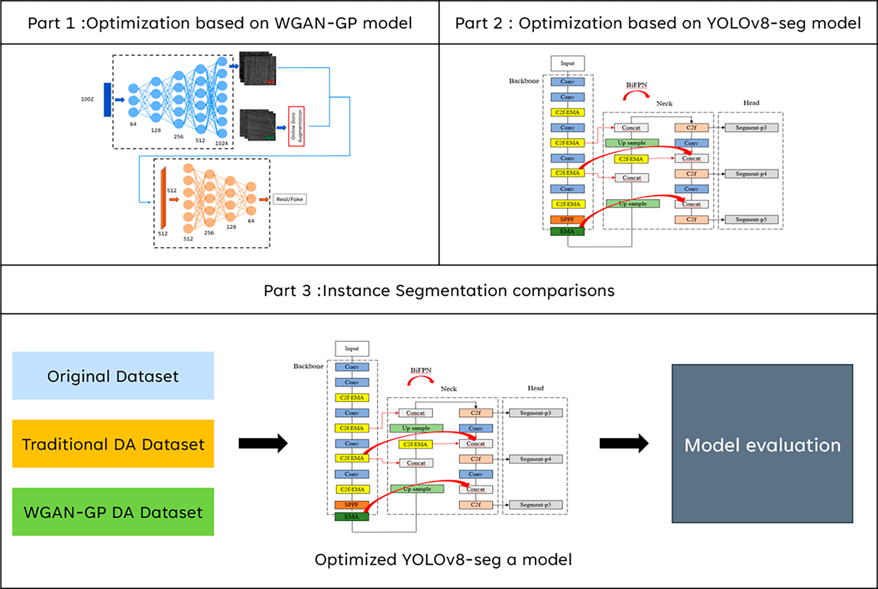
Figure 8: Complete architecture of the proposed framework. Note that Part 1 (WGAN-GP) is utilized solely for offline data augmentation during training, while Part 2 and Part 3 represent the detection pipeline and evaluation
Before presenting the specific results and detailed discussions, this section provides an overview of the experimental setup, data configuration, and evaluation metrics used to validate the proposed approach. The aim is to ensure that the analysis of findings is well-grounded in the experimental framework and that each result can be accurately interpreted based on the established methodology. By outlining the experimental conditions and validation strategy, the subsequent discussion of results covering performance metrics, visual comparisons, and model behavior can be clearly contextualized and effectively linked to the objectives of this study.
4.1 Experimental Data and Preprocessing
The wafer defect dataset used in this study was collected from 31 SiC wafers exhibiting surface defects of three main categories: scratches, particle defects, and cracks. These defects primarily originate from variations in material processing conditions. Scratches occur when abrasive particles detach from the grinding wheel and damage the wafer surface; particle defects arise from dust or fibers retained on the wafer; and cracks are caused by localized strain during the grinding process. Because of the high hardness of SiC wafers, scratch defects are relatively rare, resulting in severe class imbalance (132 scratch images versus 530 particle and 530 crack images). The optical inspection system used for image acquisition is shown in Fig. 9. It consists of an XYZ servo motor platform equipped with a linear scale (resolution = 0.5 μm) and a 5-megapixel PiA2400-17gm industrial camera with a 4.5× zoom lens. A ring light source was used for top-down illumination, providing an optical resolution of 0.766 μm/pixel and a field of view of approximately 1.8 × 1.8 mm2.
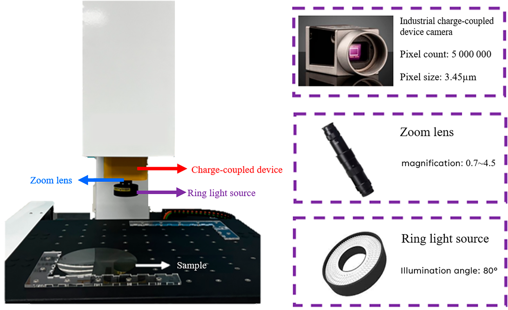
Figure 9: Imaging system used in this study
Example wafer defect images are presented in Fig. 10. Among the three types of defects, only particle defects can be removed through surface cleaning, whereas scratches and cracks cause irreversible damage that makes wafers unsuitable for downstream processing.
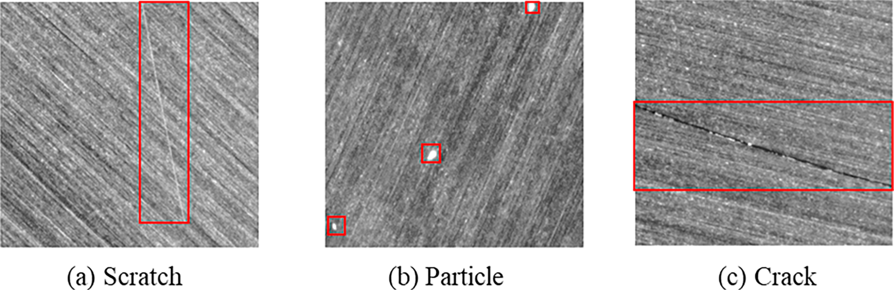
Figure 10: Example images of different types of wafer defects
The original images (resolution = 2464 × 2046 pixels) were resized to 1024 × 1024 pixels and divided into 512 × 512-pixel subimages to improve training efficiency and ensure consistent defect localization. After preprocessing, a total of 1192 defect images were obtained. The number of samples in each defect category is summarized in Table 1.
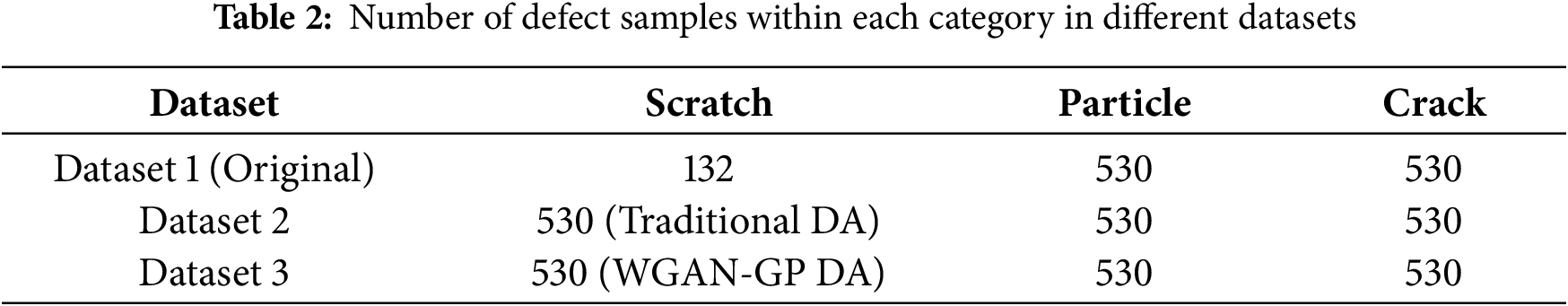
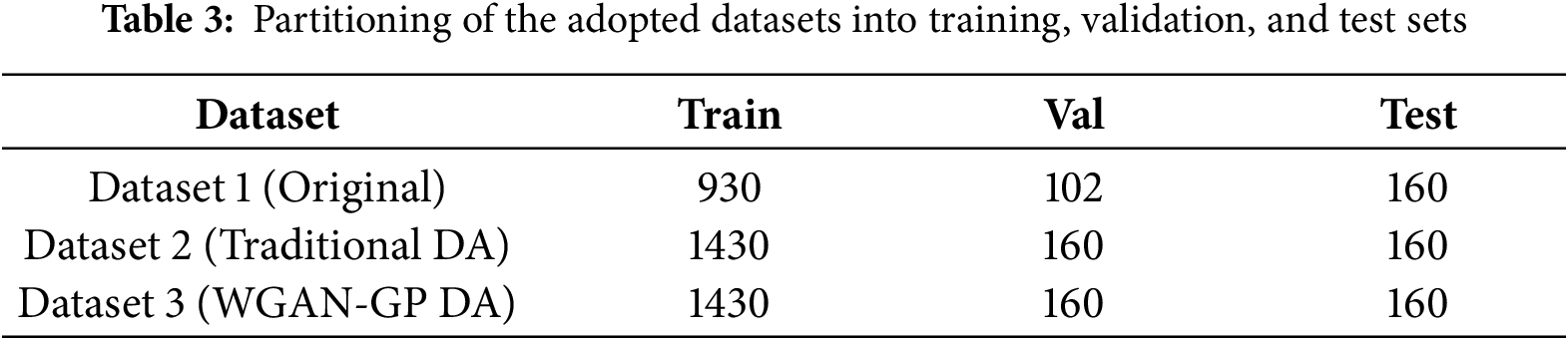
To address the data imbalance and enrich feature diversity, three distinct datasets, namely Datasets 1–3, were constructed in this study for comparative evaluation. Dataset 1 contained only the original images. Dataset 2 contained the original images and new images produced through non-geometric transformation and traditional data augmentation methods, such as random horizontal and vertical flipping, grayscale adjustment, and contrast modification. Finally, Dataset 3 contained the original images and new images generated for scratches by using the WGAN-GP model proposed in this study. Details regarding the three datasets are presented in Table 2.
4.2 Experimental Configuration and Evaluation Criteria
The experiments were conducted in Python using the PyTorch (version 2.1.1) deep learning framework. All training and inference procedures were executed on a workstation equipped with an Intel Core i9-13900K processor, 128 GB RAM, and an NVIDIA GeForce RTX 4080 GPU (16 GB VRAM) under Windows 10, with CUDA 11.8 providing GPU acceleration.
4.2.1 Detection Model Configuration and Data Partitioning
To rigorously evaluate the impact of different data-augmentation strategies, the YOLOv8-seg model was trained on the three constructed datasets (Datasets 1, 2, and 3). To ensure a fair comparison and verify the model’s robustness under complex conditions, a fixed test set of 160 images was reserved prior to any training or data augmentation process. These test samples were specifically selected to include multi-type defects, simulating challenging real-world inspection scenarios where multiple defect categories co-exist within a single field of view. Crucially, this test set was strictly isolated and never exposed to either the YOLOv8-seg model during detection training or the WGAN-GP model during the generative phase, thereby preventing data leakage. The remaining 1032 original images were allocated for training and validation purposes in Dataset 1. For Datasets 2 and 3, additional augmented and synthetic samples were incorporated into the training sets, while the reserved test set remained unchanged. The specific distributions are summarized in Table 3. Consequently, all experimental results reported in this study are based on this identical, independent test set, ensuring that the evaluation reflects true generalization performance rather than the memorization of synthetic features. Following the data preparation, the detection model was configured for optimal training stability. The proposed YOLOv8s-seg model was trained under the following hyperparameter settings: a learning rate of 0.001, stochastic gradient descent (SGD) as the optimizer, a batch size of 16, and a total of 300 training epochs. The performance of the trained model was systematically evaluated using the mean Average Precision (mAP) metric on the fixed test set.
4.2.2 Generative Model Configuration (WGAN-GP)
To compensate for the limited scratch samples and enhance feature diversity, a WGAN-GP model was trained with the RMSProp optimizer (learning rate = 0.0001, batch size = 5, epochs = 20,000). The generated images were evaluated by Fréchet Inception Distance (FID) [31] and multiscale structural similarity (MS-SSIM) [32], where lower values indicate higher realism and greater diversity. The corresponding formulas are as follows:
For the generative model, FID and MS-SSIM jointly quantified the realism and diversity of generated samples. For the detection model, mAP provided a comprehensive measure of detection accuracy across categories. To further interpret model behavior, the TIDE (Tool for Identifying Detection Errors) framework was adopted for detailed error analysis [33]. While mAP gives an overall accuracy measure, TIDE classifies and quantifies six types of detection errors—classification, localization, compound, duplicate, background false positives, and missed detections, the latter being most critical in industrial defect inspection. A schematic of the TIDE framework is shown in Fig. 11.
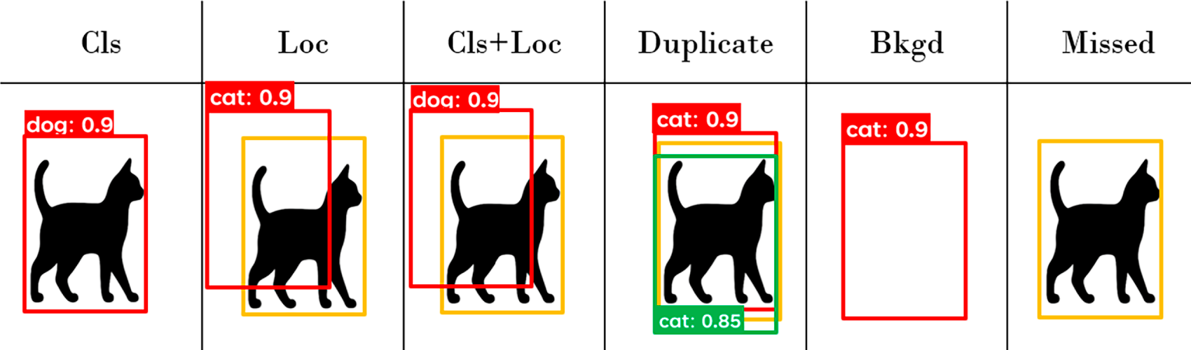
Figure 11: Schematic of the TIDE framework
4.3 Performance Analysis of the Generative Model
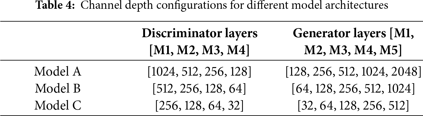
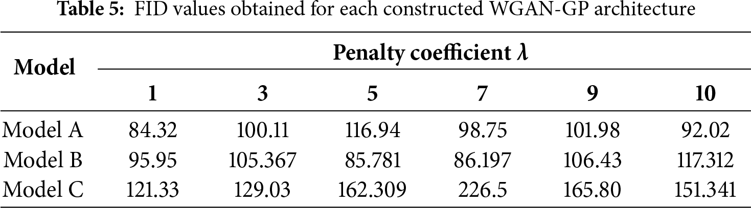
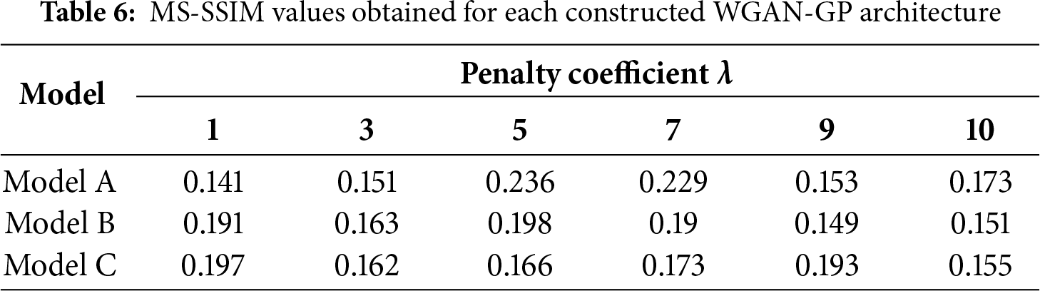
Based on the experimental configuration described previously, the performance of the proposed generative model was quantitatively and qualitatively evaluated to verify its effectiveness in synthesizing realistic and diverse scratch defects. Three WGAN-GP architectures (Models A–C) with different channel depth configurations were constructed, as summarized in Table 4, and each model was trained under six penalty coefficients (λ = 1, 3, 5, 7, 9, 10).
The quantitative results of the experiments are presented in Tables 5 and 6, which indicate that Model A with λ = 1 achieved the lowest FID and MS-SSIM values, corresponding to the most realistic and diverse generated images. Therefore, this configuration was adopted as the final version of the proposed WGAN-GP model.
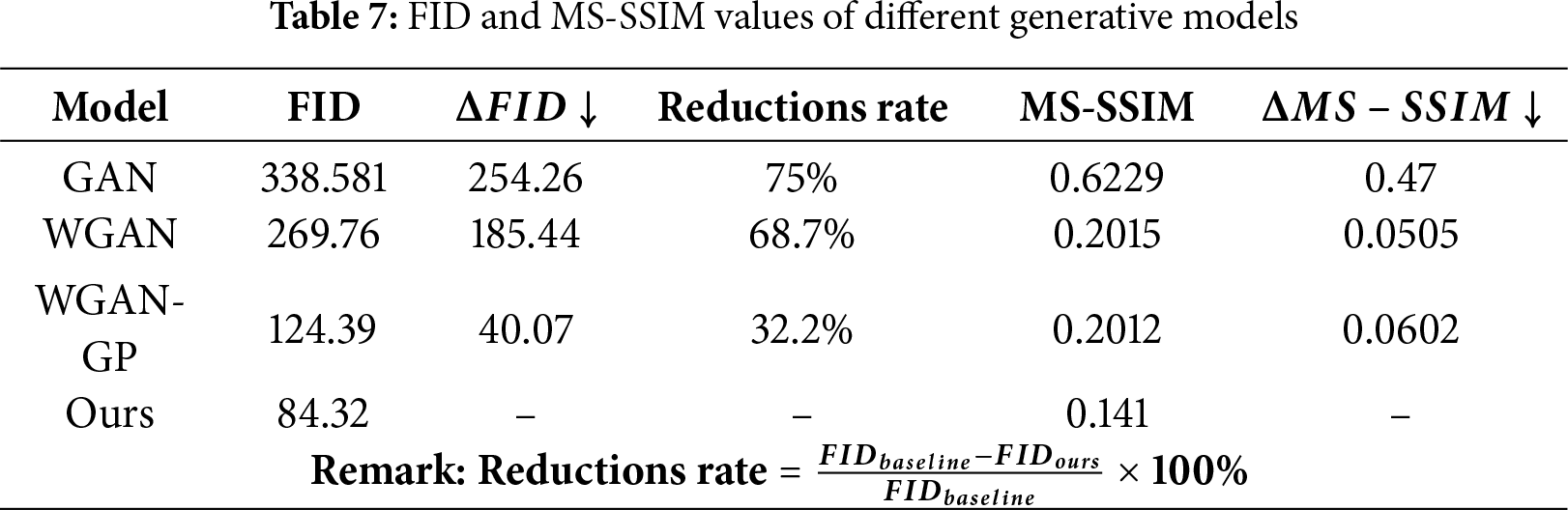
Compared with the baseline generative models, the proposed WGAN-GP exhibited substantial quantitative improvements, as summarized in Table 7. The FID decreased from 124.39 to 84.32 (−32.2%), and the MS-SSIM decreased from 0.2012 to 0.141 (−29.8%), demonstrating that the proposed model generated images with higher realism and greater structural diversity than conventional GAN, WGAN, or the original WGAN-GP.
Beyond numerical improvements, visual inspection further confirmed the superiority of the proposed model. As shown in Fig. 12, conventional GANs often produced blurred or incomplete textures, whereas WGAN improved stability but still exhibited artifacts caused by weight clipping. The original WGAN-GP generated clearer structures but lacked sample diversity. By contrast, the proposed WGAN-GP combined with online data augmentation produced defect images that were both structurally consistent and texturally diverse, most closely resembling real scratch defects.
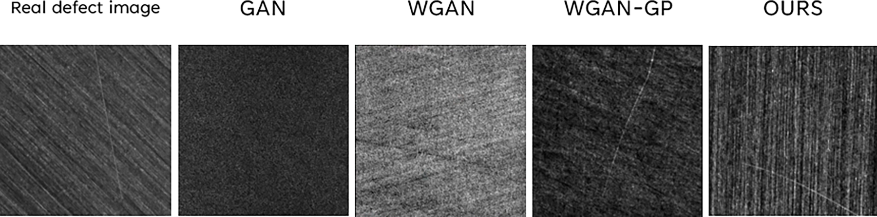
Figure 12: Defect images generated by different GAN architectures
Together, these quantitative and qualitative results confirm that the proposed WGAN-GP framework not only improves image quality but also effectively enhances data diversity, providing a balanced and representative training set for the subsequent defect-detection experiments. The effectiveness of the generated data was further validated through downstream detection experiments, as discussed in the following section.
4.4 Overall Detection Performance Evaluation
This section presents a comprehensive evaluation of the proposed defect detection framework, focusing on both architectural optimization and the impact of generative data augmentation. The analyses include ablation experiments, comparative performance benchmarking, and error-type decomposition using TIDE. Together, these evaluations aim to verify the accuracy, efficiency, and robustness of the proposed YOLOv8-seg–based detection system under complex wafer surface conditions.
4.4.1 Effectiveness of Structural Optimization
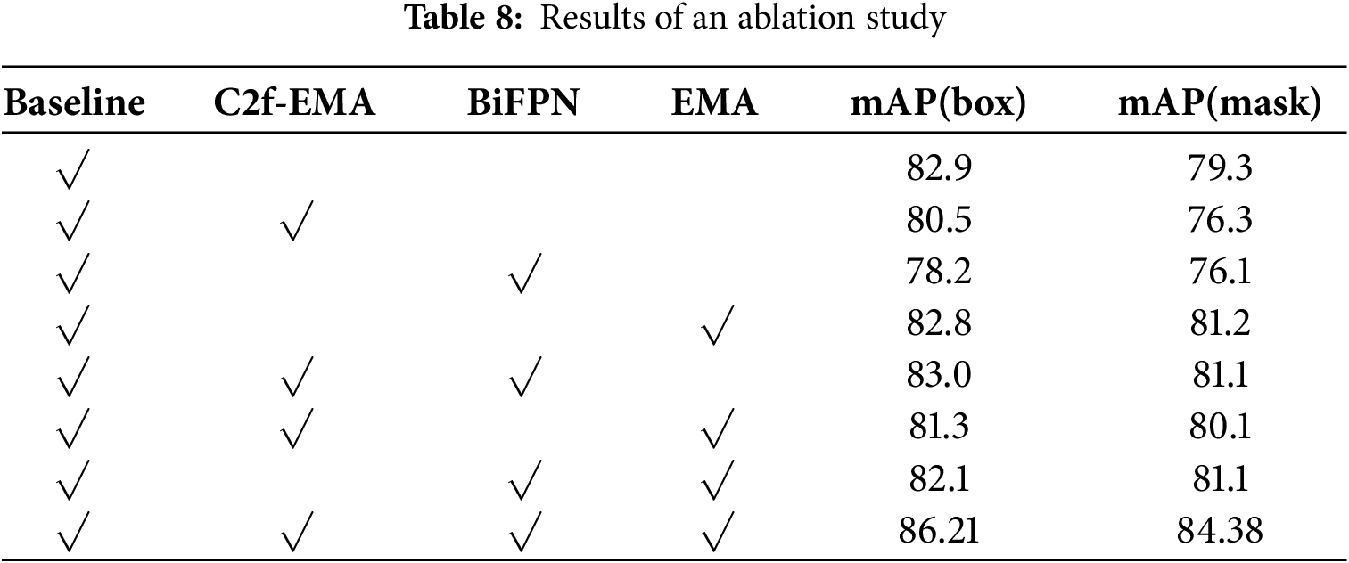
To verify the contribution of architectural enhancements (EMA and BiFPN) in the proposed YOLOv8-seg model, an ablation study was conducted. The results, summarized in Table 8, show that the combined modifications improved mAP(box) by 3.31% and mAP(mask) by 5.08% compared with the baseline YOLOv8s-seg model, indicating that the enhanced structure provides more stable and accurate detection under complex surface conditions.
As shown in Fig. 13, the baseline model often missed subtle defects, whereas the proposed model detected them more completely, demonstrating improved robustness and accuracy under complex conditions.
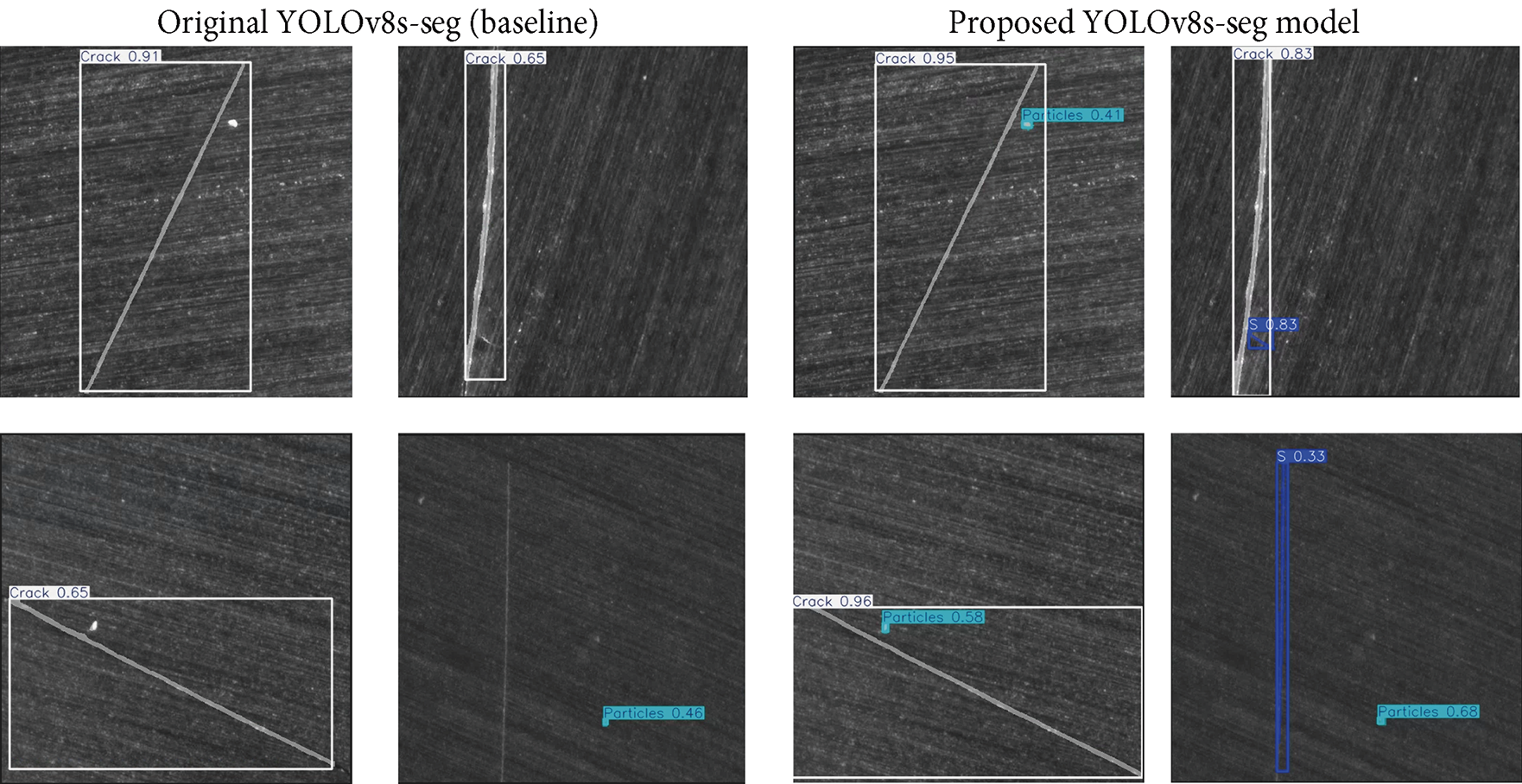
Figure 13: Detection results obtained using the baseline and proposed YOLOv8s-seg models
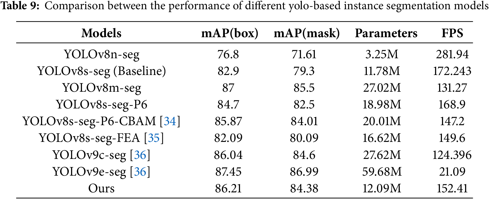
4.4.2 Efficiency and Complexity-Performance Trade-Off Analysis
To strictly evaluate the cost-effectiveness of the proposed improvements, we analyzed the trade-off between model complexity (parameters and inference speed) and detection performance, as summarized in Table 9. Regarding the complexity of the attention mechanism, although incorporating the EMA module introduces additional matrix multiplications and coordinate encoding operations, its lightweight design ensures limited computational overhead. Specifically, a detailed comparison with the baseline reveals that the integration of EMA and BiFPN increased the parameter count by only 2.6% (from 11.78M to 12.09M). Despite this modest increase in model size, the detection accuracy improved significantly, with mAP(box) increasing by 3.31% (from 82.9% to 86.21%) and mAP(mask) increasing by 5.08% (from 79.3% to 84.38%). Furthermore, while the inference speed decreased by approximately 11.5% (from 172.24 FPS to 152.41 FPS) due to the added computational layers, the speed remains significantly higher than the typical industrial requirement of 30–60 FPS. These results empirically justify the increase in complexity, as the slight parameter growth yields a clear gain in precision, which is critical for identifying irreversible defects on SiC wafers. In comparison with other mainstream models, the proposed framework demonstrates superior efficiency. Although YOLOv8m-seg and YOLOv9e-seg [36] exhibited slightly higher mAP(box) (87% and 87.45%, respectively) and mAP(mask) (85.5% and 86.99%, respectively) than did the proposed model, these gains came at the cost of a considerable increase in model complexity and computational load. Specifically, YOLOv8m-seg and YOLOv9e-seg [36] required approximately 27.22 and 59.68 million parameters, respectively, which were more than two times and slightly less than five times higher than those required by the proposed model. Moreover, these two models had markedly lower inference speeds (131.27 and 21.09 FPS, respectively) compared to the proposed model (152.41 FPS). In summary, the experimental results indicate that the proposed model achieves competitive detection accuracy to that of high-performing YOLO-based models while using significantly fewer parameters and maintaining high inference speeds. This favorable balance between performance and computational efficiency confirms the proposed model’s strong potential for deployment in real-time industrial defect inspection scenarios.
4.4.3 Comparison with Representative Non-Yolo Models
To comprehensively validate the competitiveness of the proposed method beyond the YOLO framework, the evaluation was extended to include a diverse range of representative non-YOLO models. These include the classic two-stage Mask R-CNN [3], real-time one-stage models (SOLOv2 [37], Yolact [7]), and state-of-the-art (SOTA) Transformer-based architectures (Mask2Former [38], RF-DETR [16]). All comparative experiments were conducted on Dataset 2 (with traditional data augmentation) under an identical hardware environment (single NVIDIA RTX 4080 GPU). The quantitative results are summarized in Table 10.
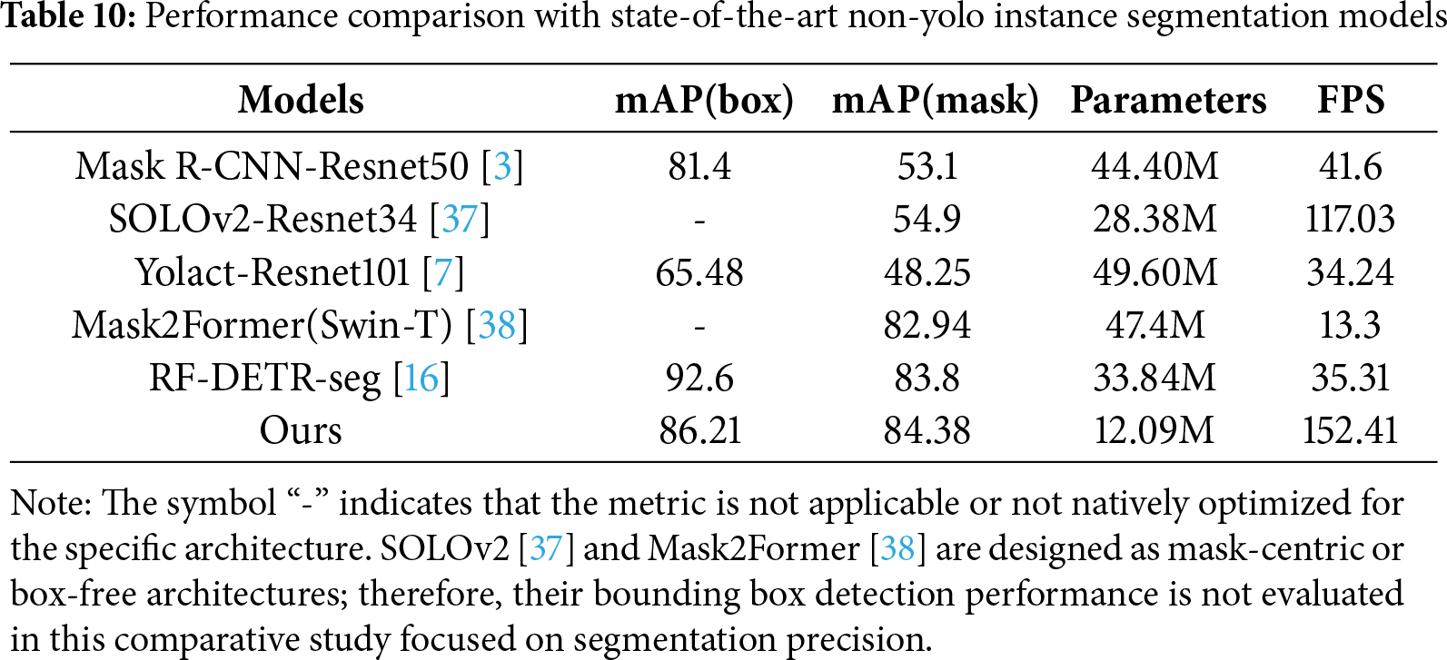
Segmentation Accuracy and Robustness As evidenced in Table 10, the proposed improved YOLOv8-seg model demonstrates superior segmentation performance compared to both traditional CNN-based and modern Transformer-based baselines. Against the classic Mask R-CNN, our method achieved a substantial improvement in mAP(mask), rising from 53.1% to 84.38%, highlighting the limitations of the two-stage baseline in handling complex industrial textures. Furthermore, while the Transformer-based RF-DETR-seg exhibited a high detection accuracy (mAP(box) of 92.6%), the proposed model outperformed it in the critical segmentation metric, achieving a higher mAP(mask) of 84.38% compared to 83.8% for RF-DETR-seg and 82.94% for Mask2Former. This result indicates that despite having significantly fewer parameters (12.09M), the proposed feature fusion and attention mechanisms enable more precise defect boundary delineation than the computationally heavy Transformer models. Computational Efficiency and Training Costs For practical industrial deployment, inference speed and training efficiency are as critical as accuracy. In terms of inference, the proposed model operates at 152.41 FPS, which is 4× to 11× faster than RF-DETR-seg (35.31 FPS) and Mask2Former (13.3 FPS), ensuring seamless integration into high-speed production lines.
Moreover, a significant disparity in computational cost was observed during training. Due to the high memory consumption inherent to Transformer architectures, Mask2Former and RF-DETR-seg were trained with a batch size of 4. We observed that these models converged relatively quickly; thus, training was conducted for 100 epochs to ensure optimal performance without overfitting, and the best validation checkpoint was selected for comparison. Despite the fewer epochs, the total training time required was 12 and 21 h, respectively. In stark contrast, the proposed lightweight model supported a batch size of 16 and completed 300 epochs in under one hour. This 20× to 60× higher training efficiency makes the proposed method far more practical for real-world scenarios where frequent model retraining is necessary for new defect types.
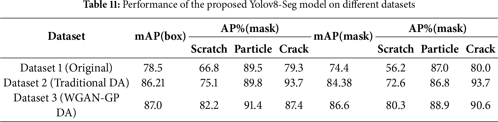
4.4.4 Effectiveness of Generative Data Augmentation
The influence of different data-augmentation strategies on detection performance is presented in Table 11. When trained with Dataset 3 (WGAN-GP DA), the proposed model achieved the best results, reaching mAP(box) = 87.0% and mAP(mask) = 86.6%, outperforming both the baseline and traditional augmentation settings. These results demonstrate that the synthetic scratch samples generated by the WGAN-GP effectively mitigate class imbalance and enhance model generalization.
A detailed error analysis using TIDE was conducted to further verify the robustness of the proposed framework. As shown in Fig. 14, the framework substantially reduced missed-detection rates, which represent the most critical error type in industrial inspection. Specifically, the miss rate for bounding boxes decreased from 25.12% to 18.14% (−6.98%), and that for segmentation masks decreased from 25.62% to 16.39% (−9.23%). Although other error types exhibited minor variations, the marked reduction in missed detections demonstrates that the proposed framework achieves higher detection stability and reliability while maintaining real-time efficiency.
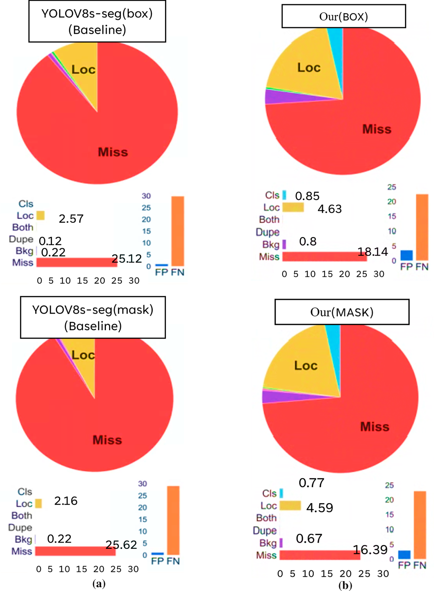
Figure 14: Detection and segmentation errors obtained through TIDE analyses for the (a) baseline YOLOv8s-seg model and (b) the proposed framework (improved YOLOv8s-seg + improved WGAN-GP)
4.5 Generalizability Verification on Public Industrial Datasets
To further assess the robustness and generalizability of the proposed framework beyond the specific context of SiC wafer inspection, extensive validation experiments were conducted on three widely recognized public industrial defect datasets: Magnetic-tile-defect [39], NEU-seg [40], and DAGM 2007 [41]. These datasets were specifically selected as they share critical characteristics with SiC wafer imagery, including complex surface textures, low contrast between defects and background, and diverse defect scales (as illustrated in Fig. 15). Comparative experiments were performed against the baseline YOLOv8s-seg model to verify whether the proposed improvements—specifically the attention mechanisms and feature fusion modules—maintain their effectiveness across different domains.
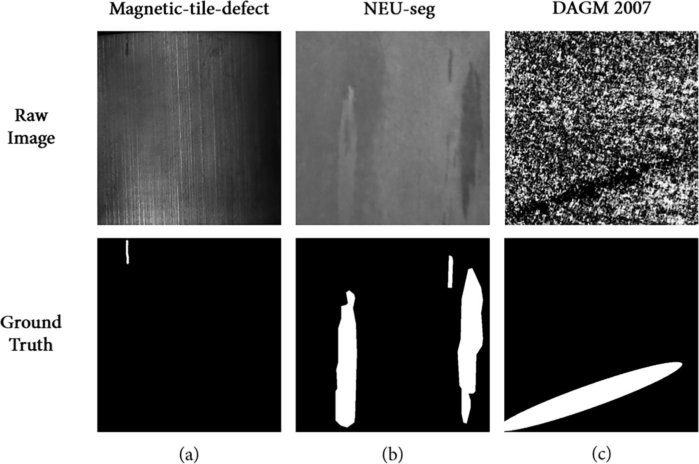
Figure 15: Sample images from the three public industrial datasets used for generalizability verification: (a) Magnetic-tile-defect, (b) NEU-seg, and (c) DAGM 2007
As summarized in Table 12, the proposed method consistently improves segmentation metrics (mAP(mask)) across all three datasets while maintaining comparable box-level performance. Specifically, on the Magnetic-tile-defect dataset, mAP(mask)@50 increased from 79.8% to 84.3%. Similarly, on NEU-seg, the model improved mAP(mask)@50 from 84.9% to 87.2% and mAP(mask)@50:95 from 50.8% to 51.4%. For the DAGM 2007 dataset, while box detection remained comparable, the model achieved a clear gain in the stricter segmentation metric of mAP(mask)@50:95 (55.9% vs. 53.1%). Furthermore, the model maintains exceptional efficiency (e.g., 248.06 FPS on NEU-seg), confirming its robustness and suitability for real-time inspection in diverse industrial environments.
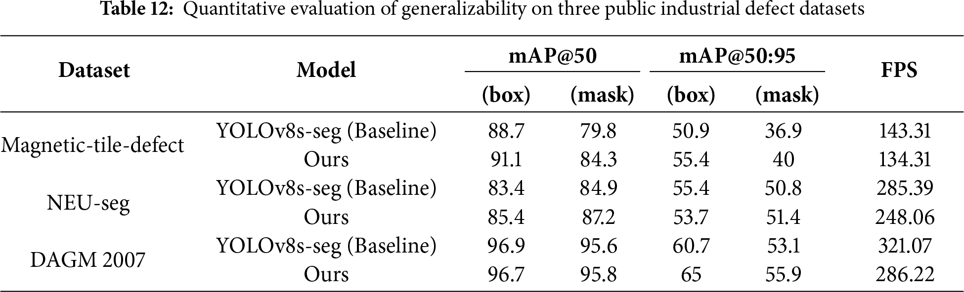
In terms of efficiency, although the integration of the BiFPN and EMA modules introduced a slight computational overhead, the model maintained exceptional inference speeds. For instance, on the NEU-seg dataset, the model achieved 248.06 FPS, remaining well above the requirements for real-time inspection. Collectively, these results confirm that the proposed framework is not limited to a specific dataset but possesses strong generalizability, making it highly effective for various industrial inspection tasks involving complex background textures.
This study developed a framework for detecting surface defects on SiC wafers by integrating an improved YOLOv8-seg instance segmentation model with an improved WGAN-GP data augmentation model. Compared with the original YOLOv8s-seg model, the improved YOLOv8-seg model achieved 3.31% and 5.08% higher mAP(box) and mAP(mask) values, respectively. The mAP(box) and mAP(mask) values increased from 82.9% and 79.3%, respectively, for the original model to 86.21% and 84.38%, respectively, for the improved model. Furthermore, the proposed framework (improved YOLOv8-seg model + improved WGAN-GP model) exhibited mAP(box) and mAP(mask) values of 87.0% and 86.6%, respectively. These values were 4.1% and 7.3% higher, respectively, than those of the original YOLOv8s-seg model. These improvements substantially reduced false positives and missed detections, which are common problems observed in conventional machine vision systems. The proposed WGAN-GP model, in which the original WGAN-GP model is combined with an online data augmentation module, enabled the syntheses of high-quality defect samples even under complex backgrounds. Compared with the original WGAN-GP model, the proposed WGAN-GP model exhibited a 32.2% smaller FID value (84.32 vs. 124.39) and a 29.8% smaller MS-SSIM value (0.141 vs. 0.201). These results confirmed the high fidelity and effectiveness of the proposed generation framework. In summary, the framework developed in this study enhances accuracy and stability in the detection of surface defects on SiC wafers, serving as a viable solution when limited training data are available. This framework also has strong potential for application in other high-precision inspection tasks.
Acknowledgement: Not applicable.
Funding Statement: This research was funded by the National Science and Technology Council (NSTC), Taiwan, grant number NSTC 114-2218-E-167-001.
Author Contributions: The authors confirm contribution to the paper as follows: conceptualization, Chih-Yung Huang; methodology, Chih-Yung Huang and Hong-Ru Shi; software, Hong-Ru Shi; validation, Hong-Ru Shi and Min-Yan Xie; data curation, Hong-Ru Shi; writing—original draft preparation, Chih-Yung Huang and Hong-Ru Shi; writing—review and editing, Chih-Yung Huang and Min-Yan Xie; visualization, Hong-Ru Shi and Min-Yan Xie; supervision, Chih-Yung Huang. All authors reviewed and approved the final version of the manuscript.
Availability of Data and Materials: The SiC wafer defect dataset was collected in-house and is not publicly available due to sensitive manufacturing context and ongoing research/IP considerations. Public datasets used for generalizability verification (Magnetic-tile-defect, NEU-seg, DAGM 2007) are available from their respective sources; trained weights and key implementation details may be provided by the corresponding author upon reasonable request for non-commercial research use.
Ethics Approval: Not applicable.
Conflicts of Interest: The authors declare no conflicts of interest.
References
1. Liu YC, Chen WJ, Qi X, Shen Y, Gu L, Ma HP. Overview of silicon carbide wafer defect types and inspection techniques. In: Proceedings of the 2024 21st China International Forum on Solid State Lighting & 2024 10th International Forum on Wide Bandgap Semiconductors (SSLCHINA: IFWS); 2024 Nov 18–21; Suzhou, China. p. 44–8. [Google Scholar]
2. Goodfellow I, Pouget-Abadie J, Mirza M, Xu B, Warde-Farley D, Ozair S, et al. Generative adversarial networks. arXiv:1406.2661. 2014. [Google Scholar]
3. He K, Gkioxari G, Dollár P, Girshick R. Mask R-CNN. arXiv:1703.06870. 2017. [Google Scholar]
4. Liu S, Qi L, Qin H, Shi J, Jia J. Path aggregation network for instance segmentation. arXiv:1803.01534. 2018. [Google Scholar]
5. Kirillov A, Wu Y, He K, Girshick R. PointRend: image segmentation as rendering. arXiv:1912.08193. 2019. [Google Scholar]
6. Redmon J, Divvala S, Girshick R, Farhadi A. You only look once: unified, real-time object detection. arXiv:1506.02640. 2015. [Google Scholar]
7. Bolya D, Zhou C, Xiao F, Lee YJ. YOLACT: real-time instance segmentation. arXiv:1904.02689. 2019. [Google Scholar]
8. He J, Li T, Wang Z, Cao J, Chen L, Lian Y, et al. Detection and segmentation of overhead transmission line icing conductor based on improved YOLOv5. In: Proceedings of the 2023 3rd International Conference on New Energy and Power Engineering (ICNEPE); 2023 Nov 24–26; Huzhou, China. p. 917–20. [Google Scholar]
9. Sharma D, Indu S, Jayanthi N. Lane-line segmentation using YOLOv7. In: Proceedings of the 2023 2nd International Conference on Vision towards Emerging Trends in Communication and Networking Technologies (ViTECoN); 2023 May 5–6; Vellore, India. p. 1–4. [Google Scholar]
10. Ferguson M, Ak R, Lee YT, Law KH. Detection and segmentation of manufacturing defects with convolutional neural networks and transfer learning. arXiv:1808.02518. 2018. [Google Scholar]
11. Fondevik SK, Stahl A, Transeth AA, Knudsen OO. Image segmentation of corrosion damages in industrial inspections. In: Proceedings of the 2020 IEEE 32nd International Conference on Tools with Artificial Intelligence (ICTAI); 2020 Nov 9–11; Baltimore, MD, USA. p. 787–92. [Google Scholar]
12. Prathyuksha Nair J, Thangakumar J. Revolutionizing leather quality assurance through deep learning powered precision in defect detection and segmentation by a comparative analysis of Mask RCNN and YOLO v8. In: Proceedings of the 2024 International Conference on Advances in Data Engineering and Intelligent Computing Systems (ADICS); 2024 Apr 18–19; Chennai, India. p. 1–6. [Google Scholar]
13. You C, Kong H. Improved steel surface defect detection algorithm based on YOLOv8. IEEE Access. 2024;12(1):99570–7. doi:10.1109/ACCESS.2024.3429555. [Google Scholar] [CrossRef]
14. Tang W, Deng Y, Luo X. RST-YOLOv8: an improved chip surface defect detection model based on YOLOv8. Sensors. 2025;25(13):3859. doi:10.3390/s25133859. [Google Scholar] [PubMed] [CrossRef]
15. Xu A, Li Y, Xie H, Yang R, Li J, Wang J. Optimization and validation of wafer surface defect detection algorithm based on RT-DETR. IEEE Access. 2025;13(1):39727–37. doi:10.1109/ACCESS.2025.3543525. [Google Scholar] [CrossRef]
16. Robinson I, Robicheaux P, Popov M, Ramanan D, Peri N. RF-DETR: neural architecture search for real-time detection transformers. arXiv:2511.09554. 2025. [Google Scholar]
17. Radford A, Metz L, Chintala S. Unsupervised representation learning with deep convolutional generative adversarial networks. arXiv:1511.06434. 2015. [Google Scholar]
18. Arjovsky M, Chintala S, Bottou L. Wasserstein GAN. arXiv:1701.07875. 2017. [Google Scholar]
19. Gulrajani I, Ahmed F, Arjovsky M, Dumoulin V, Courville A. Improved training of Wasserstein GANs. arXiv:1704.00028. 2017. [Google Scholar]
20. Chen SH, Kang CH, Perng DB. Detecting and measuring defects in wafer die using GAN and YOLOv3. Appl Sci. 2020;10(23):8725. doi:10.3390/app10238725. [Google Scholar] [CrossRef]
21. Demirci MY, Beşli N, Gümüşçü A. An improved hybrid solar cell defect detection approach using generative adversarial networks and weighted classification. Expert Syst Appl. 2024;252(2):124230. doi:10.1016/j.eswa.2024.124230. [Google Scholar] [CrossRef]
22. Dewi C, Chen RC, Liu YT, Jiang X, Hartomo KD. Yolo V4 for advanced traffic sign recognition with synthetic training data generated by various GAN. IEEE Access. 2021;9:97228–42. doi:10.1109/ACCESS.2021.3094201. [Google Scholar] [CrossRef]
23. An J, Yang L, Zhou Y. Few-shot catenary pipe cap defect detection based on WGAN-GP and cascading network. In: Proceedings of the 2022 IEEE 10th International Conference on Computer Science and Network Technology (ICCSNT); 2022 Oct 22–23; Dalian, China. p. 24–8. [Google Scholar]
24. Li L, Wang P, Ren J, Lü Z, Li X, Gao H, et al. Synthetic data augmentation for high-resolution X-ray welding defect detection and classification based on a small number of real samples. Eng Appl Artif Intell. 2024;133(4):108379. doi:10.1016/j.engappai.2024.108379. [Google Scholar] [CrossRef]
25. Qiu X, Liu Y, Jin Q, Chen Y, Zhuo C, Sun Q. A diffusion-based approach to wafer defect image generation in semiconductor manufacturing. In: Proceedings of the 2025 Conference of Science and Technology of Integrated Circuits (CSTIC); 2025 Mar 24–25; Shanghai, China. p. 1–3. [Google Scholar]
26. Leiñena J, Saiz FA, Barandiaran I. Latent diffusion models to enhance the performance of visual defect segmentation networks in steel surface inspection. Sensors. 2024;24(18):6016. doi:10.3390/s24186016. [Google Scholar] [PubMed] [CrossRef]
27. Hu Z, Schlosser T, Friedrich M, Silva ALVE, Beuth F, Kowerko D. Utilizing generative adversarial networks for image data augmentation and classification of semiconductor wafer dicing induced defects. arXiv:2407.20268. 2024. [Google Scholar]
28. Jeganathan B. Transformer-based and generative AI framework for automated defect detection in semiconductor wafer inspection. Curr J Appl Sci Technol. 2025;44(11):75–85. doi:10.9734/cjast/2025/v44i114633. [Google Scholar] [CrossRef]
29. Ouyang D, He S, Zhang G, Luo M, Guo H, Zhan J, et al. Efficient multi-scale attention module with cross-spatial learning. In: Proceedings of the ICASSP 2023—2023 IEEE International Conference on Acoustics, Speech and Signal Processing (ICASSP); 2023 Jun 4–10; Rhodes Island, Greece. p. 1–5. [Google Scholar]
30. Tan M, Pang R, Le QV. EfficientDet: scalable and efficient object detection. arXiv:1911.09070. 2019. [Google Scholar]
31. Heusel M, Ramsauer H, Unterthiner T, Nessler B, Hochreiter S. GANs trained by a two time-scale update rule converge to a local Nash equilibrium. arXiv:1706.08500. 2017. [Google Scholar]
32. Nasr MA, AlRahmawy MF, Tolba AS. Multi-scale structural similarity index for motion detection. J King Saud Univ Comput Inf Sci. 2017;29(3):399–409. doi:10.1016/j.jksuci.2016.02.004. [Google Scholar] [CrossRef]
33. Bolya D, Foley S, Hays J, Hoffman J. TIDE: a general toolbox for identifying object detection errors. arXiv:2008.08115. 2020. [Google Scholar]
34. Zhang Q, Chen M, Shen B, Guo B, Chen D, Huang Y, et al. Optical plasma boundary detection using improved YOLOv8 segmentation network on EAST tokamak. Nucl Eng Technol. 2025;57(6):103411. doi:10.1016/j.net.2024.103411. [Google Scholar] [CrossRef]
35. Bai R, Wang M, Zhang Z, Lu J, Shen F. Automated construction site monitoring based on improved YOLOv8-seg instance segmentation algorithm. IEEE Access. 2023;11(5):139082–96. doi:10.1109/ACCESS.2023.3340895. [Google Scholar] [CrossRef]
36. Wang CY, Yeh IH, Liao HM. YOLOv9: learning what you want to learn using programmable gradient information. arXiv:2402.13616. 2024. [Google Scholar]
37. Wang X, Zhang R, Kong T, Li L, Shen C. SOLOv2: dynamic and fast instance segmentation. arXiv:2003.10152. 2020. [Google Scholar]
38. Cheng B, Misra I, Schwing AG, Kirillov A, Girdhar R. Masked-attention mask transformer for universal image segmentation. In: Proceedings of the 2022 IEEE/CVF Conference on Computer Vision and Pattern Recognition (CVPR); 2022 Jun 18–24; New Orleans, LA, USA. p. 1280–9. [Google Scholar]
39. Huang Y, Qiu C, Guo Y, Wang X, Yuan K. Surface defect saliency of magnetic tile. In: Proceedings of the 2018 IEEE 14th International Conference on Automation Science and Engineering (CASE); 2018 Aug 20–24; Munich, Germany. p. 612–7. [Google Scholar]
40. Dong H, Song K, He Y, Xu J, Yan Y, Meng Q. PGA-Net: pyramid feature fusion and global context attention network for automated surface defect detection. IEEE Trans Ind Inform. 2020;16(12):7448–58. doi:10.1109/TII.2019.2958826. [Google Scholar] [CrossRef]
41. Matthias W, Tobias H, Fred H. Weakly supervised learning for industrial optical inspection. In: Proceedings of the 29th Annual Symposium of the German Association for Pattern Recognition (DAGM 2007); 2007 Sep 12–14; Heidelberg, Germany. [Google Scholar]
Cite This Article
 Copyright © 2026 The Author(s). Published by Tech Science Press.
This work is licensed under a Creative Commons Attribution 4.0 International License , which permits unrestricted use, distribution, and reproduction in any medium, provided the original work is properly cited.
 Downloads
 Citation Tools