
 Submit a Paper
 Propose a Special lssue
 Open Access
ARTICLE

Impact of Window Layers on Selenium Distribution and Photovoltaic Performance in CdSexTe1−x/CdTe Solar Cells
1 College of Materials Science and Engineering & Institute of New Energy and Low-carbon Technology, Sichuan University, Chengdu, 610065, China
2 Engineering Research Center of Alterative Energy Materials & Devices, Ministry of Education, Chengdu, 610065, China
* Corresponding Author: Lili Wu. Email:
Chalcogenide Letters 2026, 23(1), 2 https://doi.org/10.32604/cl.2026.076362
Received 19 November 2025; Accepted 26 December 2025; Issue published 26 January 2026
 View Full Text
 Download PDF
Abstract
The incorporation of the Se element in CdTe solar cells is critical, while the low bandgap CdSexTe1−x, formed by the interdiffusion of CdTe and CdSe during device preparation, can promote the carrier lifetime. Different window layers formed by CdSe w/o MZO or CdS have different Se distributions. This paper systematically evaluates the influence of four types of window layers (CdSe, CdS/CdSe, MZO/CdSe and MZO/CdS/CdSe) on the performance of CdTe solar cells, and focuses on the correlation between the window layers and the Se distribution characteristic, carrier recombination mechanism, and device efficiency. The results show that CdSe and MZO/CdS/CdSe window layer devices achieve Eff of 15.21% and 14.40%, respectively. The CdSe and MZO/CdS/CdSe devices exhibit relatively high Ea of 1.41 eV and 1.39 eV from J-V-T measurements, coupled with high Rrec of 9458 Ω and 8293 Ω, respectively. This indicates suppressed recombination, suggesting that non-radiative recombination is reduced. In contrast, the CdS/CdSe and MZO/CdSe devices show lower performance. Their extrapolated Ea values are 1.25 eV and 1.31 eV, with correspondingly lower Rrec values of 2207 Ω and 3304 Ω. These results point to faster recombination rates and an increased proportion of non-radiative recombination, consistent with their suboptimal Eff. Detailed analysis of Se distribution reveals that S-Se interdiffusion in S-containing devices results in the x-value decrease (highest value of Se content in CdSexTe1−x), thereby suppressing the long-wavelength expansion. In devices of S-free window layers, the formed CdSexTe1−x alloy has a relatively higher x-value, allowing the long-wavelength response to extend beyond 850 nm. It can be concluded that CdSe is the optimal window layer for CdTe Solar Cells, which can both form a desirable Se distribution and a good junction with less interface recombination.Keywords
Supplementary Material
Supplementary Material FileCdTe thin-film solar cells, as commercialized polycrystalline thin-film photovoltaic devices, dominate over 90% of the thin-film photovoltaic market, with the highest reported efficiency reaching 23.08% [1,2]. The window layer is the essential part of the CdTe solar cell, enhancing transmittance and facilitating carrier separation through heterojunction formation. CdS has been the typical window layer for CdTe solar cells since the 1980s, owing to the favorable lattice match and stable heterojunction achieved by forming a CdSxTe1−x alloy [3,4]. However, the bandgap of CdS is ~2.4 eV, leading to significant parasitic absorption of photons at wavelengths less than 520 nm, which limits the short-circuit current density (JSC) [5,6]. In the early 2000s, Mg-doped ZnO (MZO) emerged as an alternative window layer material, characterized by a doping-tunable bandgap (3.4–4.0 eV) and high transparency [7,8]. Its carrier mobility can be further improved through annealing processes [9,10]. Subsequent studies revealed that using CdSe as a window layer leads to the formation of a CdSexTe1−x alloy with CdTe [11,12]. This alloy effectively reduces the bandgap, extends the spectral response into the near-infrared region, and increases the carrier concentration, making it a promising window layer candidate [13,14,15].
The Se diffusion from CdSe to form a CdSexTe1−x layer has attracted significant interest. The Calculated results demonstrate that the lattice constant of the CdSexTe1−x alloy layer is between that of CdSe (6.05 Å) and CdTe (6.48 Å) [16], which can alleviate the lattice mismatch at the heterojunction interface. Besides, the formed CdSexTe1−x alloy has a lower bandgap, which enhances long-wavelength photon collection, thus effectively boosting the JSC [17,18]. Studies have shown that Se preferentially segregates at CdTe grain boundaries, exhibiting beneficial passivation effects [19,20], and the optical properties of the CdSexTe1−x alloy are influenced by the Se content [21]. Furthermore, CdSexTe1−x films are known to enhance carrier lifetimes [22,23]. In particular, films with a graded Se concentration profile exhibit superior lifetimes compared to uniformly alloyed layers, owing to optimized band alignment and reduced recombination [24,25].
The Se content and diffusion in CdSexTe1−x/CdTe solar cell critically affects device performance. But how the window layer influences Se behavior remains unclear. This work fabricates CdTe solar cells with four window layers (CdSe, CdS/CdSe, MZO/CdSe, MZO/CdS/CdSe) and systematically compares their device performance, pn junction characteristics, and carrier recombination method. Innovatively, cross-sectional elemental analysis was used to reveal the distinct Se distribution induced by each window layer, thereby explaining the differences in device performance from the perspective of Se diffusion. These findings provide insights that could supply the design of optimal window layers in CdTe solar cells.
CdTe solar cells with four window layers were fabricated using a conventional superstrate structure. The window layer structures, illustrated in Fig. 1, correspond to CdSe, CdS/CdSe, MZO/CdSe, and MZO/CdS/CdSe, respectively. Commercially purchased TEC12 FTO glass was used as the substrate. They were ultrasonically cleaned in a 1:10 (v/v) detergent/DI-water solution for 35 min. Subsequently, the substrates were soaked in DI-water and underwent ultrasonic agitation for three 20-min cycles to ensure the removal of organic residues. The substrates were boiled in DI-water for 10 min, cooled, and dried in an oven. The window layers were deposited by magnetron sputtering. For all devices, a consistent thickness was maintained for each layer: 20 nm for CdS, 70 nm for MZO, and 120 nm for CdSe. The MZO layer was sputtered at room temperature using a ZMO target (MgO: ZnO = 23:79 mol%) under an Ar/O2 atmosphere (39.5:0.5 sccm). CdS and CdSe layers were deposited in pure Ar using 99.99% purity targets. For multilayer configurations (MZO/CdSe, CdS/CdSe, MZO/CdS/CdSe), sequential sputtering was performed without breaking the vacuum. CdTe absorber layers with thicknesses of 3–4 μm were deposited via closed-space sublimation (CSS) using Cu-doped CdTe materials under ~4 KPa He/Ar (50:100) gas mixture with source/substrate temperatures of 680/600°C, respectively. Post-deposition, CdCl2 treatment was applied by ultrasonic spraying of 0.1 mol/L CdCl2 solution onto the CdTe surface at 200°C (three cycles, 5 min each), followed by annealing at 395°C for 35 min in N2, which has been demonstrated to be the optimal parameters in our previous experiments. The CdTe was etched using bromine-methanol solution, followed by deposition of an 80 nm Au via vacuum evaporation to form the back electrode. Laser scribing defined individual devices with an area of 0.24 cm2. Since this study focuses primarily on the influence of different window layer structures on device performance and Se distribution, the adopted fabrication process can effectively minimize the back contact barrier and does not interfere with the experimental conclusions. For each window layer, 24 devices were fabricated, and after statistical analysis of their performance, representative devices were selected for further characterization.
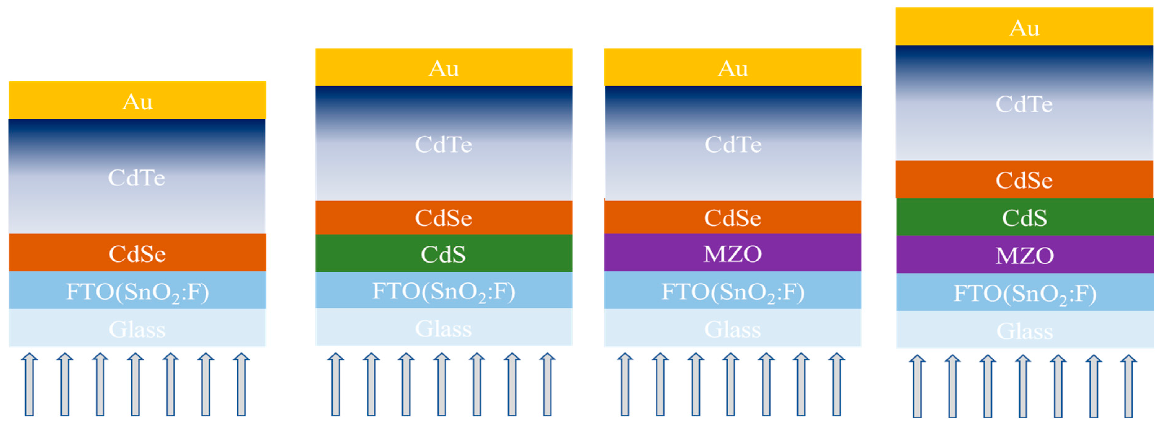
Figure 1: Schematic of four CdTe solar cell with different window layers in a superstrate structure. The arrow indicates the direction of light incidence.
2.2 Film and Device Characterization
The current density-voltage (J-V) characteristics of CdTe devices were measured under simulated AM1.5G illumination (100 mW/cm2) at room temperature using a Keithley 2400-LV source meter coupled with an ABET Technologies Sun 3000 solar simulator. The light intensity was calibrated using a GaAs reference cell (PV Measurements). External quantum efficiency (EQE) spectra were acquired across 300–950 nm wavelengths via a quantum efficiency measurement system (QEX10, PV Measurements). Dark current density-voltage (Dark J-V) curves were recorded at a stable ambient temperature of 25°C ± 1°C using an Agilent 4284A precision LCR meter. Temperature-dependent current density-voltage (J-V-T) measurements in the 298–338 K range were performed under illumination using a custom-designed resistive heater stage integrated with dual temperature sensors. The electrochemical impedance spectroscopy (EIS) measurements were performed using an IviumStat.h electrochemical workstation equipped with simulated solar illumination at an intensity of 100 mW/cm2. The measurements were performed under a forward bias of 0.5 V, with a frequency range from 100,000 Hz to 0.1 Hz. Cross-sectional scanning electron microscopy (SEM) images and elemental distribution profiles were obtained using a ZEISS Gemini SEM 300 scanning electron microscope equipped with an Oxford Xplore energy-dispersive X-ray spectroscopy (EDS) system. To avoid contamination, all sample cross-sections were tested immediately after liquid nitrogen fracturing. All cross-section were measured under identical conditions with an accelerating voltage of 15 kV, a beam current of 0.5 nA, a sample tilt of 0°, and a 100 s acquisition time per line-scan, to obtain a high signal-to-noise ratio and statistical reliability.
3.1 J-V Characteristics and EQE
Statistical analysis of the device is presented in Fig. 2a–d, where the mean values of Eff, VOC, JSC, and FF are labeled below the box plots. Among the four structures, CdSe devices exhibited the highest average Eff of 14.39%, primarily attributed to superior JSC (28.05 mA/cm2) and FF (67%). The MZO/CdS/CdSe devices achieved an average Eff of 13.30%, driven by its highest VOC (779 mV) due to effective interface recombination suppression. In contrast, MZO/CdSe devices showed the lower average Eff (10.73%), linked to their poorest FF (53.41%). CdS/CdSe devices demonstrated the lowest average Eff (9.06%), resulting from suboptimal JSC and VOC values. The correlation between device performance and carrier recombination mechanisms will be analyzed in Section 3.2.
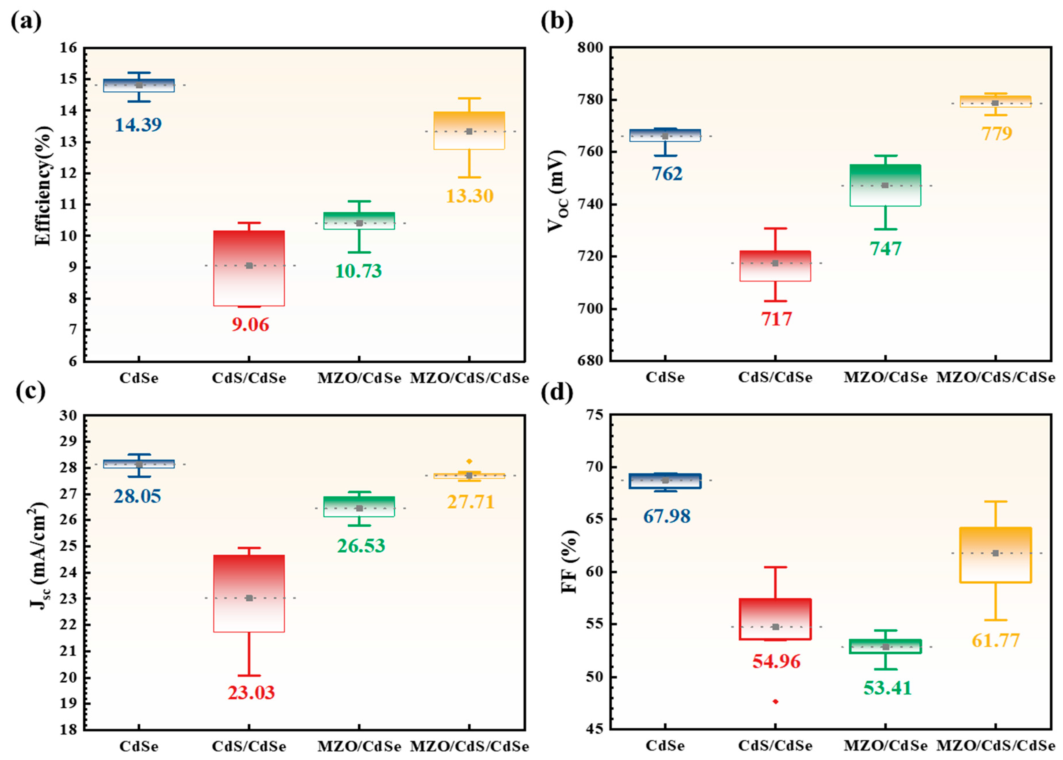
Figure 2: Box plots of photovoltaic performance parameters for CdTe solar cells with different window layers: (a) Efficiency (Eff), (b) Open-circuit voltage (VOC), (c) Short-circuit current density (JSC), (d) Fill factor (FF). The mean values of each parameter are labeled below the corresponding box plots.
Fig. 3a displays the J-V curves of the highest-efficiency devices for each window layer, while Fig. 3b presents the EQE spectra and corresponding integrated current densities for the four devices. A comparison between the measured current density (Jmeasure) and the integrated current density (Jintegrate) are summarized in Table S1. As shown in Fig. 3b, the EQE spectra show no discernible parasitic absorption of CdSe, indicating complete interdiffusion of CdSe and CdTe in all samples [15]. The CdSe device exhibits the highest spectral response, achieving an integrated current density of 27.37 mA/cm2, followed by MZO/CdS/CdSe (26.71 mA/cm2) and MZO/CdSe (26.39 mA/cm2), with the CdS/CdSe performing the worst (24.17 mA/cm2). Notably, in the 850–900 nm range as shown in Fig. 3c, the EQE values of CdSe, CdS/CdSe, and MZO/CdSe devices significantly surpass those of the MZO/CdS/CdSe device. This discrepancy is likely attributed to variations in Se content and distribution profiles, which will be further analyzed in Section 3.3.
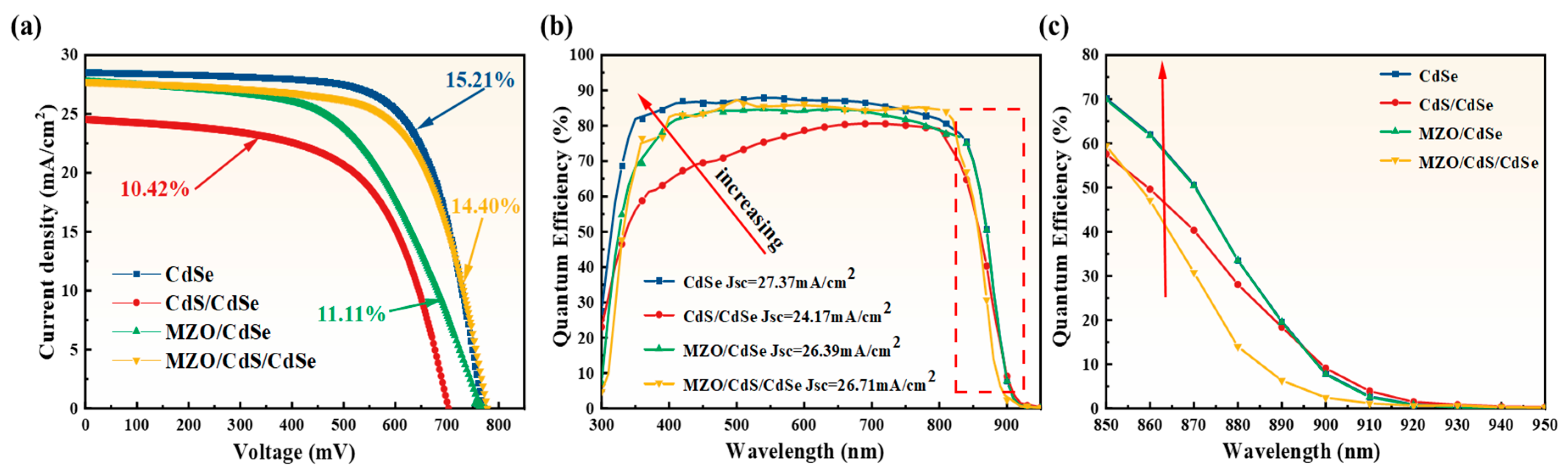
Figure 3: CdTe solar cells with different window layers. (a) J-V curves of the highest efficiency, (b) EQE spectra across 300–950 nm wavelength (integrated JSC labeled for each device), and (c) EQE profiles in the 850–950 nm wavelength range.
3.2 Carrier Recombination Mechanism and pn Junction Characteristic
To investigate the carrier recombination mechanisms in devices with different window layers, J-V-T measurements were performed. Based on the J-V characteristic Eq. (1) and the diode current relation Eq. (2), the J-V-T relationship was derived. When J = 0, the temperature-dependent open-circuit voltage (VOC-T) relationship was obtained in Eq. (3) [26,27].
Since different window layers form CdSexTe1−x alloy with distinct bandgap, Fig. 4a–d presents the device bandgap values Eip g for CdSe, CdS/CdSe, MZO/CdSe, and MZO/CdS/CdSe window layer devices determined through the inflection points of the EQE spectra [29,30]. The calculated values are 1.409 eV, 1.417 eV, 1.409 eV, and 1.425 eV, respectively, enabling comparative analysis between device bandgaps and Ea to elucidate the recombination mechanisms in devices with different window layer structures.
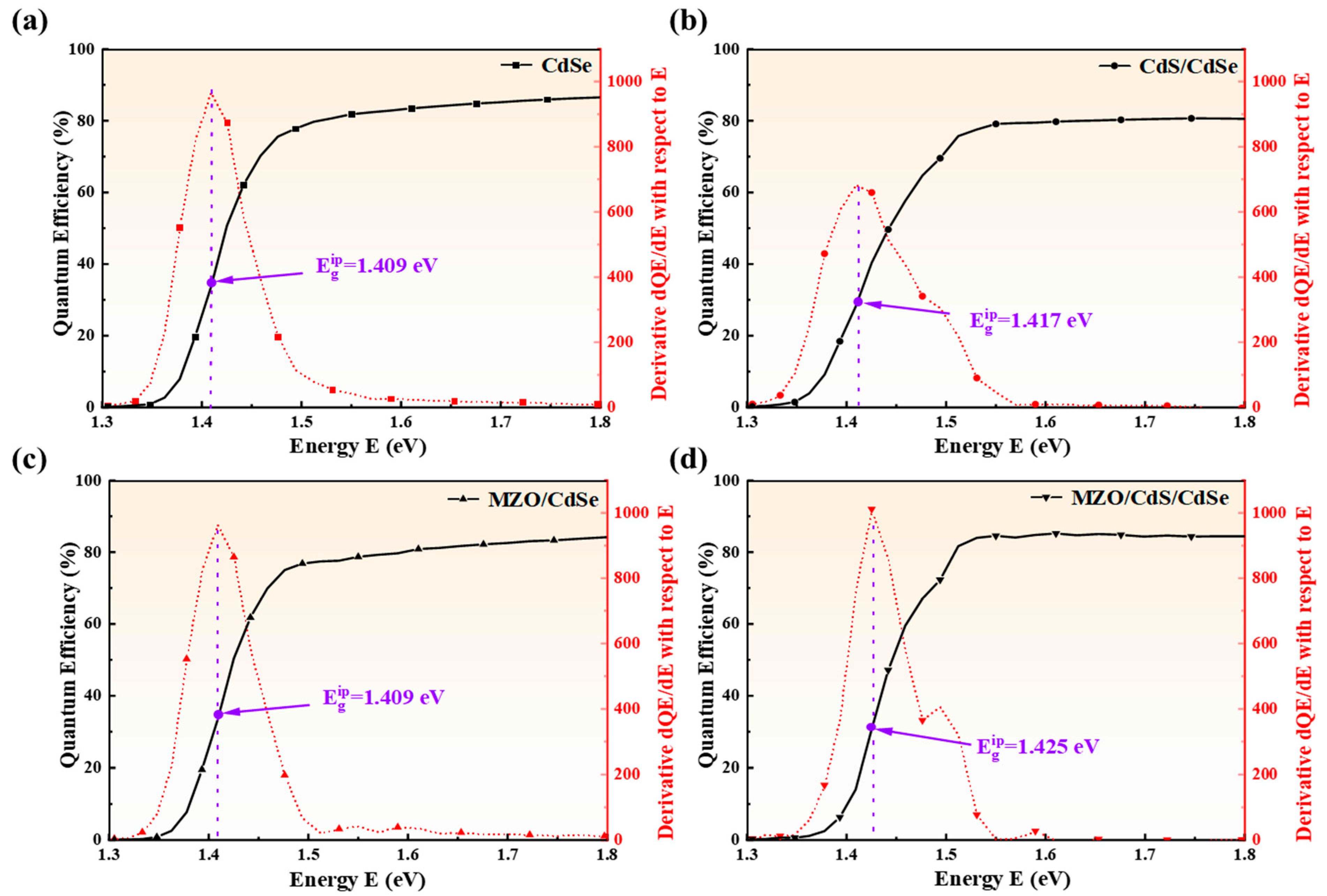
Figure 4: The bandgap determined by differentiation of the EQE spectra for (a) CdSe, (b) CdS/CdSe, (c) MZO/CdSe, and (d) MZO/CdS/CdSe.
According to Fig. 5a,b, J-V curve measurements were performed from 293.5 K to 338.5 K with 5 temperature increments. Fig. 5a reveals a continuous reduction in bandgap and a linear dependence of VOC on temperature as temperature increases. J-V-T curves for the different window layer devices are provided in Fig. S1. As the temperature increases, the VOC of all devices decreases steadily, while a slight rise in the JSC is observed. Fig. 5b presents the extrapolated VOC-T curves at 0 K. The linear fitting results of the VOC-T are summarized in Table S2. The fitted slopes show very small standard errors, indicating high precision in the Ea. Furthermore, the obtained R2 values all exceed 0.99, confirming a good linear relationship. This strong linearity suggests that a single recombination mechanism dominates and that the contribution of the back contact to the measured Ea is negligible.
Ea and average VOC values of four devices summarized in Table 1. The MZO/CdS/CdSe and CdSe window layers show Ea of 1.41 eV and 1.39 eV, with voltage losses of 0.015 eV and 0.019 eV relative to their Egip of 1.425 eV and 1.409 eV, respectively. Their average VOC values are 779 mV and 762 mV, consistent with the Ea trend and suggesting lower non-radiative recombination. In contrast, The MZO/CdSe and CdS/CdSe window layers exhibit Ea of 1.31 eV and 1.25 eV, corresponding to voltage losses of 0.099 eV and 0.167 eV relative to their Egip of 1.409 eV and 1.417 eV. Their average Voc values are 747 mV and 717 mV are consistent with this Ea trend, indicating dominant non-radiative recombination.
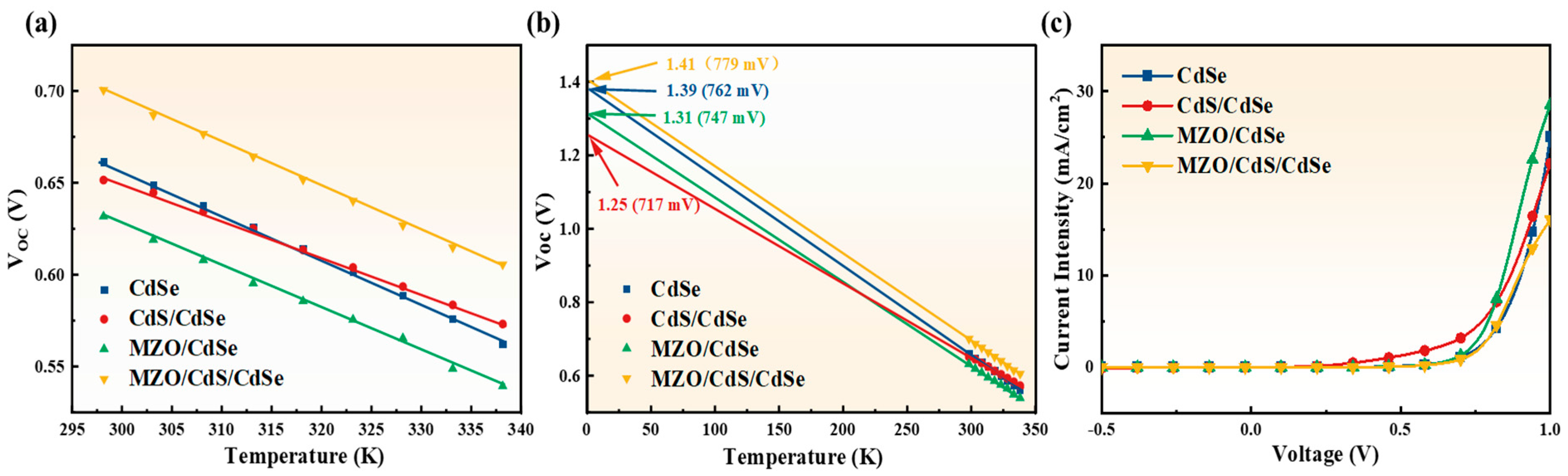
Figure 5: Four window layer devices (a) VOC-T, (b) VOC-T extrapolated to 0 K, and (c) Dark J-V.
Dark J-V curves of the devices are shown in Fig. 5c. The relationship between dark current density and applied bias voltage can be described by Jdark = J0[exp(qV/nkT) − 1], where Jdark is the dark current density, and V is the applied bias. Logarithmic transformation of both sides yields LnJ-V curves. Linear fitting near the zero bias region provided the slope and intercept to determine J0 and n for four devices in Table 1. J0, inversely related to carrier recombination in the space charge region, showed smaller values of 1.4 × 10⁻⁷ and 4.8 × 10⁻⁷ mA/cm2 for MZO/CdS/CdSe and CdSe devices, corresponding to lower recombination and higher VOC. The n for the CdSe and MZO/CdS/CdSe devices is 1.50 and 1.58, respectively, corresponding to diffusion-limited dark current. In contrast, MZO/CdSe and CdS/CdSe devices exhibited larger J0 values 1.9 × 10⁻⁶ and 6.9 × 10⁻⁶ mA/cm2 and higher n values 1.83 and 2.13, indicating recombination-dominated current and inferior diode characteristics [31,32].
Table 1: Ea values and dark J-V characteristic parameters for four window layer devices.
| Window Layer | VOC | Ea | J0 | n |
|---|---|---|---|---|
| (mV) | (eV) | (mA/cm2) | ||
| CdSe | 762 | 1.39 | 4.8 × 10⁻⁷ | 1.58 |
| CdS/CdSe | 717 | 1.25 | 6.9 × 10⁻⁶ | 2.13 |
| MZO/CdSe | 747 | 1.31 | 1.9 × 10⁻⁶ | 1.83 |
| MZO/CdS/CdSe | 779 | 1.41 | 1.4 × 10⁻⁷ | 1.50 |
The series resistance (Rs), charge transfer resistance (Rct) and recombination resistance (Rrec) of these devices were characterized by performing EIS measurements under simulated solar illumination at 100 mW/cm2 (light condition) and complete darkness (dark condition) [33,34]. The resulting Nyquist plots for the different devices, recorded under light/dark conditions, are presented in Fig. 6a,b respectively. In Fig. 6, a semicircle is observed under all test conditions and can be fitted using an equivalent circuit, as shown in the inset. The relevant parameters extracted from fitting the semicircles in the Nyquist plots are summarized in Table 2.
In Fig. 6a, the Rs represents the total internal resistance of the device, which includes contributions from the FTO substrate and the metal electrodes. The Rct denotes the ease of charge transfer across the heterojunction interface. A smaller Rct indicates more efficient charge transport [35]. As summarized in Table 2, the CdSe and MZO/CdS/CdSe devices exhibit relatively low Rs values of 25.6 Ω and 28.8 Ω, respectively. In contrast, the CdS/CdSe and MZO/CdSe devices show higher Rs values of 38.1 Ω and 44.9 Ω. The Rct of the CdSe and MZO/CdS/CdSe devices exhibits lower values of 186.3 Ω and 285.4 Ω, respectively, suggesting higher charge transfer efficiency, which corresponds to their higher Eff. Conversely, the CdS/CdSe and MZO/CdSe devices have significantly larger Rct values of 611.5 Ω and 440.3 Ω, indicating lower charge transfer efficiency and consistent with their lower Eff.
Moreover, the Rrec can be obtained under dark condition in Fig. 5b, and it is related to the recombination at the interface between the window layer and CdTe. A larger Rrec indicates lower recombination rate within the device [36]. As summarized in Table 2, the high Rrec of 9458 Ω and 8293 Ω for CdSe and MZO/CdS/CdSe devices suggests suppressed recombination. In contrast, the CdS/CdSe and MZO/CdSe devices show considerably lower Rrec of 2207 Ω and 3304 Ω, pointing to faster recombination rates. These results are consistent with the findings from the J-V-T measurements.
The constant phase element power exponent (CPE-P) in EIS is generally used to assess interfacial quality and homogeneity, with its value ranging from 0 to 1 [37]. A value closer to 1 suggests a more ideal capacitive behavior and a more homogeneous interface. As listed in Table 2, the CPE-P values for the CdSe and MZO/CdS/CdSe devices are 0.922 and 0.920, respectively, indicating high interfacial uniformity. Conversely, the significantly lower CPE-P values of 0.763 for CdS/CdSe and 0.854 for MZO/CdSe imply the presence of greater interfacial disorder and a higher defect state density. A detailed analysis of the device interfaces will be presented in Section 3.3.
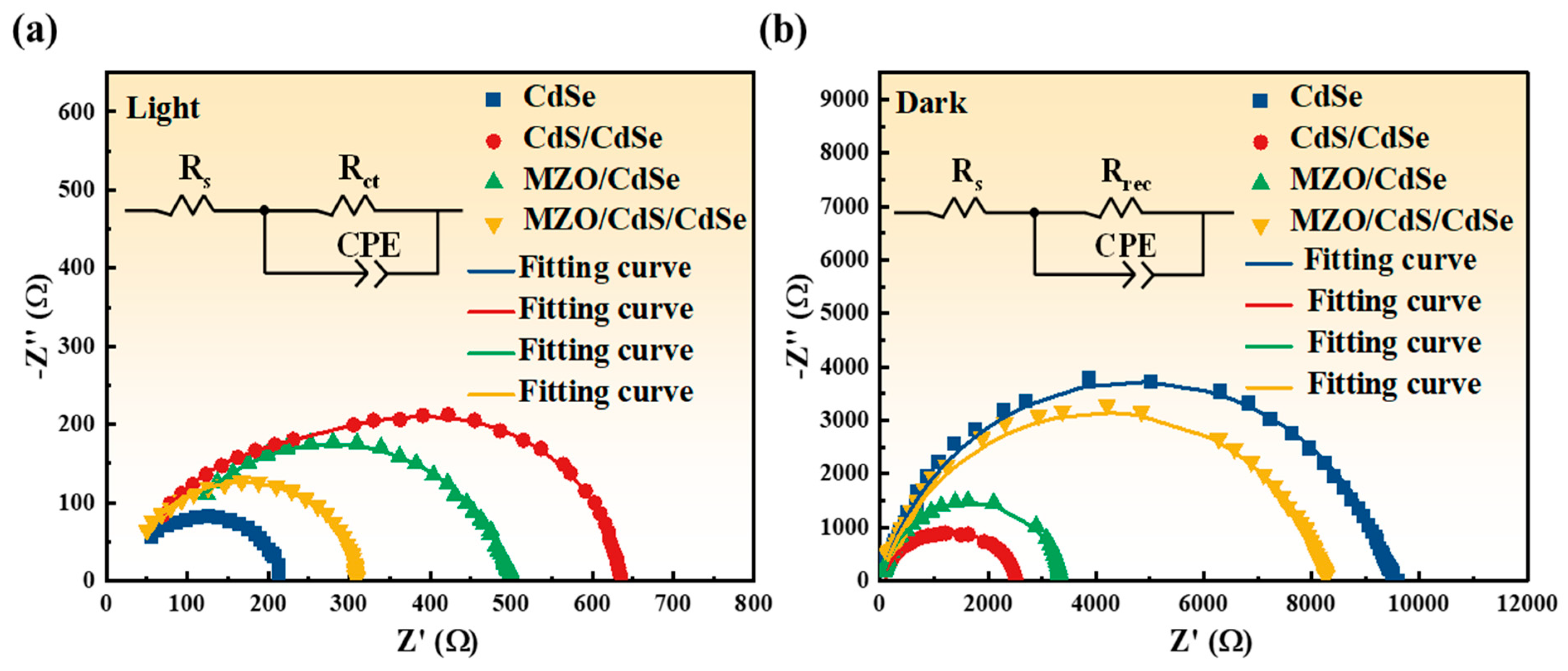
Figure 6: Nyquist plots of CdTe solar cells with the different window layer at (a) light condition and (b) dark condition.
Table 2: Electrochemical parameters extracted from Nyquist plots for different window layer devices.
| Window Layer | Rs | Rct | Rrec | CPE-P |
|---|---|---|---|---|
| Ω | Ω | Ω | ||
| CdSe | 25.6 | 186.3 | 9458 | 0.922 |
| CdS/CdSe | 38.1 | 611.5 | 2207 | 0.763 |
| MZO/CdSe | 44.9 | 440.3 | 3304 | 0.854 |
| MZO/CdS/CdSe | 28.8 | 285.4 | 8293 | 0.920 |
3.3 Cross-Sectional Morphology and Elemental Distribution
As shown in Fig. 7a–d corresponds to the cross-sectional SEM morphology of CdSe, CdS/CdSe, MZO/CdSe, and MZO/CdS/CdSe at 40 K times magnification, respectively. Both the CdSe in Fig. 7a and the MZO/CdS/CdSe devices in Fig. 7d exhibit interfaces free of obvious voids. This indicates that the CdTe film grows with higher density at the interface of these two window layer devices. In contrast, the interface of the CdS/CdSe device in Fig. 7b exhibits numerous voids with an average size of ~500 nm. Additionally, the SEM image of the MZO/CdSe cross-section in Fig. 7c reveals several smaller voids averaging ~100 nm in size. The voids at the interface introduce a large number of interfacial defect states, which will increase the non-radiative recombination of the device and significantly reduce the VOC [38,39]. Generally, interfacial voids formation may stem from the serval mechanisms, including the Kirkendall effect [40,41], the coalescence of gas bubbles during sputtering deposition [42,43,44], and the poor interfacial compatibility during film growth [45,46]. Numerous studies have shown that the CdS/CdSe structure is prone to void formation during CdTe deposition due to interfacial mismatch [47,48]. The interfacial voids observed in the MZO/CdSe device are also likely to originate from the poor mismatch between MZO and CdSe. Furthermore, many studies indicate that the interface between MZO and CdSeTe also tends to form unfavorably [49,50]. In contrast, CdS exhibits superior compatibility with MZO enabling coherent growth, a lower defect density, and consequently a higher Ea in the MZO/CdS/CdSe device [27].
Fig. 7e–h show the depth profiles of Sn, Se, Te, Zn, and S signal intensities, obtained from EDS line-scans across different window layer cross-sections. The profiles trace the signal variation from the glass substrate into the absorber layer, as indicated by the white arrow. For a direct comparison of the elemental distribution across different window layers, the depth scales were aligned by setting the position of the maximum Sn intensity in each device to the zero point of x axis. The resulting normalized Sn distribution profiles are presented in Fig. S2. The reliability of the EDS elemental analysis is evaluated by comparing the measured weight percentage (wt%) against its statistical uncertainty (wt% Sigma). As detailed in Table S3 of the Supplementary Materials, the significant discrepancy between the two values for all elements indicates a high level of confidence in the results.
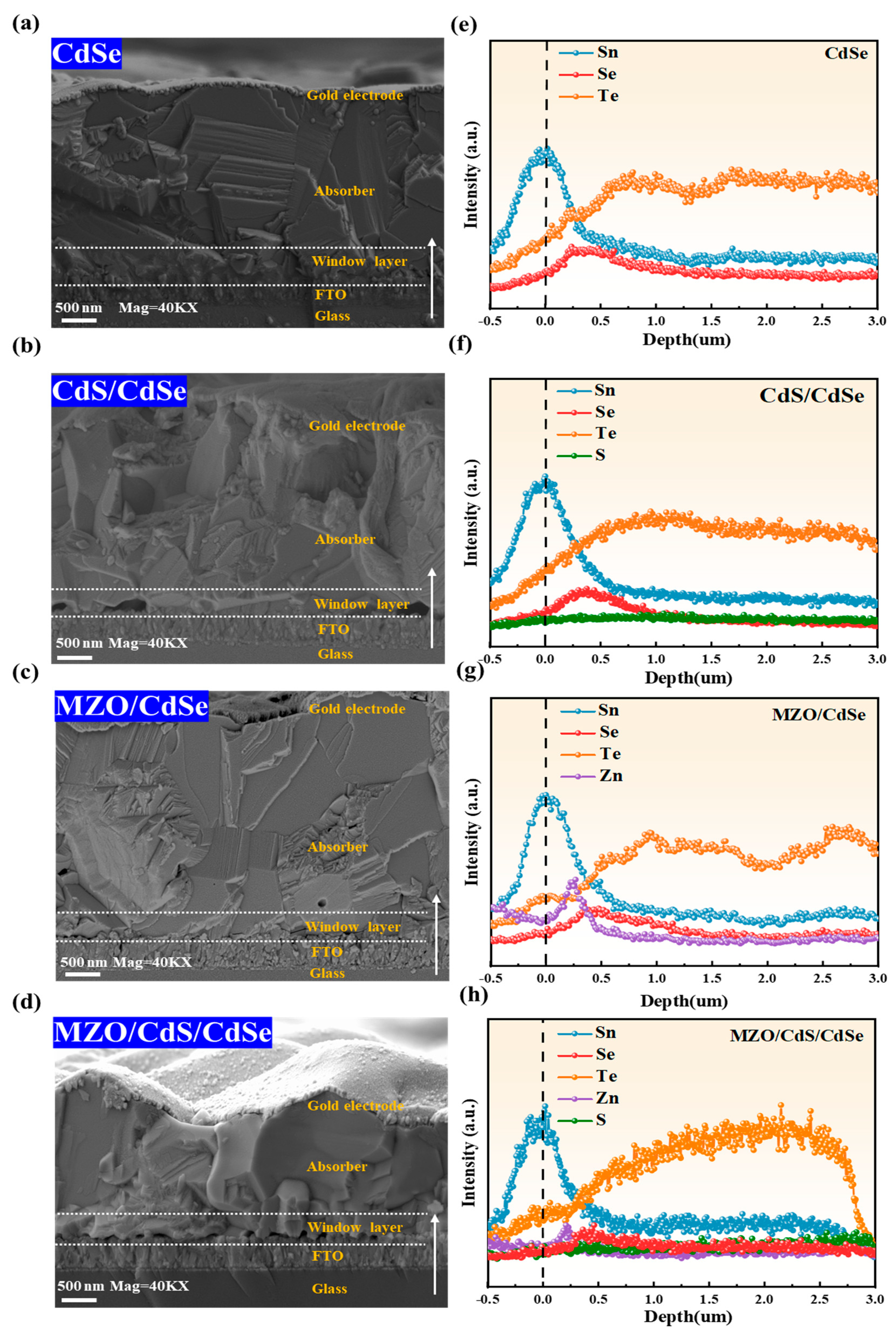
Figure 7: Cross-sectional SEM micrographs of different structures, taken at 40,000× magnification (left) (a) CdSe, (b) CdS/CdSe, (c) MZO/CdSe, and (d) MZO/CdS/CdSe; cross-sectional line-scan elemental distributions of the different structures (right), with the white arrows representing the direction of scanning and the highest value of Sn content as the zero point (e) CdSe, (f) CdS/CdSe, (g) MZO/CdSe, and (h) MZO/CdS/CdSe.
The low atomic number of S and low content from the 20 nm CdS layer cannot the effective detection of its diffusion profile by EDS line-scan in CdS/CdSe and MZO/CdS/CdSe devices. The line-scan elemental profiles of the four devices in Fig. 7e–h show that Se diffuses from the CdSe both forward and backward. Pronounced Te/Se interdiffusion is observed within ~500 nm from the front interface, confirming the formation of CdSexTe1−x. This alloying primarily occurs near the front interface and exhibits an inhomogeneous distribution, which aligns with earlier reports [51]. Zn diffusion was used to monitor the interdiffusion of the MZO layer. As shown in Fig. 7g,h, Zn is confined to within ~200 nm and displays a sharp diffusion profile, indicating that the MZO layer did not undergo significant diffusion. This is further evidenced by the distinct Zn-enriched region at the interface in Fig. 8, consistent with the notable stability of MZO [52,53,54].
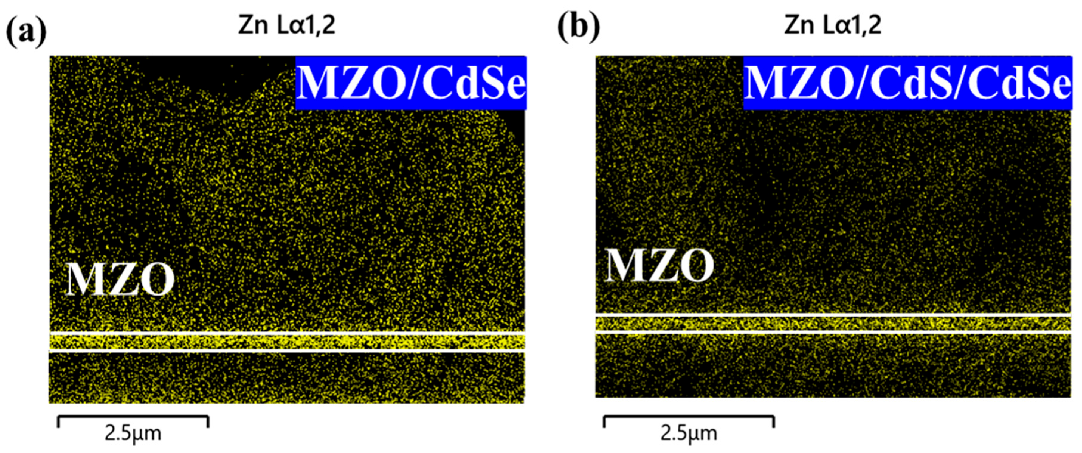
Figure 8: EDS mapping of Zn distribution across device cross-sections. (a) MZO/CdSe and (b) MZO/CdS/CdSe.
Based on the depth profiles of Se and Te in Fig. 7e–h, the Se/(Se + Te) ratio was calculated, with its corresponding x-value (highest value of Se content in CdSexTe1−x) shown in Fig. 9a. The x-value is highest in the CdSe and MZO/CdSe structures (0.35), followed by the CdS/CdSe structure (0.31), and lowest in the MZO/CdS/CdSe structure (0.28). Previous reports indicate that CdSexTe1−x exhibit a bandgap bowing effect, with a minimum bandgap of approximately 1.40 eV when x is around 0.35 [18,55]. The x-value of 0.35 for both CdSe and MZO/CdSe window layers indicates that devices should correspond to the strongest long-wavelength response. A moderate response is expected for CdS/CdSe, while the MZO/CdS/CdSe is likely to show the weakest response. Interestingly, the EQE spectra in Fig. 3c show that the long-wavelength response of the four window layer devices aligns with the above prediction, confirming that the window layer indeed influences the Se content in CdSexTe1−x and the long-wavelength response of the EQE.
Based on the above data, we further analyzed the Se diffusion. Fig. 9b depicts the normalized Se elemental profiles across the different window layer structures. The position corresponding to this maximum is defined as the Se-diffusion center. The Se-diffusion centers are located at 0.24 μm for the CdSe structure and at 0.31 μm for the MZO/CdSe structure. The 0.07 μm difference matches the thickness of the MZO layer, indicating that no significant interdiffusion occurs between MZO and CdSe. This observation aligns with the earlier cross-sectional EDS mapping results of Zn distribution. The Se-diffusion center is located at 0.37 μm in the CdS/CdSe device and at 0.46 μm in the MZO/CdS/CdSe device. A shift of 0.13 μm is observed between the CdS/CdSe structure and the CdSe structure. This shift significantly exceeds the 20 nm thickness of the CdS layer, suggesting pronounced interdiffusion between S and Se [56]. The further shift of 0.09 μm from the CdS/CdSe to the MZO/CdS/CdSe structure is slightly larger than the 70 nm thickness of the MZO layer. These results indicate that in S-containing devices, S-Se interdiffusion can shift the Se-diffusion center toward the absorber bulk, thereby reducing the Se content in the CdSexTe1−x layer. A greater shift correlates with a lower Se content in CdSexTe1−x.
In conclusion, the window layer influences not only the photovoltaic performance, but also the Se distribution and the x-value of the CdSexTe1−x layer when the total Se content is the same. This x-value determines the EQE response and directly impact the JSC. Therefore, the CdSe/CdTe device achieves both an appropriate Se distribution and a superior performance among the four window layer structures.
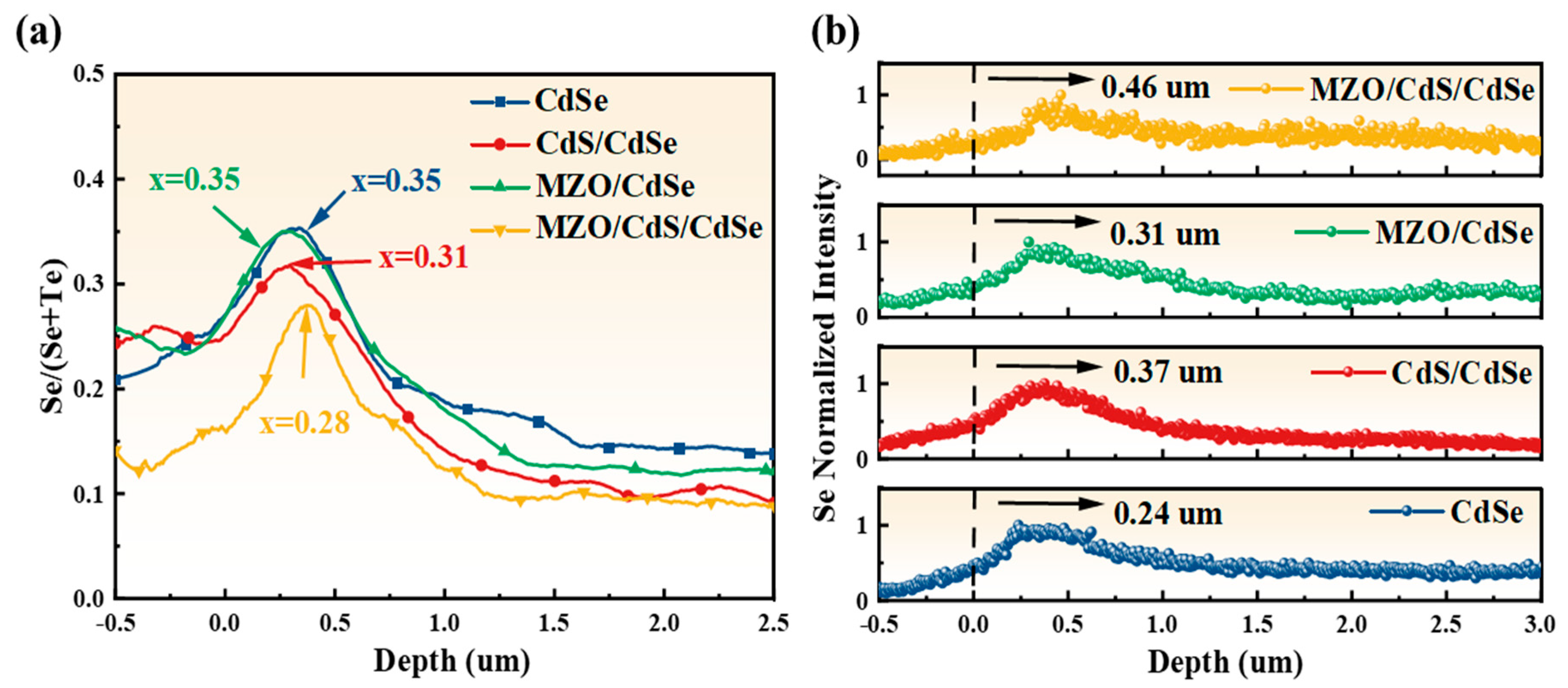
Figure 9: Structures of different window layers (a) Depth profile of Se content in CdSexTe1−x (labeled x denotes the highest Se content in CdSexTe1−x), (b) Normalized Se elemental profiles.
In this paper, we comprehensively analyze four window layer structures for CdSexTe1−x/CdTe solar cells: CdSe, CdS/CdSe, MZO/CdSe, and MZO/CdS/CdSe. We further explore how the choice of window layer affects device performance, carrier recombination mechanisms, pn junction characteristics, and Se distribution.
The results show that the device efficiencies of CdSe and MZO/CdS/CdSe are 15.21% and 14.40%, respectively. These higher efficiency devices also exhibit higher Ea and Rrec, indicating lower non-radiative recombination. The J0 of the two devices are 10−7 mA/cm2, indicating optimal pn junction characteristics. In contrast, devices with CdS/CdSe and MZO/CdSe window layers show relatively lower efficiencies. This is correlated with their lower Ea, lower Rrec, and a higher J0 of 10−6 mA/cm2. These characteristics indicate higher non-radiative recombination. Elemental distribution analysis reveals that although all devices contain the same 120 nm CdSe film, different window layers lead to distinct Se diffusion profiles and different resulting x-values. In S-containing devices, S-Se interdiffusion reduces the x-value of CdSexTe1−x absorbers, thereby limiting the long-wavelength response. Conversely, S-free devices have relatively higher x-values of CdSexTe1−x, enabling long-wavelength response to extend beyond 850 nm. Overall, the CdSe window layer not only offers a simple fabrication process but also ensures both good device efficiency and a favorable Se distribution, making it a highly promising candidate for window layer applications.
Acknowledgement:
Funding Statement: This work was financially supported by the Yibin Municipal Bureau of Science and Technology Unveiled and Hanging Project 2023JB001.
Author Contributions: All authors have made significant contributions to this study. Junyan Tian was responsible for device fabrication, characterization and testing, data processing, and drafting the manuscript. Qingyuan Zhang provided the sample preparation and testing methodology. Lili Wu. proposed the experimental concept and participated in manuscript revision. Guanggen Zeng and Xia Hao contributed to manuscript revision. Wenwu Wang offered the EDS testing platform. Jingquan Zhang provided the instrumentation for device fabrication. All authors reviewed the results and approved the final version of the manuscript.
Availability of Data and Materials: Not applicable.
Ethics Approval: Not applicable. This study did not involve human or animal subjects.
Conflicts of Interest: The authors declare no conflicts of interest to report regarding the present study.
Supplementary Materials: The supplementary material is available online at https://www.techscience.com/doi/10.32604/cl.2026.076362/s1. Figure S1: Temperature-dependent J-V curves for devices with different window layer structures; Figure S2: Normalized Sn distribution profiles with different window layer structures; Table S1: Comparison between J-V measured current density (Jmeasure) and EQE-integrated current density (Jintegrate) for different window layers; Table S2: Summarized VOC-T linear fitting results across the four window layer devices; Table S3: EDS line-scan error statistics for various elements in different window layer devices.
References
1. Sartor BE, Reese SB, Mansfield LM, Muzzio R, Jiang C-S, Colegrove E, et al. Roadmap to 100 GWDC: scientific and supply chain challenges for CdTe photovoltaics. Joule. 2025;102235. doi:10.1016/j.joule.2025.102235. [Google Scholar] [CrossRef]
2. Scarpulla MA, McCandless B, Phillips AB, Yan Y, Heben MJ, Wolden C, et al. CdTe-based thin film photovoltaics: recent advances, current challenges and future prospects. Sol Energy Mater Sol Cells. 2023;255:112289. doi:10.1016/j.solmat.2023.112289. [Google Scholar] [CrossRef]
3. Duenow JN, Dhere RG, Moutinho HR, To B, Pankow JW, Kuciauskas D, et al. CdSxTe1−x Alloying in CdS/CdTe Solar Cells. MRS Proc. 2011;1324:1403. doi:10.1557/opl.2011.1151. [Google Scholar] [CrossRef]
4. Das NK, Farhad SFU, Gupta AKS, Ahamed EMKI, Matin MA, Amin N. The significance of bilayer window (CdS:O/CdS) on the performance of CdTe thin film solar cells. Opt Mater. 2024;155:115816. doi:10.1016/j.optmat.2024.115816. [Google Scholar] [CrossRef]
5. Bosio A, Rosa G, Romeo N. Past, present and future of the thin film CdTe/CdS solar cells. Sol Energy. 2018;175:31–43. doi:10.1016/j.solener.2018.01.018. [Google Scholar] [CrossRef]
6. Kosyachenko LA, Grushko EV, Mathew X. Quantitative assessment of optical losses in thin-film CdS/CdTe solar cells. Sol Energy Mater Sol Cells. 2012;96:231–37. doi:10.1016/j.solmat.2011.09.063. [Google Scholar] [CrossRef]
7. Pandey R, Munshi A, Shimpi T, Shah A, Bothwell A, Kuciauskas D, et al. CdTe-based solar cells with variations in Mg concentration in the MgZnO emitter. Solar RRL. 2021;5(7):2100126. doi:10.1002/solr.202100126. [Google Scholar] [CrossRef]
8. Ren S, Li H, Lei C, Li C, Yin X, Wu L, et al. Interface modification to enhance electron extraction by deposition of a ZnMgO buffer on SnO2-coated FTO in CdTe solar cells. Sol Energy. 2019;177:545–52. doi:10.1016/j.solener.2018.11.053. [Google Scholar] [CrossRef]
9. Li D-B, Song Z, Awni RA, Bista SS, Shrestha N, Grice CR, et al. Eliminating S-Kink To maximize the performance of MgZnO/CdTe solar cells. ACS Appl Energy Mater. 2019;2(4):2896–903. doi:10.1021/acsaem.9b00233. [Google Scholar] [CrossRef]
10. Ren S, Wang H, Li Y, Li H, He R, Wu L, et al. Rapid thermal annealing on ZnMgO window layer for improved performance of CdTe solar cells. Sol Energy Mater Sol Cells. 2018;187:97–103. doi:10.1016/j.solmat.2018.06.033. [Google Scholar] [CrossRef]
11. Wei S-H, Zhang SB, Zunger A. First-principles calculation of band offsets, optical bowings, and defects in CdS, CdSe, CdTe, and their alloys. J Appl Phys. 2000;87(3):1304–11. doi:10.1063/1.372014. [Google Scholar] [CrossRef]
12. Strauss AJ, Steininger J. Phase diagram of the CdTe-CdSe pseudobinary system. J Electrochem Soc. 1970;117(11):1420. doi:10.1149/1.2407335. [Google Scholar] [CrossRef]
13. Tarek El-Shahat M, Ali AS, Hassana AM, Yousef ES, Shaaban ER. Performance-related structural, optical, and electrical characteristics of 2 μm the CdTe-CdSe absorption layer of solar cell. J Ovonic Res. 2023;19(6):705–18. doi:10.15251/JOR.2023.196.705. [Google Scholar] [CrossRef]
14. Rahman MH, Rojsatien S, Krasikov D, Chan MKY, Bertoni M, Mannodi-Kanakkithodi A. First principles investigation of dopants and defect complexes in CdSexTe1−x. Sol Energy Mater Sol Cells. 2025;293:113857. doi:10.1016/j.solmat.2025.113857. [Google Scholar] [CrossRef]
15. Paudel NR, Yan Y. Enhancing the photo-currents of CdTe thin-film solar cells in both short and long wavelength regions. Appl Phys Lett. 2014;105(18):183510. doi:10.1063/1.4901532. [Google Scholar] [CrossRef]
16. Shakil M, Zafar M, Ahmed S, Hashmi MR-u-r, Choudhary MA, Iqbal T. Theoretical calculations of structural, electronic, and elastic properties of CdSe1−xTex: a first principles study. Chin Phys B. 2016;25(7):076104. doi:10.1088/1674-1056/25/7/076104. [Google Scholar] [CrossRef]
17. Wang T, Zhu X, Li W, Zhang J, Wang W. Incorporation of metal selenide thin films as the secondary absorber in the CdTe solar cells. J Alloys Compd. 2020;828:154415. doi:10.1016/j.jallcom.2020.154415. [Google Scholar] [CrossRef]
18. Swanson DE, Sites JR, Sampath WS. Co-sublimation of CdSexTe1−x layers for CdTe solar cells. Sol Energy Mater Sol Cells. 2017;159:389–94. doi:10.1016/j.solmat.2016.09.025. [Google Scholar] [CrossRef]
19. Frouin B, Bidaud T, Pirotta S, Ablekim T, Moseley J, Metzger WK, et al. Quantitative assessment of selenium diffusion and passivation in CdSeTe solar cells probed by spatially resolved cathodoluminescence. APL Mater. 2024;12(3):0195398. doi:10.1063/5.0195398. [Google Scholar] [CrossRef]
20. Fiducia TAM, Mendis BG, Li K, Grovenor CRM, Munshi AH, Barth K, et al. Understanding the role of selenium in defect passivation for highly efficient selenium-alloyed cadmium telluride solar cells. Nat Energy. 2019;4(6):504–11. doi:10.1038/s41560-019-0389-z. [Google Scholar] [CrossRef]
21. Poplawsky JD, Guo W, Paudel N, Ng A, More K, Leonard D, et al. Structural and compositional dependence of the CdTexSe1−x alloy layer photoactivity in CdTe-based solar cells. Nat Commun. 2016;7(1):12537. doi:10.1038/ncomms12537. [Google Scholar] [CrossRef]
22. Bowman AR, Leaver JF, Frohna K, Stranks SD, Tagliabue G, Major JD. Spatially resolved photoluminescence analysis of the role of Se in CdSexTe1−x thin films. Nat Commun. 2024;15(1):8729. doi:10.1038/s41467-024-52889-z. [Google Scholar] [CrossRef]
23. Zheng X, Kuciauskas D, Moseley J, Colegrove E, Albin DS, Moutinho H, et al. Recombination and bandgap engineering in CdSeTe/CdTe solar cells. APL Mater. 2019;7(7):5098459. doi:10.1063/1.5098459. [Google Scholar] [CrossRef]
24. Zheng X, Colegrove E, Duenow JN, Moseley J, Metzger WK. Roles of bandgrading, lifetime, band alignment, and carrier concentration in high-efficiency CdSeTe solar cells. J Appl Phys. 2020;128(5):0013726. doi:10.1063/5.0013726. [Google Scholar] [CrossRef]
25. Jiang H, Cai Y, Wang G, Yi K, Liu F, Tian J, et al. Buried junction and efficient carrier separation in CdSexTe1−x/CdTe solar cells. J Appl Phys. 2024;135(14):0188812. doi:10.1063/5.0188812. [Google Scholar] [CrossRef]
26. Halim MA, Islam MM, Luo X, Sakurai T, Sakai N, Kato T, et al. A comparative study on charge carrier recombination across the junction region of Cu2ZnSn(S,Se)4 and Cu(In,Ga)Se2 thin film solar cells. AIP Adv. 2016;6(3):4944911. doi:10.1063/1.4944911. [Google Scholar] [CrossRef]
27. Fang X, Ren S, Li C, Li C, Chen G, Lai H, et al. Investigation of recombination mechanisms of CdTe solar cells with different buffer layers. Sol Energy Mater Sol Cells. 2018;188:93–8. doi:10.1016/j.solmat.2018.08.015. [Google Scholar] [CrossRef]
28. Scheer R. Activation energy of heterojunction diode currents in the limit of interface recombination. J Appl Phys. 2009;105(10):3126523. doi:10.1063/1.3126523. [Google Scholar] [CrossRef]
29. Yuan Y, Yan G, Hong R, Liang Z, Kirchartz T. Quantifying efficiency limitations in all-inorganic halide perovskite solar cells. Adv Mater. 2022;34(21):202108132. doi:10.1002/adma.202108132. [Google Scholar] [CrossRef]
30. Carron R, Andres C, Avancini E, Feurer T, Nishiwaki S, Pisoni S, et al. Bandgap of thin film solar cell absorbers: a comparison of various determination methods. Thin Solid Films. 2019;669:482–86. doi:10.1016/j.tsf.2018.11.017. [Google Scholar] [CrossRef]
31. Govindharajulu Srinivasan M, Anandan R, Madaka R, Rath Jatindra K, Piraviperumal M. Influence of Substrate on Sb2Se3/CdS Heterojunction Thin Film Solar Cells and Evaluation of Their Performance by Dark J-V Analysis. Prog Photovolt Res Appl. 2024;33(2):357–71. doi:10.1002/pip.3853. [Google Scholar] [CrossRef]
32. Obradović A, Toch K, Coppens B, Khelifi S, Lauwaert J, Thybaut J. Non-isothermal modeling of dark current-voltage measurements of a CIGS solar cell. ECS J Solid State Sci Technol. 2018;7(2):P50–4. doi:10.1149/2.0101802jss. [Google Scholar] [CrossRef]
33. Guerrero A, Bisquert J, Garcia-Belmonte G. Impedance spectroscopy of metal halide perovskite solar cells from the perspective of equivalent circuits. Chem Rev. 2021;121(23):14430–84. doi:10.1021/acs.chemrev.1c00214. [Google Scholar] [CrossRef]
34. Prayogi S, Ristiani D, Darminto D. Unravelling the electrochemical impedance spectroscopy of hydrogenated amorphous silicon cells for photovoltaics. Mater Renew Sustain Energy. 2025;14(1):17. doi:10.1007/s40243-024-00295-2. [Google Scholar] [CrossRef]
35. Jun H, Tondelier D, Geffroy B, Florea I, Bouree J-E, Lopez-Varo P, et al. Electrochemical and spectro-microscopic analyses of charge accumulation and ion migration in dry processed perovskite solar cells under electrical biasing. J Phys Chem Lett. 2025;16(3):835–47. doi:10.1021/acs.jpclett.4c02884. [Google Scholar] [CrossRef]
36. Hongsith K, Yarangsi V, Sucharitakul S, Phadungdhitidhada S, Ngamjarurojana A, Choopun S. A multi-electron transporting layer for efficient perovskite solar cells. Coatings. 2021;11(9):1020. doi:10.3390/coatings11091020. [Google Scholar] [CrossRef]
37. Patil SS, Bhosale PN. Optimization and comparative evaluation of optoelectronic properties of hydrothermally synthesized CdIn2Te4thin films: PEC performance. Mater Res Express. 2019;6(12):126404. doi:10.1088/2053-1591/ab5500. [Google Scholar] [CrossRef]
38. Avancini E, Keller D, Carron R, Arroyo-Rojas Dasilva Y, Erni R, Priebe A, et al. Voids and compositional inhomogeneities in Cu(In,Ga)Se2 thin films: evolution during growth and impact on solar cell performance. Sci Technol Adv Mater. 2018;19(1):871–82. doi:10.1080/14686996.2018.1536679. [Google Scholar] [CrossRef]
39. Gershon T, Sardashti K, Gunawan O, Mankad R, Singh S, Lee YS, et al. Photovoltaic device with over 5% efficiency based on an n-type Ag2ZnSnSe4 absorber. Adv Energy Mater. 2016;6(22):1601182. doi:10.1002/aenm.201601182. [Google Scholar] [CrossRef]
40. Major JD, Bowen L, Treharne R, Durose K. Assessment of photovoltaic junction position using combined focused ion beam and electron beam-induced current analysis of close space sublimation deposited CdTe solar cells. Prog Photovolt Res Appl. 2014;22(10):1096–104. doi:10.1002/pip.2507. [Google Scholar] [CrossRef]
41. Seitz F. On the porosity observed in the Kirkendall effect. Acta Metall. 1953;1(3):355–69. doi:10.1016/0001-6160(53)90112-6. [Google Scholar] [CrossRef]
42. Neupane S, Li D-B, Jamarkattel MK, Abudulimu A, Jiang C-S, Bista SS, et al. Evaporated CdSe for efficient polycrystalline CdSeTe thin-film solar cells. ACS Energy Lett. 2024;9(12):6233–37. doi:10.1021/acsenergylett.4c02874. [Google Scholar] [CrossRef]
43. Hatton P, Abbas A, Kaminski P, Yilmaz S, Watts M, Walls M, et al. Inert gas bubble formation in magnetron sputtered thin-film CdTe solar cells. Proc R Soc A. 2020;476(2239):20200056. doi:10.1098/rspa.2020.0056. [Google Scholar] [CrossRef]
44. Greenhalgh R, Hatton P, Kornienko V, Abbas A, Goddard P, Smith R, et al. The origins of void formation in sputtered CdSe. In: Proceedings of the 2021 IEEE 48th Photovoltaic Specialists Conference (PVSC); 2021 Jun 20–25; Fort Lauderdale, FL, USA. doi:10.1109/PVSC43889.2021.9519113. [Google Scholar] [CrossRef]
45. Sanchez AM, Dimitrakopulos GP, Ruterana P. Mechanism for pinhole formation in GaN/AlN/Si(111) layers from steps at the substrate surface. Appl Phys Lett. 2005;86(1):1845599. doi:10.1063/1.1845599. [Google Scholar] [CrossRef]
46. Lin C, Naramoto H, Xu Y, Kitazawa S-i, Narumi K, Sakai S. Formation of nano-sized pinholes array in thin Ni film on MgO(100) substrate. Thin Solid Films. 2003;443(1–2):28–32. doi:10.1016/S0040-6090(03)00527-3. [Google Scholar] [CrossRef]
47. Baines T, Zoppi G, Bowen L, Shalvey TP, Mariotti S, Durose K, et al. Incorporation of CdSe layers into CdTe thin film solar cells. Sol Energy Mater Sol Cells. 2018;180:196–204. doi:10.1016/j.solmat.2018.03.010. [Google Scholar] [CrossRef]
48. Baines T, Bowen L, Mendis BG, Major JD. Microscopic analysis of interdiffusion and void formation in CdTe1–xSex and CdTe layers. ACS Appl Mater Interfaces. 2020;12(34):38070–5. doi:10.1021/acsami.0c09381. [Google Scholar] [CrossRef]
49. Jamarkattel MK, Phillips AB, Li D-B, Bastola E, Liyanage GK, Friedl JD, et al. High vacuum heat-treated MZO: Increased n-type conductivity and elimination of S-kink in MZO/CdSe/CdTe solar cells. MRS Adv. 2022;7(30):713–7. doi:10.1557/s43580-022-00341-z. [Google Scholar] [CrossRef]
50. Wu Q, Li R, Zhang Y, Huang K, Li H, Liu X. Optimizing the band alignment of the MZO/CdSeTe/CdTe solar cell by varying the substrate temperature of MZO film. Energies. 2024;17(3):592. doi:10.3390/en17030592. [Google Scholar] [CrossRef]
51. Ablekim T, Duenow JN, Zheng X, Moutinho H, Moseley J, Perkins CL, et al. Thin-film solar cells with 19% efficiency by thermal evaporation of CdSe and CdTe. ACS Energy Lett. 2020;5(3):892–6. doi:10.1021/acsenergylett.9b02836. [Google Scholar] [CrossRef]
52. Qin J-M, Cao J-M, Jiang D-Y. Growth and characterization of the Mg0.57Zn0.43O alloy film. Acta Physica Sinica. 2013;62(13):138101. doi:10.7498/aps.62.138101. [Google Scholar] [CrossRef]
53. Thapa D, Huso J, Lapp J, Rajabi N, Morrison JL, McCluskey MD, et al. Thermal stability of ultra-wide-bandgap MgZnO alloys with wurtzite structure. J Mater Sci Mater Electron. 2018;29(19):16782–90. doi:10.1007/s10854-018-9772-y. [Google Scholar] [CrossRef]
54. Das AK, Misra P, Ajimsha RS, Bose A, Joshi SC, Porwal S, et al. Effect of Mg diffusion on photoluminescence spectra of MgZnO/ZnO bi-layers annealed at different temperatures. J Appl Phys. 2013;114(18):4830010. doi:10.1063/1.4830010. [Google Scholar] [CrossRef]
55. Li C, Wang A, Wu L, He X, Zhang J, Hao X, et al. Investigations of the structural, optical properties and electronic structure of CdTe1−xSex films fabricated by RF magnetron sputtering. Mater Res Express. 2019;6(6):066415. doi:10.1088/2053-1591/ab109c. [Google Scholar] [CrossRef]
56. Reyes-Banda MG, Regalado-Perez E, Pintor-Monroy MI, Hernández-Gutiérrez CA, Quevedo-López MA, Mathew X. Effect of Se diffusion and the role of a thin CdS buffer layer in the performance of a CdSe/CdTe solar cell. Superlattices Microstruct. 2019;133:106219. doi:10.1016/j.spmi.2019.106219. [Google Scholar] [CrossRef]
Cite This Article
 Copyright © 2026 The Author(s). Published by Tech Science Press.
This work is licensed under a Creative Commons Attribution 4.0 International License , which permits unrestricted use, distribution, and reproduction in any medium, provided the original work is properly cited.
 Downloads
 Citation Tools