
 Open Access
ISSN:1584-8663 (online)
Publication Frequency:Monthly


Chalcogenide Letters is published monthly (12 issues per year), covering a wide range of fundamental and applied research in the field of chalcogenide materials. The journal is open to letters, short communications and breakings news inserted as Short Notes, in the field of chalcogenide materials either amorphous or crystalline. Short papers in structure, properties and applications, as well as those covering special properties in nano-structured chalcogenides are admitted. Papers based on chalcogenide advanced nanomaterials with possible applications in electronics, optoelectronics, and photonics are encouraged. Also, articles on alternative and renewable energy sources in the field of chalcogenides are accepted for submission. Cross-fertilization of both crystalline and amorphous field in this special class of materials is one of the purposes of this Journal.
Science Citation Index Expanded (SCIE): 2025 Impact Factor 1.6; Web of Science; Scopus Citescore (Impact per Publication 2024): 2.2; SNIP (Source Normalized Impact per Paper 2024): 0.637; Journal Citation Reports (JCR); Google Scholar; CROSSREF; ROAD; OPENALEX.
Effective starting from the first issue of 2026, the Chalcogenide Letters (CL) will be published by Tech Science Press (TSP). This transition is designed to enhance the journal’s academic impact and global visibility while ensuring an improved publishing experience for researchers. The journal's aims, scope, and formatting guidelines will remain unchanged. The journal's Editor-in-Chief, Prof. Ching-Hwa Ho, and the editorial board will continue to lead the iournal toward an even more successful future.
We appreciate the ongoing support of our authors, reviewers, and readers as we embark on this exciting new chapter.
 Open Access
ARTICLE
Chalcogenide Letters, Vol.23, No.6, 2026, DOI:10.32604/cl.2026.083101 - 02 July 2026
(This article belongs to the Special Issue: Chalcogenide Thin Films and Solar Cells for Optoelectronic Applications)
Abstract This study presents a comparative investigation of the structural, DC electrical, and magnetic properties of pure cadmium sulfide (CdS) and 10% chromium-doped CdS (Cd0.9Cr0.1S) nanocrystalline thin films deposited by thermal evaporation. X-ray diffraction analysis confirmed the polycrystalline hexagonal (wurtzite) structure of both films with no detectable secondary phases. Upon Cr doping, the full width at half maximum (FWHM) of the principal diffraction peaks increased systematically, leading to a reduction in average crystallite size from 19.8 nm to 13.9 nm, accompanied by an increase in lattice strain (from 2.48 to 3.52) × 10−3 and dislocation density (from… More >
Open Access
ARTICLE
Chalcogenide Letters, Vol.23, No.6, 2026, DOI:10.32604/cl.2026.079657 - 02 July 2026
Abstract Thin films of CuxZn1−xS nanocomposite with varying copper content (x = 0.3, 0.5, and 0.7) were successfully synthesized by the pulsed laser deposition (PLD) technique from their fabricated powders by the precipitation method for optoelectronic applications. The impact of Cu content on the film’s structural, morphological, optical, and electrical characteristics was investigated. Elemental composition analyses indicated that thin CZS films consisted only of their constituent elements and were free of any noted impurities. XRD patterns demonstrated that all as-grown thin films were polycrystalline in nature and adopted various planes and phases of CuS and ZnS binary… More >
Open Access
ARTICLE
Chalcogenide Letters, Vol.23, No.6, 2026, DOI:10.32604/cl.2026.083065 - 02 July 2026
Abstract The human exposure to hazardous ionizing radiation is increased due to the progression of nuclear technology across energy, medicine, and industrial sectors, etc. Developing transparent shielding materials is essential to overcome the structural and opacity limitations of traditional materials like concrete. The 30TeO2-xPbO2-xBi2O3-(70 − 2x)B2O3 (x = 10, 12, 14 and 16 mol%) glasses are prepared via the melt-quenching technique. The density (ρ) increases from 4.759 to 5.561 g cm−3 due to the incorporation of heavy metal oxides (HMOs). The molar volume (Vm) increases from 32.194 to 33.657 cm3 mol−1. The oxygen packing density (OPD) decreased from 80.761… More >
Open Access
ARTICLE
Chalcogenide Letters, Vol.23, No.6, 2026, DOI:10.32604/cl.2026.077357 - 02 July 2026
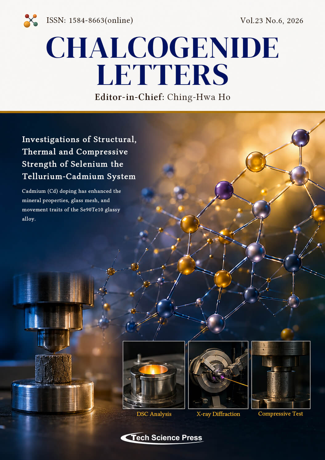
Abstract Cadmium (Cd) doping has enhanced the mineral properties, glass mesh, and movement traits of the Se90Te10 glassy alloy. The (Se90Te10)95Cd5 alloy has a strength 0.032 kN, accompanied by limited ductility, and displays brittle fracture behavior typical of amorphous chalcogenide glasses. (DSC) at varying heating rates was employed to examine the crystallization kinetics in bulk Se90Te10 and (Se90Te10)95Cd5 compositions; X-ray diffraction analysis was utilized to identify the crystalline structure of Se90Te10 and (Se90Te10)95Cd5, confirming the non-crystalline nature of both materials. Various kinetic frameworks were developed utilizing activation energies for glass transition and crystallization processes. “The Kissinger equation” was employed More >
Open Access
ARTICLE
Chalcogenide Letters, Vol.23, No.6, 2026, DOI:10.32604/cl.2026.082939 - 02 July 2026
Abstract Using first principles calculations, we have systematically studied the structural, elastic, mechanical, lattice dynamic, and thermodynamic properties of the CuBS2 semiconductor. The calculated structural parameters are in good agreement with the experimental values. The obtained elastic constants confirm that the compound is mechanically stable. The B/G ratio of CuBS2 indicating that this crystal possesses ductile characteristics. Using the ELATE software, 3D and 2D visualizations of anisotropic elastic properties, namely, the maximum and minimum values of Young’s modulus (E), shear modulus (G), linear compressibility (β), and Poisson’s ratio (ν), have been analyzed. Furthermore, we calculated the elastic anisotropy index (AU, AB,… More >
Open Access
ARTICLE
Chalcogenide Letters, Vol.23, No.6, 2026, DOI:10.32604/cl.2026.085590 - 02 July 2026
Abstract The major challenge in developing efficient photovoltaic devices is achieving highlight absorption, optimal charge transport, and low recombination losses. In this work, the effect of the immersion bath numbers in the chemical bath deposition (CBD) technique on the properties of bismuth oxysulfide (Bi2O2S) thin films, as emergent materials, was studied. The films were synthesized under eco-friendly conditions, using a low-concentration bismuth nitrate precursor and thioacetamide as the sulfur source, and under basic conditions at moderate temperature, with a reaction time of 3 h. X-ray diffraction demonstrated the formation of a crystalline Bi2O2S phase, and the morphological… More >

 Submit a Paper
 Propose a Special lssue