
 Submit a Paper
 Propose a Special lssue
 Open Access
ARTICLE

Engineering and Tuning of Absorber Layer Properties for High-Efficiency SnS-Based Solar Cells: A SCAPS-1D Simulation Study
1 Laboratory of Optoelectronics and Components, Department of Physics, Faculty of Science, Setif-1 University, Setif, 19000, Algeria
2 Laboratory of Photonics Systems and Nonlinear Optics, Institute of Optics and Precision Mechanics, Setif-1 University, Setif, 19000, Algeria
* Corresponding Author: Abdelhak Nouri. Email:
Chalcogenide Letters 2026, 23(1), 6 https://doi.org/10.32604/cl.2026.076586
Received 23 September 2025; Accepted 23 November 2025; Issue published 26 January 2026
 View Full Text
 Download PDF
Abstract
This work uses numerical modeling in SCAPS-1D to examine the efficiency analysis of a solar cell based on SnS. The power conversion efficiency (PCE) is limited to 24.5% because of incomplete photon absorption in the absorber layer (SnS) and carrier recombination. To increase the absorption window, facilitate charge mobility, and suppress bulk recombination at the rear contact, the absorbent film was divided up into three sublayers with graded band gaps of 1.1 eV, 1.2 eV, and 1.3 eV. Furthermore, the sublayers’ linear gradient doping improved charge collection while simultaneously lowering recombination at the interface. A compromise between photon absorption and carrier extraction is made possible by this physical and geometrical optimization of the standard cell. It also reveals that the optimal sublayer thicknesses are 500 nm for SnS-1, 500 nm for SnS-2, and 1600 nm for SnS-3, which allows a sharp improvement in PCE of 28.45%. Furthermore, further optimization by adjusting the thickness of the absorbent underlays achieves an efficiency of 31.5% with a significant fill factor (FF) of 86.6%. These results confirm that the physical and geometrical optimization (thickness, band gap, charge distribution) of solar cell based SnS thin films has an important contribution in the improvement of the efficiency of cells.Keywords
Solar cells based on thin film have effectively meet the growing electricity needs, and with technological advancements, the demand for these cells has increased significantly in recent decades. In fact, CuInGaSe2 (CIGS) and CdTe, CuInS2 (CIS) cells have attracted high interest from thin-film technology researchers in the photovoltaic sector. In addition, the toxic risks associated with cadmium (Cd), the nonabundance in nature, and the high cost of indium (In), gallium (Ga), and tellurium (Te) constitute practical obstacles to the manufacture and commercialization of these types of cells. Thus, this circumstance leads to a pressing need to find the materials of less hazardous and more prevalent elements [1].
The solar cells based on tin sulfide (SnS) as absorber material provide a viable economic alternative. SnS is a semiconductor that has elements of inexpensiveness and environmental friendliness. Its direct band gap of 1.3 eV and an absorption coefficient of over 104 cm−1 make it physically appealing [2]. In addition, typically, ZnO/CdS/SnS is the conventional heterojunction for these cells, where ZnO is the window layer, CdS is the buffer layer, and SnS is the primary absorber layer. Moreover, even with continuous advancements, the experimental efficacy conversion of SnS based solar cells remains lower than that of other technologies. Therefore, research is still being done to find further optimization of these structures [3].
The conventional ZnO/CdS/SnS heterostructure has been investigated using both experimental and theoretical analysis. Subsequently, studies have shown that the conversion efficiency (PCE) of SnS-based cells has remained low, often less than 8%, despite continuous improvements in manufacturing procedures [4]. On the other hand, SCAPS-1D numerical simulations suggest that efficiency of up to 26.9% might be possible with buffer and back surface field layers tuned [5]. This reveals the significant gap between theoretical predictions and experimental results, which can be closed to fully utilize ZnO/CdS/SnS solar cells through appropriate interface engineering, defect passivation, and optimal layer design.
In this context, considerable research is being done in this area to enhance this kind of cell and boost its effectiveness. Numerical simulation techniques help these efforts by offering a systematic method to investigate the effects of essential parameters such as doping density and layer thickness on the design of highly efficient structures [6]. The most widely used and powerful of these tools is SCAPS-1D, a simulation program that is particularly well-suited for examining thin-film solar cells and offering comprehensive insights into their electrical and optical performance under varied design circumstances [7].
The ZnO/CdS/SnS heterojunction solar cell was modeled and examined in this work, and SCAPS-1D was used to assess its viability and preliminary performance. The goal is to optimize the power conversion efficiency by varying the thickness and doping density of the SnS absorber layer.
Although numerous software tools are available for solar photovoltaic modeling. Among them SCAPS-1D was chosen for with a focus on thin-film photovoltaic simulations that can support up to seven structural levels. It is primarily designed to simulate and calculate principles photovoltaic parameters.
With the right boundary conditions, SCAPS-1D can solve basic semiconductor equations such as Poisson’s equation and current equations [8].
Poisson’s equation
Electron and hole charge conservation, including generation and recombination, is expressed by the continuity equations:
For electrons:
For holes:
Drift and diffusion components are included in the current densities:
Fig. 1 illustrates the typical solar cell studied, where ZnO, CdS, and SnS serve as window, buffer, and absorber layers, respectively. Furthermore, Table 1 collects the parameters of the layers that make up the cell extracted from the work of Boubakri et al. [9]. The sequence of this simulation work was carried out as follows:
- 1.The first step is to calculate the main characteristics of the typical cell (Vco, Jsc, FF, PCE) versus doping concentration and the thickness of the absorber layer (SnS).
- 2.The second step is to define appropriate buffer thickness (CdS) by fixing the thickness of SnS (varying the thickness of the CdS).
- 3.Thirdly, the previous steps aim to determine the efficiency achievable by the cell with the best fill factor (FF) value. Subsequently, we propose optimizing the cell architecture to enhance efficiency.
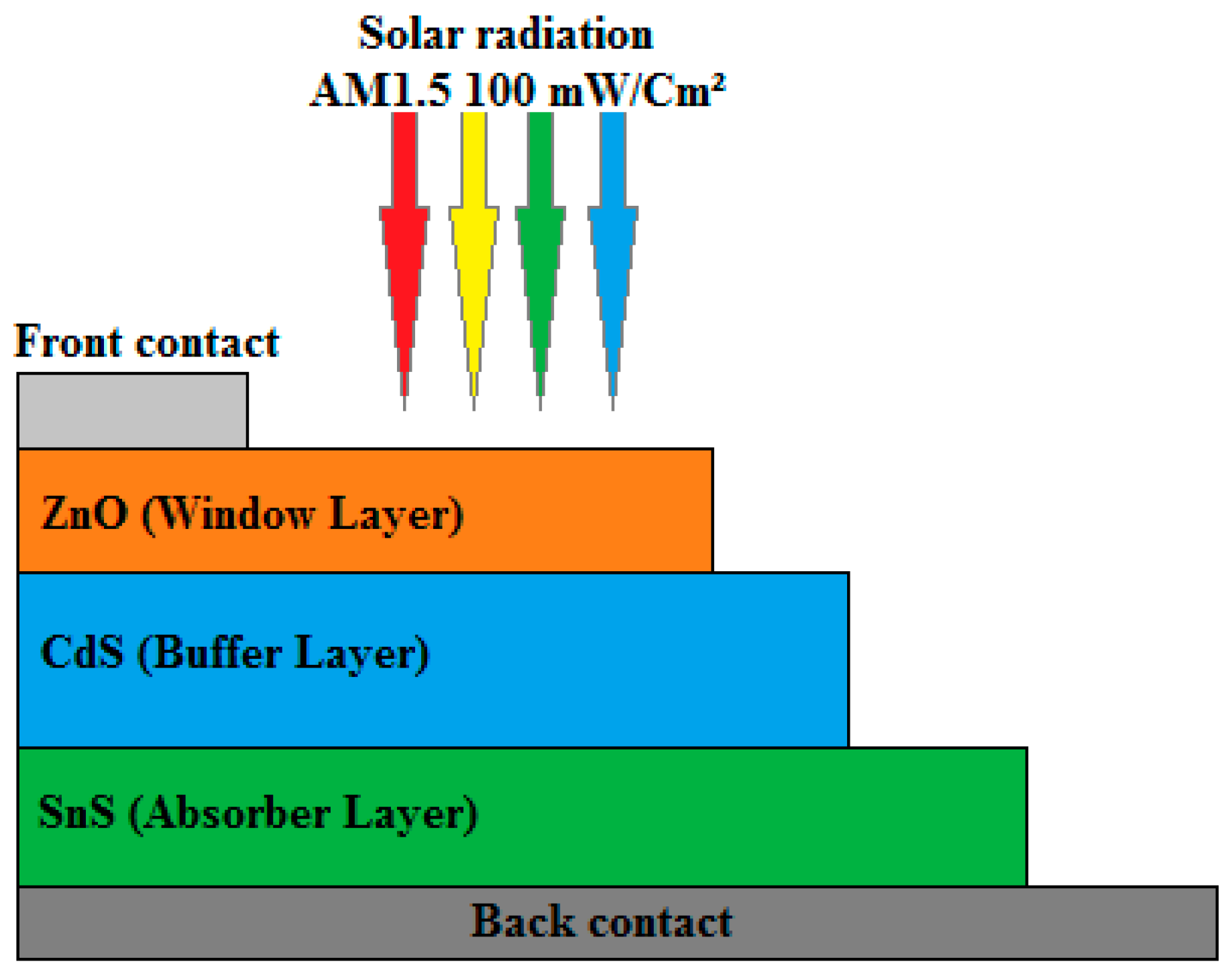
Figure 1: Schematic diagram view of a typical SnS-based solar cell.
Table 1: Parameters set for the simulation of a typical SnS-based solar cell.
| Parameters | ZnO | CdS | SnS |
|---|---|---|---|
| Eg (eV) | 3.35 | 2.42 | 1.3 |
| Χ (eV) | 4.5 | 4.4 | 4.1 |
| εr | 9 | 10 | 13 |
| Nc (cm−3) | 2.2 × 10¹⁸ | 2.2 × 10¹⁸ | 1.8 × 10¹⁸ |
| Nv (cm−3) | 1.8 × 10¹⁹ | 1.7 × 10¹⁹ | 4.76 × 10¹⁸ |
| μn (cm2/V·s) | 100 | 340 | 15 |
| μp (cm2/V·s) | 25 | 50 | 100 |
| NA, ND (cm−3) | 1018 | 1018 | 1015–1016 |
The simulation parameters were set to 300 K, infinite shunt resistance, series resistance null, and the sun spectrum AM1.5. The incident power density was set at 100 mW/cm2, equivalent to one-sun illumination. So, at this step, So, at this step, CdS buffer layer thickness was held constant so that an explicit analysis could be made regarding the influence of variations in SnS on total photovoltaic performance in ZnO/CdS/SnS cells.
3.1 Effect of Absorber Layer Thickness
Fig. 2 shows the Voc and Jsc plotted vs. SnS thickness. Voc increases significantly and almost linearly with increasing SnS thickness, 0.70 V at 100 nm to 0.95 V at 3000 nm, indicating that the thicker absorber layer favors more charge carrier generation and separation with probably reduced recombination at the junction interfaces. The increasing Voc voltage is described as the improvement of the quality of the layer and the junction with thickness due to reduced surface defects plus better crystal maturity attained in thicker layers since carrier diffusion will be enhanced and recombination losses minimized.
As shown in Fig. 2, the Jsc current density Jsc keeps a great increasing trend from 18 mA/cm2 at 100 nm up to 36 mA/cm2 at 3000 nm. Such a substantial, almost doubling increase is directly related to better photon absorption; increasing SnS layer thickness means more photons are acquired, hence more electron-hole pairs are built; therefore, photogenerated current increases. The Jsc curve shows gradual saturation beyond 1000 nm (Fig. 2), which means absorption has reached maximum, and further thickness brings very marginal gains, probably due to the limited diffusion length of carriers or intrinsic absorption coefficients of the material as reported by Dekhil et al. [10] and Reddy et al. [11].
Furthermore, Fig. 3 depicts the variation of fill factor (FF) and the efficiency (PCE) versus the thickness of absorber layer SnS. The nonlinear nonmonotonic evolution of the (FF) fills in compensation phenomena. It falls from 81% at 100 nm to 75.6% at 500 nm, followed by an exponential increase attaining a maximum value of 77.6% around 1500 nm and then falling again to stabilize at 75% at 3000 nm. A sharp drop at the beginning can be due to increasing series resistance as well as recombination in the ultrathin layer region where inhomogeneity and interfacial defects dominate. The rise up to 1500 nm is a manifestation of better crystal quality and carrier collection that have been obtained due to optimized thicknesses, resistances, and recombination being minimized. The decrease in FF manifests itself as charge transport limitations when the thickness exceeds 1500 nm. This thickness causes the appearance of additional series resistance and significant volume recombination, which impedes charge mobility and consequently collection efficiency.
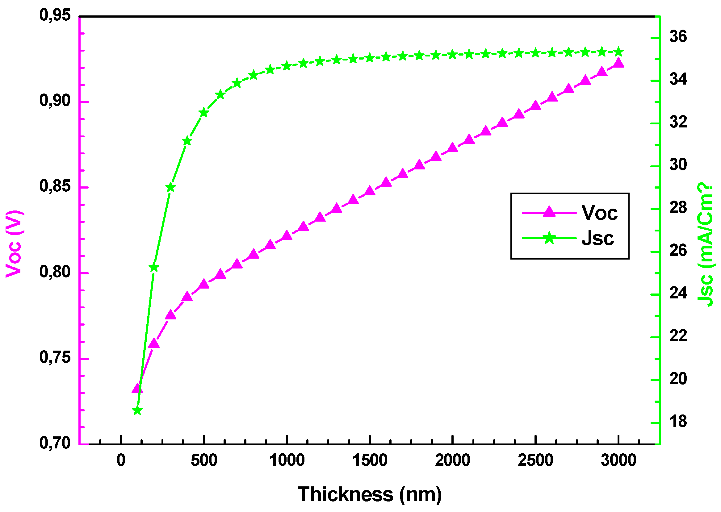
Figure 2: Effect of the absorber layer (SnS) thickness on the open-circuit voltage Voc and the short-circuit current Jsc.
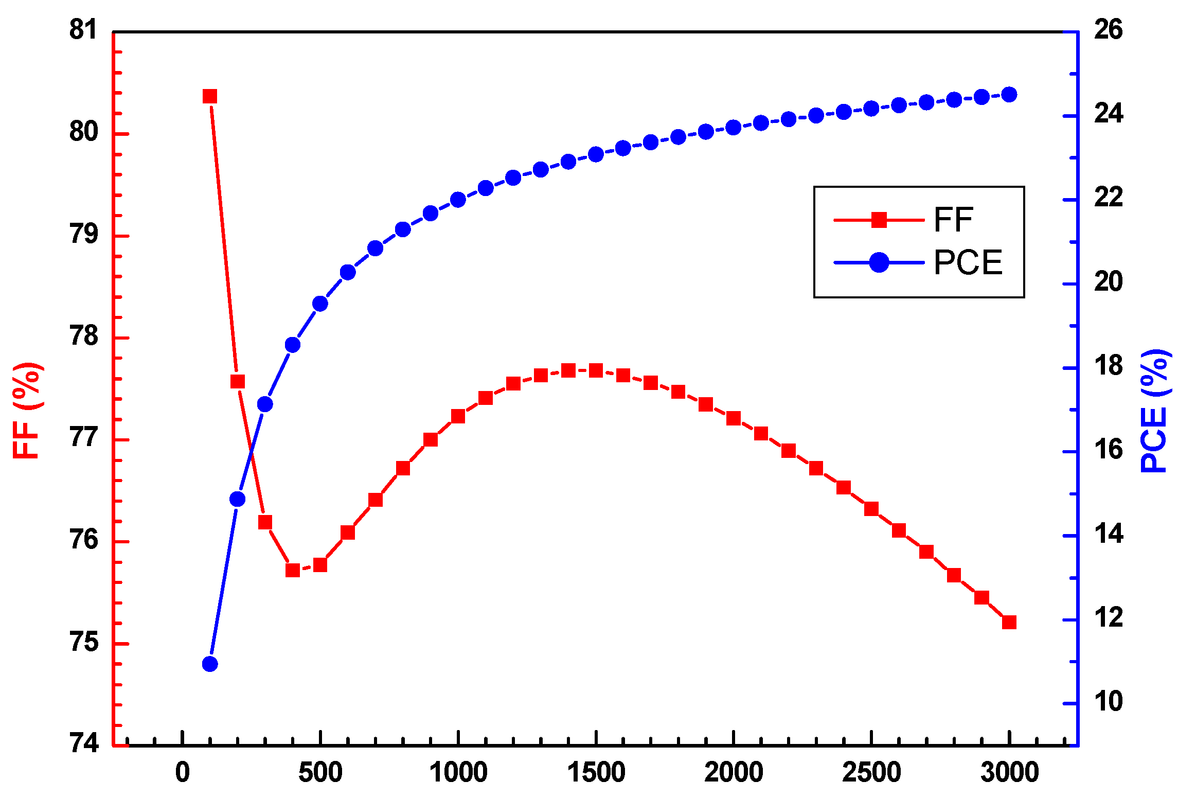
Figure 3: Influence of the thickness of the absorber layer (SnS) on power efficiency conversion (PCE) and fill factor (FF).
However, when these three factors are combined, the efficiency (PCE) shows a remarkable exponential rise, rising from 10% at 100 nm to 26% at 3000 nm. The notable improvement highlights the immense effect of large increases in Vco and Jsc, even if there was only a slight variation in FF. The product Vco × Jsc × FF indicates that at large thicknesses, increases in voltage and current would more than make up for even little fill factor decrease. The performance would be harmonized and optimized at this optimum thickness, which was found at about 1500 nm. This is an ideal compromise point where the fill factor reaches its maximum value and Voc and Jsc are already high. Voc and Jsc are over 0.85 V and 30 mA/cm2, respectively, with an optimized fill factor of roughly 77.6% to maximize overall efficiency. This thickness is close to the optimal PCE.
3.2 Effect of Doping Concentration
In this section, the effect of carrier concentration (doping) is investigated by fixing the SnS absorber thickness at 1500 nm and the CdS buffer layer at 500 nm. This analysis highlights how varying doping levels influence overall device performance, including efficiency; fill factor (FF), Voc voltage, and Jsc current density.
The influence of doping density on Voc voltage, and Jsc current density of the SnS layer are depicted in Fig. 4. The built-in electric field increases with higher carrier density in such a way that the Voc voltage increases. Thus, Voc has a logarithmic dependence on carrier concentration as per the diode equation and therefore increases with an increase in carrier concentration. Increased SnS conductivity will increase Jsc due to better charge collection, and thus there exists an optimum value for which Jsc is maximum, as shown in Fig. 4. Voc increases with increased doping up to the point where other recombination mechanisms set in, especially Auger recombination at very high doping levels, and carriers cannot be separated well enough due to limited depth of absorption resulting from high free-carrier absorption [12].
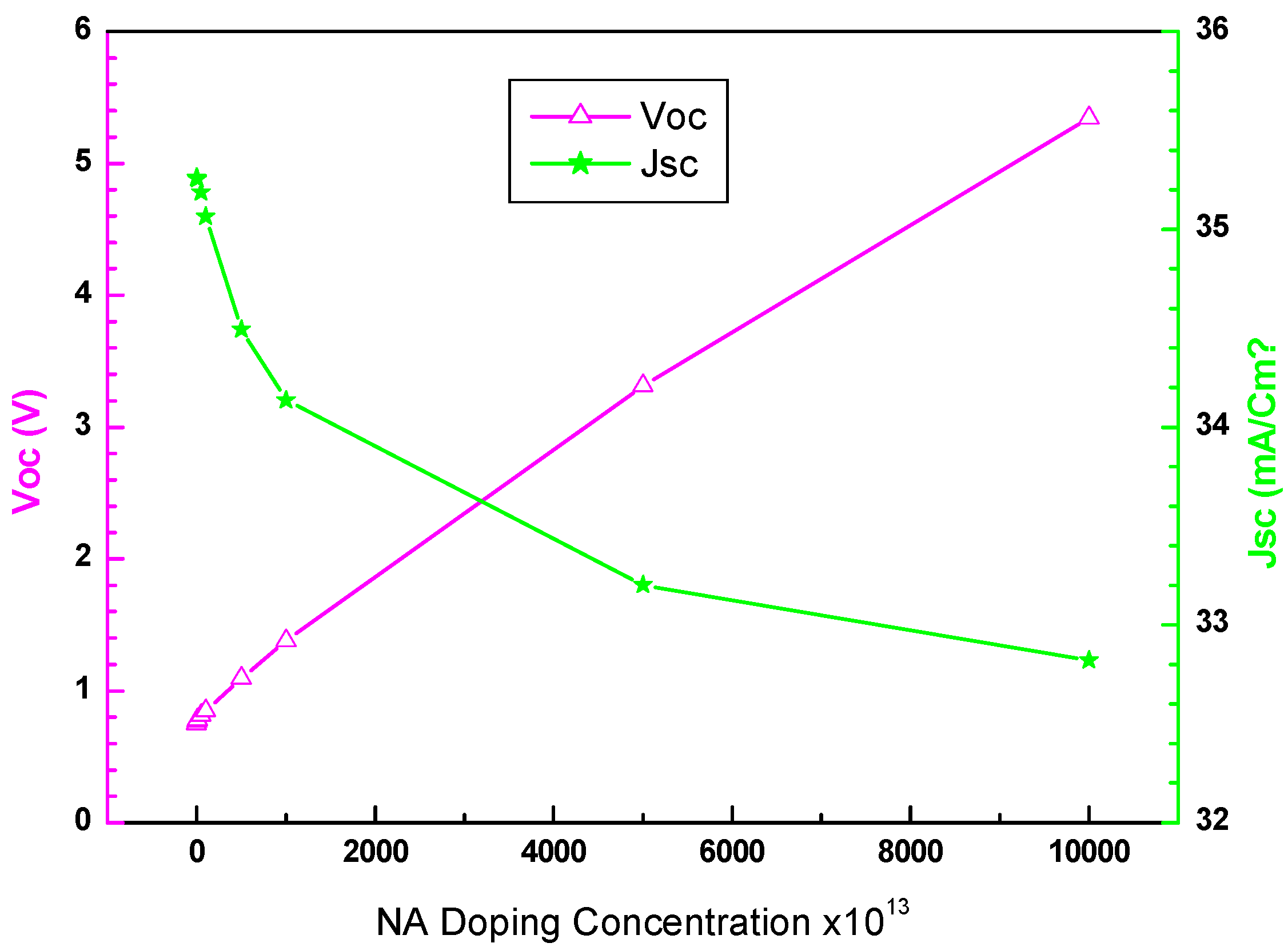
Figure 4: The effect of NA doping concentration of absorber layer (SnS) on Voc and Jsc.
Furthermore, the trade-off between the FF and PCE versus the carrier concentration are illustrated in Fig. 5. The FF evidently begins to degrade in the region between 1014 and 1017 cm−3 carrier concentration in SnS where it can be maintained at a relatively high value, near 82% for low doping, gradually falling off to near 72% at the highest concentration as shown in Fig. 5.
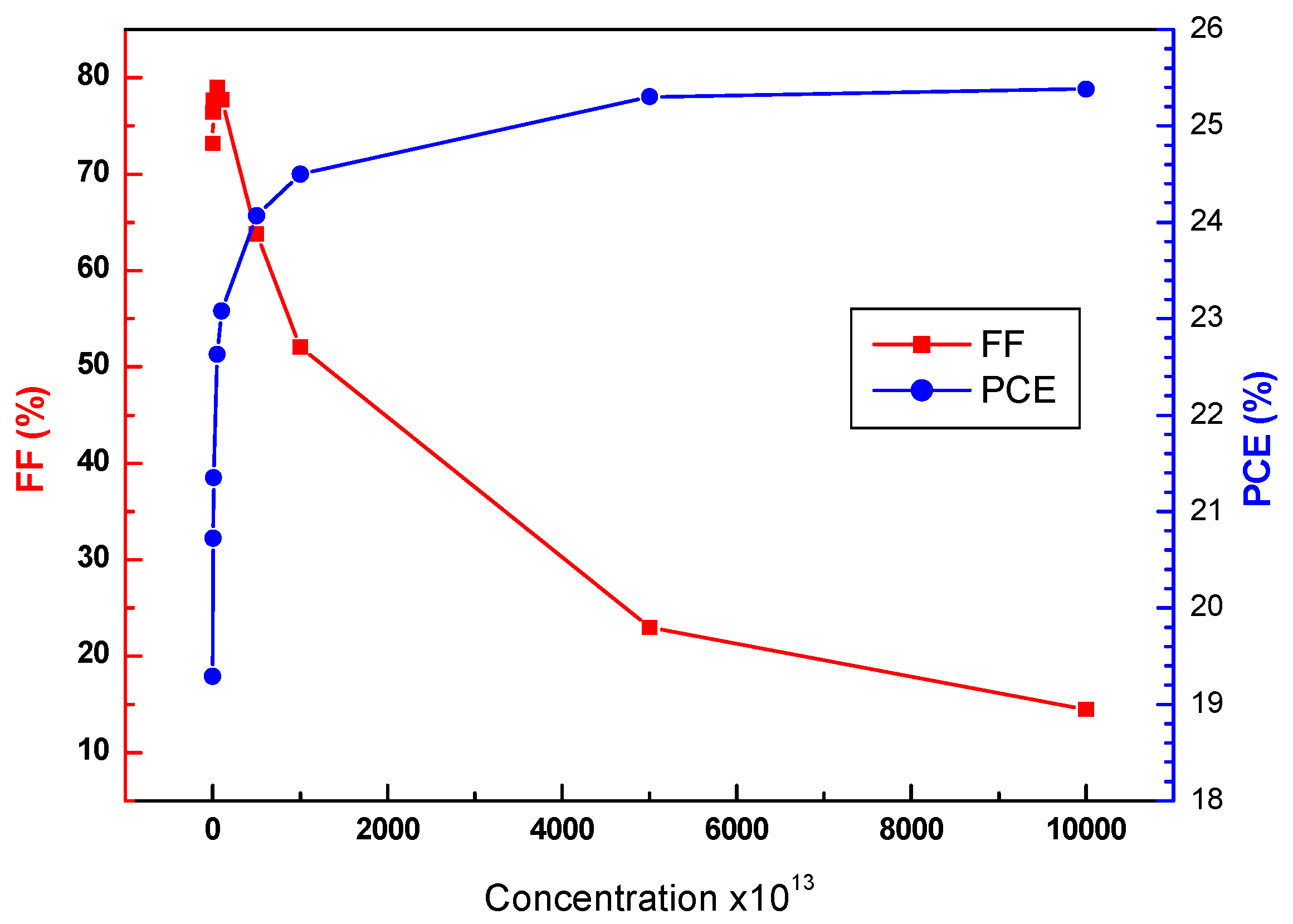
Figure 5: Variation of PCE and FF as a function of doping concentration NA of the SnS layer.
This is indicative of stronger recombination and resistive losses that will already be attacking the quality of the junction long before dimensions anywhere near those found in more heavily doped material are reached [13]. On the other hand, PCE is improved greatly by doping. It rises steadily from about 12% at 1014 cm−3 and gets very close to 25% at 1017 cm−3 (Fig. 5). This improvement is driven primarily by a strong increase of Voc, as already noticed above while Jsc remains almost constant-or perhaps somewhat reduced.
3.3 Optimization of the Solar Cell Efficiency
The thickness and doping concentration of the SnS absorbing layer strongly control light absorption, carrier collection and recombination. Thicker films increase optical absorption and Jsc up to a point, but also raise bulk recombination and series resistance, which degrades Voc and FF; conversely, ultra-thin films reduce absorption and Jsc despite improving collection. Increasing doping raises built-in field and carrier extraction, improving Voc and Jsc until Auger and trap-assisted recombination dominate, which lowers FF and efficiency.
In our ZnO/CdS/SnS architecture the combined effects limit power conversion efficiency to about 24.5% with a fill factor near 75%. To overcome these trade-offs, fragmenting the SnS absorber into multiple sub-layers with a linear gradient of charge concentration (lower near junction, higher towards back contact) can spatially tailor the electric field, enhance carrier separation, reduce recombination in deep regions, and permit thicker optical path length without sacrificing collection potentially increasing Jsc and preserving FF significantly. Table 2, summarize the characteristics of the absorber SnS sublayers.
Table 2: Summarizes the characteristics of the absorbent sublayers.
| Parameters | SnS-1 | SnS-2 | SnS-3 |
|---|---|---|---|
| Eg (eV) | 1.1 | 1.2 | 1.3 |
| Χ (eV) | 4.1 | 4.1 | 4.1 |
| εr | 13 | 13 | 13 |
| Nc (cm−3) | 1.8 × 10¹⁸ | 1.8 × 10¹⁸ | 1.8 × 10¹⁸ |
| Nv (cm−3) | 4.76 × 10¹⁸ | 4.76 × 10¹⁸ | 4.76 × 10¹⁸ |
| μn (cm2/V·s) | 15 | 15 | 15 |
| μp (cm2/V·s) | 100 | 100 | 100 |
| NA (cm−3) Grading linear distribution | 1013–1014 | 1014–1015 | 1015–1016 |
Fig. 6 shows the diagram energy band of the ZnO/CdS/SnS solar cell. As shown, a stepwise alignment through the different layers. The conduction band minimum of ZnO lies around 3.3 eV, while CdS is slightly lower at 2.42 eV, forming a favorable electron transport path. The SnS absorber is divided into three graded sublayers SnS-1, SnS-2 and SnS-3. This linear band gap grading produces a gradual downward shift in the conduction and valence bands, creating a built-in field that supports efficient carrier transport.
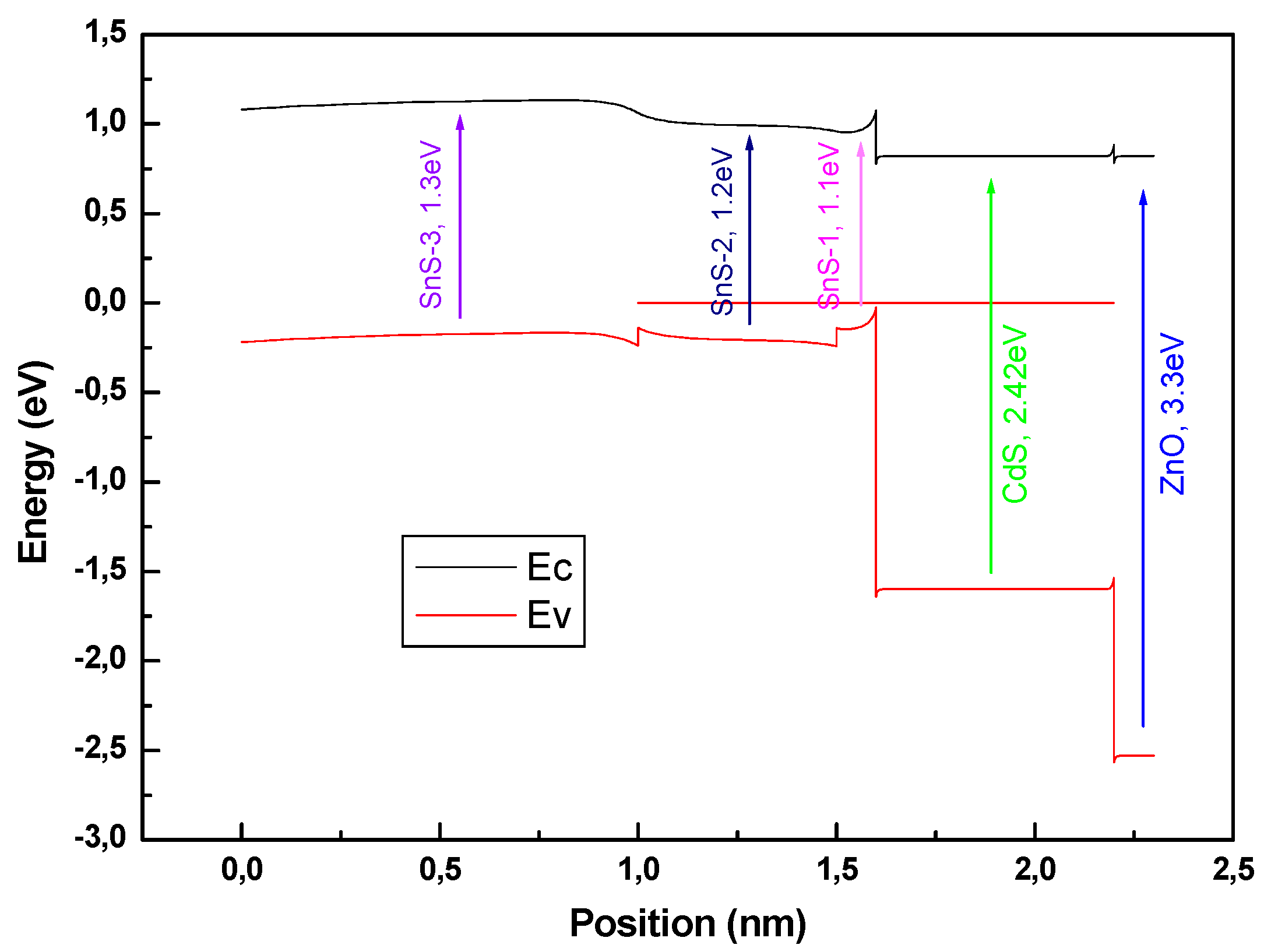
Figure 6: Diagram energy band of the optimized of SnS based solar cell.
The initial single-absorber ZnO/CdS/SnS structure yields baseline power conversion efficiency (PCE) of 24.5%. This relatively modest performance is primarily limited by incomplete optical absorption in the thin absorber and by carrier recombination at the rear interface. To address these limitations, the absorber was re-engineered into three sublayers (SnS-1, SnS-2, and SnS-3) with progressively increasing bandgaps of 1.10, 1.20, and 1.30 eV, respectively. A linear gradient of charge distribution was introduced across the absorber thickness to facilitate efficient carrier transport. The thickness of each sublayer was varied independently while the others were fixed, in order to evaluate the contributions of each region to device performance.
The effects of sublayer thickness on (Voc, Jsc) and (FF, PCE) are depicted in Fig. 7 and Fig. 8 respectively. As seen in Fig. 7, a notable improvement in photocurrent density is observed in the thickness range of 100–500 nm, which corresponds to the variation of SnS-1 at the device’s (SnS/CdS) interface. The Jsc current density increases from approximately 38.67 mA·cm−2 to 41.85 mA·cm−2 as SnS-1 is thickened, while the open-circuit voltage (Voc) rises from 0.8498 V to slightly above 0.8519 V. This increase is attributed to enhanced absorption of near-band-edge photons by the low bandgap (1.10 eV) SnS-1 layer, which directly converts incident photons at the front interface into carriers [14]. Owing to the internal electric field that the graded charge distribution maintains, the fill factor (FF) stays constant at 86.6%, which minimizes resistive losses. The PCE correspondingly rises from 28.5% to values approaching 30%, demonstrating that even modest thickening of the front sublayer provides a marked enhancement compared to the baseline single-layer structure.
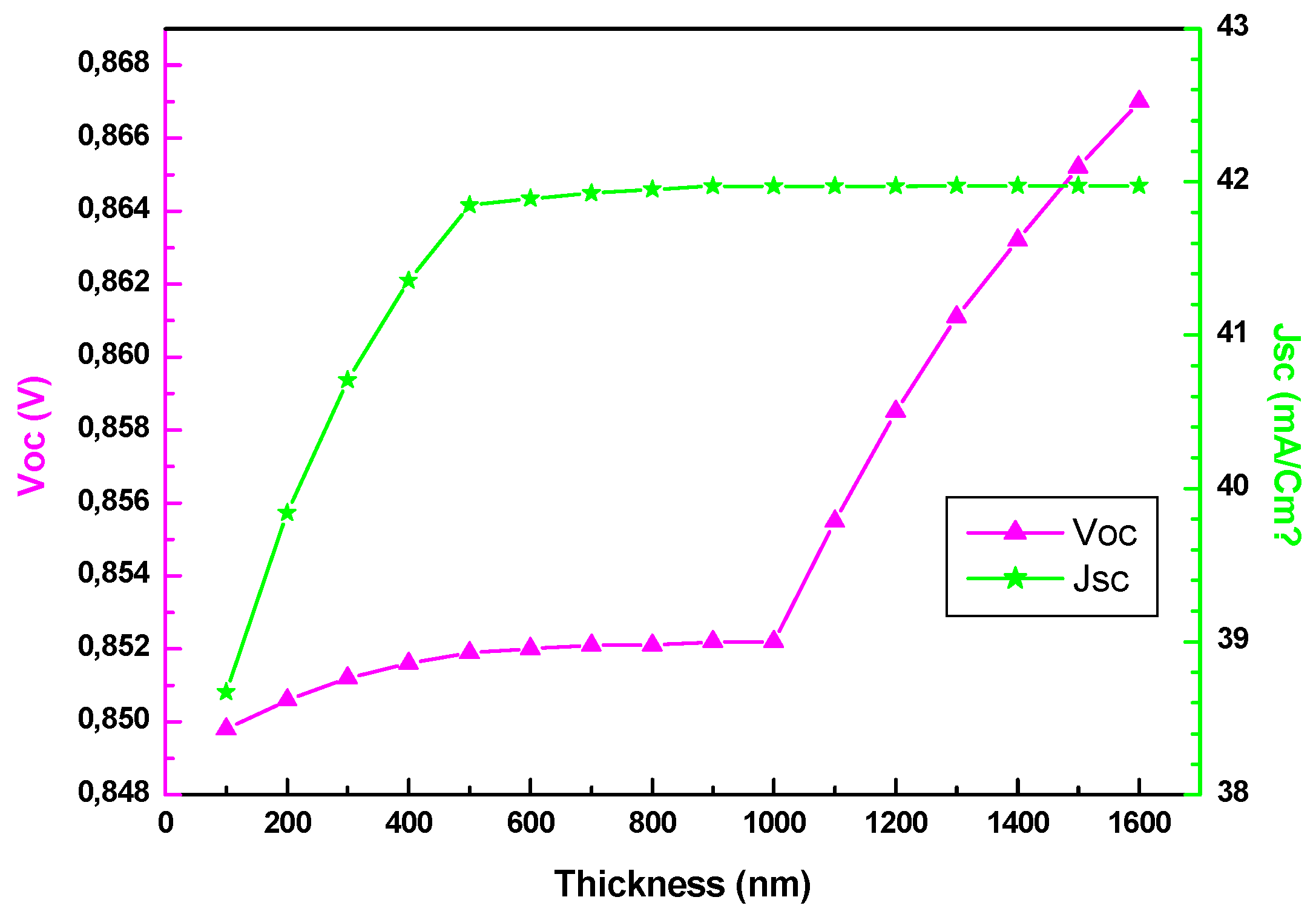
Figure 7: Effect of the sublayer thickness (SnS-1: 100–500 nm; SnS-2: 500–900 nm; SnS-3: 1000–1600 nm) on the Voc voltage Voc and the Jsc current Jsc.
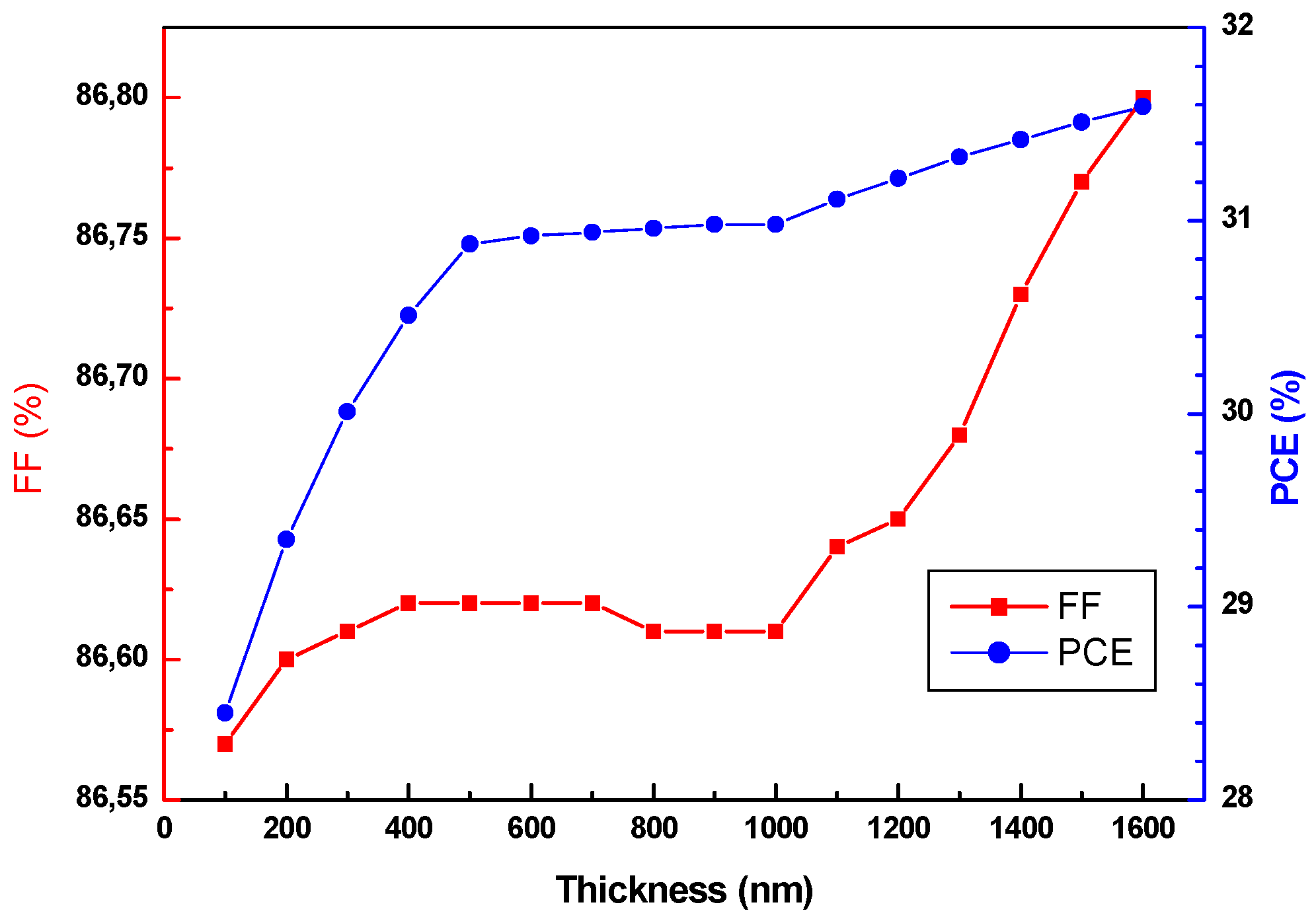
Figure 8: Effect of the sublayer thickness (SnS-1: 100–500 nm; SnS-2: 500–900 nm; SnS-3: 1000–1600 nm) on the FF and PCE.
When the intermediate sublayer SnS-2 is varied between 500 and 1000 nm, with SnS-1 and SnS-3 fixed at 500 and 1000 nm, respectively, further improvements are achieved. Jsc continues to rise, though at a slower rate, reaching values of 41.847–41.972 mA·cm−2. This sublayer, with a bandgap of 1.20 eV, absorbs higher energy photons that penetrate beyond SnS-1, thereby complementing the optical absorption spectrum. Voc increases gradually within this range, attaining values between 0.8819 and 0.8522 V, reflecting reduced recombination losses in the bulk absorber due to the graded bandgap structure [15]. FF remains nearly unchanged (86.62%), reinforcing the role of the linear charge distribution in sustaining efficient carrier extraction. As a result, the PCE steadily climbs beyond 30%, approaching 31% as SnS-2 thickness nears 1000 nm. This demonstrates the importance of a sufficiently thick intermediate layer to capture transmitted photons without compromising charge transport.
Finally, extending the rear sublayer SnS-3 from 1000 to 1600 nm produces the highest overall device efficiency. Jsc saturates at approximately 41.97 mA·cm−2, indicating that nearly complete absorption of the useful solar spectrum has been achieved. The most notable improvement in this range is observed in Voc, which increases to 0.867 V. This enhancement is attributed to the wide bandgap (1.30 eV) of SnS-3, which acts as a back-surface field, suppressing carrier recombination at the rear contact and reflecting minority carriers toward the junction [16]. The FF remains high and stable at 86.6%, demonstrating the robustness of carrier collection despite the increased total absorber thickness. The combined effects yield a peak PCE of 31.5% at the thickest SnS-3 configuration.
Overall, the transition from the baseline single layer ZnO/CdS/SnS architecture (24.5% PCE) to the optimized three sublayer structure (31.5% PCE) corresponds to an absolute improvement of 7.0 percentage points and a relative efficiency gain of approximately 28.6%. The introduction of a graded bandgap profile and linear charge distribution enhances both optical absorption and electronic quality of the absorber. The front and intermediate sublayers contribute primarily through increased photocurrent generation, while the rear sublayer suppresses recombination and improves Voc. The consistently high FF across all configurations confirms the effectiveness of the gradient in maintaining favorable internal electric fields. This combination optimization shows how bandgap-engineered, charge-graded absorbers can greatly enhance SnS-based solar cells’ performance.
This study investigates the efficiency of ZnO/CdS/SnS solar cell optimization through 1D SCAPS simulation. The findings indicate that, with a fill factor (FF) of 75%, the typical base cell’s power conversion efficiency (PCE) is limited to 24.5%. This limitation is attributed to the use of a single absorber layer, which led to incomplete absorption and recombination losses. The optimization of the PCE is adopted by splitting the absorber into sublayers with graded bandgap energy of 1.1, 1.2, and 1.3 eV and linearly grading carrier distribution. As a results, the improvement of near-band-edge absorption by bulk recombination suppressing, thereby enhance charge separation. Subsequently, solar cell efficiency increased from 24.5% to 28.45%, with a simultaneous improvement in fill factor from 75% to 86%. Additional optimization of sublayer thicknesses boosted the power conversion efficiency (PCE) to 31.5%, whereas the fill factor (FF) had a slight rise, reaching approximately 86.6%. The results indicate that integrating graded bandgap with thickness modulation and grading charge distribution is an effective approach to exceed the traditional performance limits of ZnO/CdS/SnS solar cells.
Acknowledgement:
Funding Statement: The authors received no specific funding for this study.
Author Contributions: The authors confirm contribution to the paper as follows: Conceptualization, Abdelhak Nouri, Djohra Dekhil and Abla Guechi; methodology, Abdelhak Nouri; software, Abla Guechi and Djohra Dekhil; validation, Abdelhak Nouri, Djohra Dekhil and Abla Guechi; investigation, Djohra Dekhil and Abla Guechi; writing—original draft preparation, Djohra Dekhil and Abla Guechi; writing—review and editing, Abdelhak Nouri. All authors reviewed and approved the final version of the manuscript.
Availability of Data and Materials: The authors confirm that the data supporting the findings of this study are available within the article.
Ethics Approval: Not applicable.
Conflicts of Interest: The authors declare no conflicts of interest.
References
1. Green MA, Dunlop ED, Hohl-Ebinger J, Yoshita M, Kopidakis N, Hao X. Solar cell efficiency tables (version 56). Prog Photovolt. 2020;28(7):629–38. doi:10.1002/pip.3303. [Google Scholar] [CrossRef]
2. Ramakrishna Reddy KT, Koteswara Reddy N, Miles RW. Photovoltaic properties of SnS based solar cells. Sol Energy Mater Sol Cells. 2006;90(18–19):3041–6. doi:10.1016/j.solmat.2006.06.012. [Google Scholar] [CrossRef]
3. Haass SG, Andres C, Figi R. Evaporated SnS thin films for solar cells: a review. IEEE J Photovolt. 2015;5:1287–93. doi:10.1109/JPHOTOV.2015.2448585. [Google Scholar] [CrossRef]
4. Di Mare S, Menossi D, Salavei A, Artegiani E, Piccinelli F, Kumar A, et al. SnS thin film solar cells: perspectives and limitations. Coatings. 2017;7(2):34. doi:10.3390/coatings7020034. [Google Scholar] [CrossRef]
5. Umar A, Tiwari P, Sadanand, Srivastava V, Lohia P, Dwivedi DK, et al. Modeling and simulation of tin sulfide (SnS)-based solar cell using ZnO as transparent conductive oxide (TCO) and NiO as hole transport layer (HTL). Micromachines. 2022;13(12):2073. doi:10.3390/mi13122073. [Google Scholar] [CrossRef]
6. Garain R, Basak A, Singh UP. Study of thickness and temperature dependence on the performance of SnS based solar cell by SCAPS-1D. Mater Today Proc. 2021;39:1833–7. doi:10.1016/j.matpr.2020.06.185. [Google Scholar] [CrossRef]
7. Peng CH, Lin YC. SCAPS-1D simulation of various hole transport layers’ impact on CsPbI2Br perovskite solar cells under indoor low-light conditions. Solids. 2025;6(3):31. doi:10.3390/solids6030031. [Google Scholar] [CrossRef]
8. Ait Abdelkadir A, Oublal E, Sahal M, Gibaud A. Numerical simulation and optimization of n-Al-ZnO/n-CdS/p-CZTSe/p-NiO (HTL)/Mo solar cell system using SCAPS-1D. Results Opt. 2022;8:100257. doi:10.1016/j.rio.2022.100257. [Google Scholar] [CrossRef]
9. Boubakri A, Jouidri A, Koumya Y, Rajira A, Almaggoussi A, Abounadi A. An output characteristics simulation of SnS based solar cells. Mater Today Proc. 2022;51:2047–52. doi:10.1016/j.matpr.2021.07.428. [Google Scholar] [CrossRef]
10. Dekhil D, Guessas H, Nouri A, Ullah S. Annealing effect on the photocurrent response of SnS thin films prepared by the chemical spray pyrolysis method. Chalcogenide Lett. 2023;20(8):549–58. doi:10.15251/CL.2023.208.549. [Google Scholar] [CrossRef]
11. Ramakrishna Reddy KT, Nwofe PA, Miles RW. Determination of the minority carrier diffusion length of SnS using electro-optical measurements. Electron Mater Lett. 2013;9(3):363–6. doi:10.1007/s13391-013-2194-3. [Google Scholar] [CrossRef]
12. Isha A, Kowsar A, Kuddus A, Hossain MK, Ali MH, Haque MD, et al. High efficiency Cu2MnSnS4 thin film solar cells with SnS BSF and CdS ETL layers: a numerical simulation. Heliyon. 2023;9(5):e15716. doi:10.1016/j.heliyon.2023.e15716. [Google Scholar] [CrossRef]
13. Jaramillo R, Sher MJ, Ofori-Okai BK, Steinmann V, Yang C, Hartman K, et al. Transient terahertz photoconductivity measurements of minority-carrier lifetime in tin sulfide thin films: advanced metrology for an early stage photovoltaic material. J Appl Phys. 2016;119(3):035101. doi:10.1063/1.4940157. [Google Scholar] [CrossRef]
14. Suzuki I, Kawanishi S, Omata T, Yanagi H. Current status of n-type SnS: paving the way for SnS homojunction solar cells. J Phys Energy. 2022;4(4):042002. doi:10.1088/2515-7655/ac86a1. [Google Scholar] [CrossRef]
15. Sharma I, Pawar PS, Kumar Yadav R, Nandi R, Heo J. Review on bandgap engineering in metal-chalcogenide absorber layer via grading: a trend in thin-film solar cells. Sol Energy. 2022;246:152–80. doi:10.1016/j.solener.2022.09.046. [Google Scholar] [CrossRef]
16. Benabbas S, Rouabah Z, Bouarissa N, Chelali N. The role of back surface field SnS layer in improvement of efficiency of CdTe thin film solar cells. Optik. 2016;127(15):6210–7. doi:10.1016/j.ijleo.2016.04.050. [Google Scholar] [CrossRef]
Cite This Article
 Copyright © 2026 The Author(s). Published by Tech Science Press.
This work is licensed under a Creative Commons Attribution 4.0 International License , which permits unrestricted use, distribution, and reproduction in any medium, provided the original work is properly cited.
 Downloads
 Citation Tools