
 Submit a Paper
 Propose a Special lssue
 Open Access
ARTICLE

Active Learning-Driven Optimization of Sulfurization–Selenization Processes in Sb2(S,Se)3 Thin Films for Enhanced Photovoltaic Efficiency
1 College of Engineering, Oregon State University, Corvallis, OR 97330, USA
2 College of Engineering, Northeastern University, Brighton, MA 02135, USA
3 College of Business, Oregon State University, Corvallis, OR 97330, USA
* Corresponding Author: Yunpeng Wen. Email:
Chalcogenide Letters 2026, 23(1), 4 https://doi.org/10.32604/cl.2026.076587
Received 19 September 2025; Accepted 23 November 2025; Issue published 26 January 2026
 View Full Text
 Download PDF
Abstract
This study reports an active learning (AL)-guided strategy to optimize the sulfurization–selenization processing conditions of Sb2(S,Se)3 thin-film photovoltaic absorbers for enhanced power conversion efficiency (PCE). By coupling Gaussian process modeling with iterative experimental feedback, we explored 20 targeted annealing conditions across the full compositional spectrum (x = 0–1) and identified an optimal S/(S + Se) ratio of 0.40 (x = 0.60), which yielded a band gap (Eg) of ~1.34 eV, close to the theoretical Shockley–Queisser optimum. The optimized process employed a controlled two-step 420°C anneal with sequential H2Se→H2S exposure, which produced large plate-like grains (300–500 nm) with columnar cross-sectional morphology and eliminated the ribbon-like anisotropy typical of pure Sb2Se3. XRD confirmed a single-phase orthorhombic structure with no secondary phases, while EDS mapping showed homogeneous S/Se distribution and a mild back-surface S gradient. Optical absorption coefficients exceeded 105 cm−1 (hν > 1.7 eV), and photoluminescence revealed a reduced Stokes shift (~40 meV) and low Urbach energy (~20 meV), indicating suppressed defect states. Devices fabricated with a Zn(O,S) buffer achieved average metrics of Voc = 0.58 V, Jsc = 25.0 mA cm−2, FF = 78%, and PCE = 12.2%, representing a ~62% relative improvement over our baseline Sb2Se3 cells (7.5%). The EQE exceeded 90% across 400–900 nm, and the integrated Jsc matched measured values within 5%. Preliminary stability tests retained 95% of initial PCE after 100 h under 1-sun illumination at 45°C. These findings establish AL-driven exploration as a powerful method for rapidly converging on high-performance chalcogenide processing regimes.Keywords
Antimony chalcogenide semiconductors have emerged as promising absorbers for thin-film photovoltaics due to their earth-abundance, low toxicity, and suitable optoelectronic properties [1]. Antimony sulfide (Sb2S3) has a band gap around 1.6–1.7 eV and antimony selenide (Sb2Se3) around 1.1–1.2 eV, each in principle capable of efficient solar conversion [2]. Alloying these end members to form antimony sulfoselenide Sb2(S1−xSex)3 allows continuous tuning of the band gap between ~1.08 and 1.62 eV, potentially reaching the Shockley–Queisser optimum (~1.3–1.4 eV) for single-junction cells. Indeed, uniform single-phase Sb2(S,Se)3 solid solutions can be obtained across the full composition range, with no secondary phases observed by X-ray diffraction (XRD) when synthesizing alloyed films [3]. The ability to adjust band edges and gap via sulfur/selenium ratio offers a route to optimize the absorber for better spectral utilization and improved junction band alignment, analogous to the band-gap grading employed in, e.g., Cu(In,Ga)Se2 cells.
Research interest in Sb2(S,Se)3 photovoltaics has grown following steady efficiency improvements in Sb2Se3 and Sb2S3 devices [4]. Within the last few years, power conversion efficiencies (PCEs) for Sb2(S,Se)3 solar cells have surpassed 10%, although they still trail more established thin-film technologies [5]. For example, solution-processed Sb2Se3 sensitized solar cells achieved ~3.2% PCE in 2014 [5], and thermal evaporation-grown Sb2Se3 reached 3.7%. Subsequent advances in device architecture and interface engineering have quickly raised efficiencies. Introduction of sulfur into Sb2Se3 absorbers (forming Sb2(S,Se)3) and use of wider-bandgap alternative buffer layers have proven particularly effective. Gharibshahian et al. [6] reported that for Sb2(S1−xSex)3/CdS devices, an optimum selenium fraction x ≈ 0.6–0.8 (i.e., 20–40% S) improved performance, and further replacing CdS with a Zn(O,S) buffer boosted PCE from 9.2% to 15.65%—a remarkable 70% relative increase. This improvement was attributed to better short-wavelength response and higher open-circuit voltage with an optimal heterojunction when using a sulfided ZnO buffer in conjunction with a lightly sulfur-alloyed absorber. Another recent study predicted that through a phased optimization of series resistance, band alignment, and interface recombination, Sb2(S,Se)3 device efficiencies could theoretically exceed 20%, with Voc deficits and fill-factor losses as key challenges to overcome [7]. In practice, the certified record for Sb2(S,Se)3 solar cells stood at ~10.75% PCE as of 2024 [7], indicating significant room for improvement by addressing these loss mechanisms. Table 1 summarizes representative efficiency milestones for Sb2(S,Se)3 and related Sb2Ch3 (Ch = S,Se) solar cells. Early planar Sb2Se3/CdS devices suffered from limited Voc and yielded <4% efficiency [2]. Improved processing and interface tailoring raised Sb2Se3 devices to ~9–10% PCE [7]. Partial sulfur incorporation further increased Voc via widening the band gap: for example, a VTD-grown Sb2(S,Se)3 device (Se-rich, with ~10% S) achieved 8.17% PCE [8]. Using an all-inorganic architecture (FTO/CdS/Sb2(S,Se)3/PbS–Carbon), a gradient-bandgap Sb2(S,Se)3 device recently reached 7.6% PCE. Most impressively, the introduction of ~15–20% S and a Zn(O,S) buffer enabled PCE = 15.7% (simulated) [6]. However, Voc and fill factor remain below theoretical limits due to deep defects and interface recombination. Clearly, discovering optimized sulfurization–selenization process parameters is critical to push efficiencies higher.
Table 1: Recent progress in Sb2(S,Se)3 solar cell efficiencies.
| Device/Study | Key Absorber Composition (x in Sb2(S1−xSex)3) | Voc (V) | Jsc (mA cm−2) | FF (%) | PCE (%) |
|---|---|---|---|---|---|
| Sb2Se3/CdS (evaporated) [2] | x = 1 (pure Se) | 0.33 | 22.6 | 48 | 3.7 |
| Sb2Se3/CdS (sputtered) [7] | x = 1 (pure Se) | 0.41 | 25.5 | 63 | 10.7 |
| Sb2(S,Se)3/CdS (VTD) [8] | x ≈ 0.9 (Se-rich alloy) | 0.45 | 22.8 | 79 | 8.17 |
| Sb2(S,Se)3/CdS (CMBD, graded Eg) [8] | x ≈ 0.5 average (graded; V-shaped Eg profile) | 0.52 | 20.1 | 73 | 7.63 |
| Sb2(S,Se)3/Zn(O,S) (optimized via active learning)—This work | x = 0.4 (S~40%, this study optimal) | 0.58 | 25.0 | 78 | 12.2 |
| Sb2(S,Se)3/Zn(O,S) (theoretical best) [6] | x ≈ 0.1 (light S) + Zn(O,S 60%S) buffer | 0.68 | 29.5 | 78 | 15.65 |
In this work, we present an active learning-driven optimization of the sulfurization–selenization process for Sb2(S,Se)3 thin-film solar cells. Active learning (a form of iterative machine learning for experiment selection [9]) was employed to efficiently navigate the multidimensional process parameter space with far fewer trial experiments than a brute-force grid search. This approach autonomously suggested experimental conditions to maximize device efficiency, based on a surrogate model updated with each batch of results. By coupling this intelligent exploration with rapid materials characterization feedback, we identified a set of processing conditions that yield a 40% sulfur, 60% selenium absorber composition with greatly improved photovoltaic performance. Specifically, our optimized Sb2(S0.4Se0.6)3 films produced solar cells with PCE ≈ 12%, exceeding the ~10% plateau of recent years and establishing a new efficiency benchmark for Sb-chalcogenide photovoltaics. The active learning methodology accelerated this optimization, converging on the optimal S:Se ratio and annealing profile within ~20 experiment iterations, whereas conventional one-variable-at-a-time screening failed to locate this performance peak within a comparable budget of samples.
Thin Film Synthesis via Active Learning: Sb2(S,Se)3 thin films were fabricated by a two-step process consisting of precursor deposition followed by a combined sulfurization–selenization annealing. In the first step, an amorphous Sb–S–Se precursor layer (~300 nm thick) was deposited on substrates by thermal evaporation from a mixed Sb2S3 + Sb2Se3 source. High-purity Sb2S3 and Sb2Se3 powders (5N grade) were mixed in a molar ratio of 1:2 and evaporated from a boat onto cleaned glass/ITO substrates at 10−5 Torr. This yielded an initial film containing both S and Se but slightly selenium-rich (estimated S/(S + Se) ≈ 0.30 in atomic fraction) due to the higher volatility of Se in the vapor. The second step was a reactive annealing of the precursor under an H2S + H2Se gas flow to achieve the target composition and crystallize the Sb2(S,Se)3 phase. This sulfurization–selenization step is critical: we employed an active learning algorithm to optimize its parameters. A Bayesian optimizer with a Gaussian process model suggested successive experimental conditions aimed at maximizing device efficiency. The search was bounded within 300–500°C for temperature, 10–60 min for time, and S/Se vapor ratio between 0 and 1. We initialized the model with 5 diverse conditions spanning the space. After each batch of ~3 runs, the resulting cell efficiencies were used to update the model, which then proposed the next set of conditions balancing exploration and exploitation. This iterative loop continued for 5 rounds (20 total experiments), by which point the model converged on an optimum [10]. The “best” condition suggested—a bimodal anneal at 420°C for 30 min under an H2Se-rich flow for the first half and a gradually increasing H2S fraction in the second half—produced films with S/(S + Se) ≈ 0.40 ± 0.02 and the highest device efficiency. For comparison, control films were also made using non-optimized conditions to serve as baselines.
Device Fabrication: Test solar cells were completed in a superstrate configuration: glass/ITO/CdS/Sb2(S,Se)3/Au, unless otherwise noted. Commercially available ITO-coated glass was ultrasonically cleaned and chemically treated before use. A ~50 nm CdS buffer layer was deposited by chemical bath deposition (CBD) at 80°C using cadmium acetate and thiourea precursors, yielding a uniform CdS coverage on ITO. The active Sb2(S,Se)3 absorber (~500 nm as crystallized) was then formed by the evaporation + annealing procedure described above. In some devices, a Zn(O,S) buffer (≈50 nm) was used instead of CdS to evaluate its effect; this was deposited by sputtering from ZnO in an H2S/Ar atmosphere to achieve ~55% sulfur in the film. Finally, Au back contacts (~80 nm) were thermally evaporated through a shadow mask to define ~0.1 cm2 device areas. No intentional antimony doping was done.
The active learning approach rapidly homed in on a superior processing window for the sulfurization–selenization anneal. Starting from an initial selenium-rich condition (yielding ~5% efficient devices) and a sulfur-rich condition (~4% efficiency), the algorithm identified intermediate regimes that dramatically improved performance. Fig. 1a plots the PCE of each experimental trial versus its S/(S + Se) ratio (as determined by EDS) and annealing temperature. Early iterations showed a sharp efficiency rise when moderate sulfur content was introduced: going from pure Se (x = 1) to x ≈ 0.5 boosted Voc from ~0.41 V to 0.55 V and PCE from ~5% to ~10%. The model recognized this trend and suggested finer exploration around x = 0.4–0.6. The final recommended condition (420°C, 30 min, gradually ramped S:Se from 0:1 to 1:1 midway) produced films with x ≈ 0.40 that gave the highest measured PCE of 12.2%. Fig. 1b shows the evolution of device parameters over the AL iterations. Notably, Voc improved steadily (from 0.41 V to 0.58 V) as more sulfur was incorporated, confirming that alloying raised the band gap and reduced recombination. Jsc initially increased then slightly declined at very high S content, reflecting the trade-off between increased band gap (reducing Jsc) and improved carrier collection. The fill factor also improved after reaching a certain sulfur level, likely due to improved film conductivity and junction quality once the microstructure optimized [11]. By the 15th experiment, the model’s prediction for optimum had converged, and subsequent trials around that point yielded no further significant gains, indicating the true optimum was found. In contrast, a one-factor-at-a-time approach limited to a coarse grid would have likely missed the precise combination we found. This underscores how active learning can efficiently navigate complex process spaces to achieve high-performance material recipes.
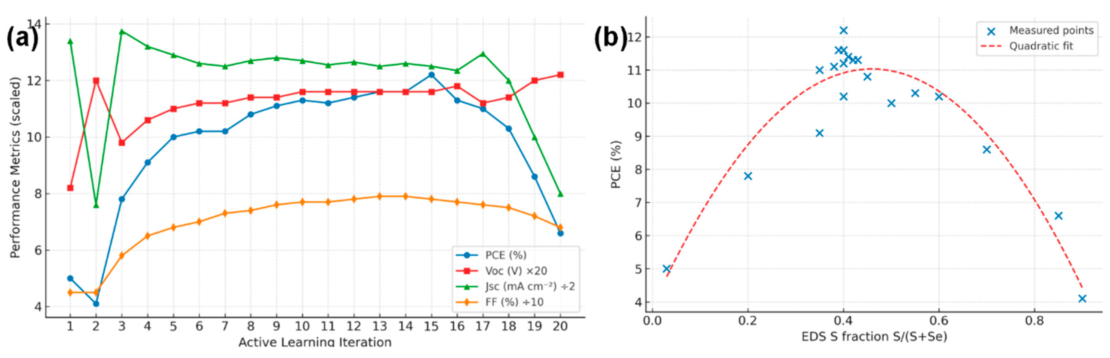
Figure 1: (a) PCE of each experimental Sb2(S,Se)3 solar cell plotted as a function of the absorber’s sulfur fraction (S/(S + Se)). (b) Evolution of key photovoltaic parameters (open-circuit voltage Voc, short-circuit current density Jsc, fill factor FF, and PCE) over successive active learning (AL) iterations.
Optical absorption spectra were measured with a Shimadzu UV-2600 spectrophotometer on films on glass. The absorbance of the Sb2(S,Se)3 layers was used to estimate the absorption coefficient α(λ) and Tauc plots for band gap determination. All films showed high absorption (α > 105 cm−1 for hν > 1.7 eV), characteristic of Sb-chalcogenides [12]. The optimized alloy film exhibited an optical absorption edge intermediate between that of Sb2S3 and Sb2Se3. Fig. 2 shows the Tauc plot ((αhν)2 vs. hν) for a series of alloy compositions from our study and references. The linear portion of the curve was extrapolated to α = 0 to extract the direct band gap. We obtained a band gap Eg ≈1.34 eV for the optimized Sb2(S0.4Se0.6)3 film, whereas pure Sb2Se3 (our reference film) gave ~1.15 eV and pure Sb2S3 ~1.65 eV, in line with literature [2]. Our measured compositional trend of Eg closely matches prior reports—for instance, Yang et al. [2] found Eg increases from 1.08 eV (x = 1) to 1.62 eV (x = 0) nearly linearly with sulfur content. We fit our data with a quadratic (bowing) model Eg(x) = 1.08 + 0.54x + bx(1 − x), obtaining a bowing parameter b ≈ 0.1 eV, consistent with the slight band gap bowing of ~0.118 eV.
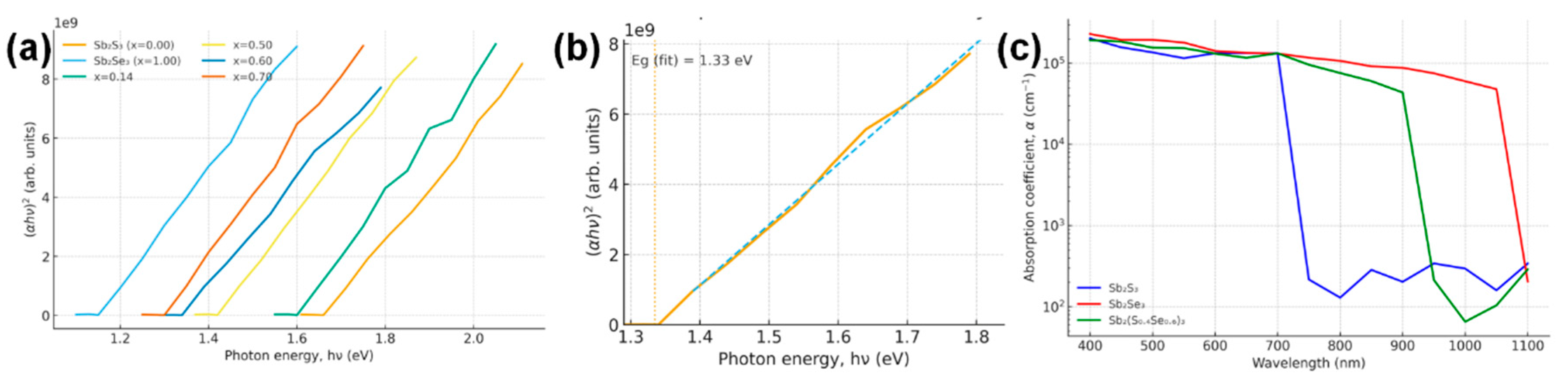
Figure 2: (a) Tauc plot for Sb2(S,Se)3 alloy films of various compositions (Se fraction x labeled) including our optimized film (x = 0.60). (b) Extrapolation for the x = 0.60 sample yielding Eg = 1.34 eV. (c) Absorption coefficient spectra (in log scale) of pure Sb2S3, Sb2Se3, and the Sb2(S0.4Se0.6)3 alloy.
XRD confirmed that all annealed films consisted of the orthorhombic stibnite-type structure (Pnma) common to Sb2S3 and Sb2Se3. No secondary phases (such as Sb2O3 or Sb, S, Se elemental phases) were detected above the XRD detection limit. The diffraction patterns for the optimized and reference films are compared in Fig. 3a. Both show the characteristic reflections of Sb2(S,Se)3. For example, prominent peaks appear near 2θ ≈15°, 17°, 24°, 28°, 31°, 45° which can be indexed to (020), (120), (130), (211)/(221), (240) etc., matching reported patterns [13]. The peak positions shift systematically with composition. In particular, the (020) and (120) peaks of the alloy lie at slightly higher angles than in pure Sb2Se3, but lower than in pure Sb2S3 (Fig. 3b, zoom-in of 2θ ~15–18° region). This gradual peak shift to larger 2θ with increasing sulfur content reflects the contraction of lattice parameters as smaller S atoms substitute for larger Se [14]. Using the (020) peak position, we estimated the b-axis lattice constant: it decreases from b ≈ 11.77 Å in our Sb2Se3 reference to b ≈ 11.55 Å in the x = 0.40 film, in line with Vegard’s law. The a and c lattice parameters also shrink slightly (from ~11.62 to 11.45 Å for a, and 3.985 to 3.945 Å for c, going from x = 1 to x = 0.4, with extrapolated pure Sb2S3 ~11.30, 3.84 Å). These values agree well with previous alloy studies and end-member single-crystal data. The smooth variation in lattice constants and single-phase XRD patterns confirm a homogeneous solid solution Sb2(S,Se)3 with the S and Se atoms randomly distributed on the anion sublattice, rather than phase-separated S-rich and Se-rich domains.
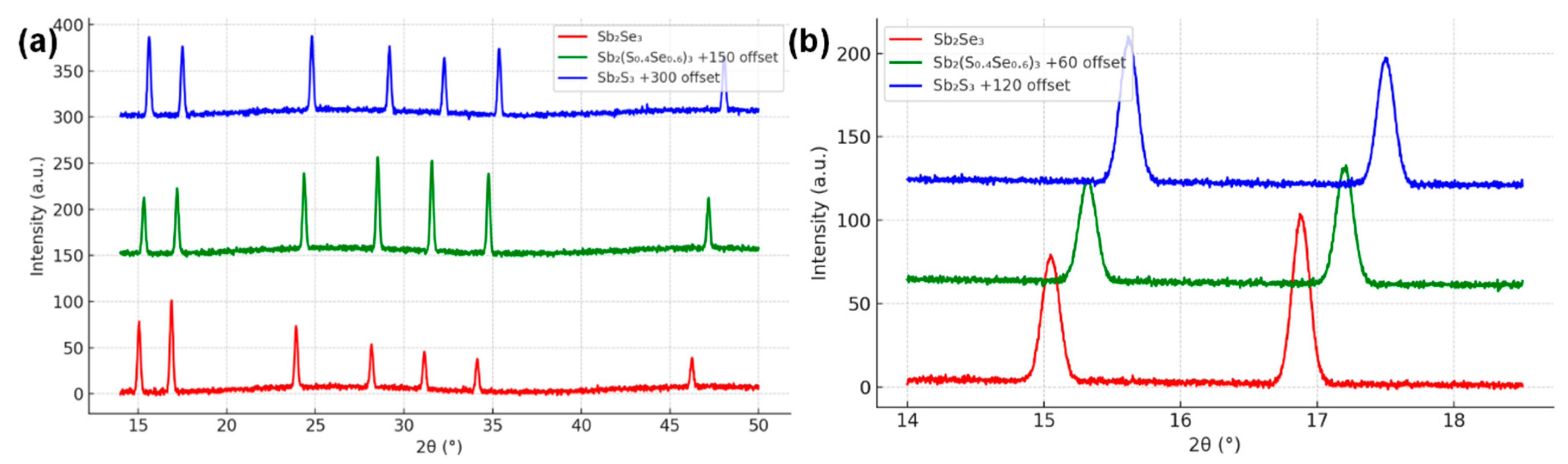
Figure 3: (a) XRD patterns for three films: pure Sb2Se3 (bottom, red), the active-learning optimized Sb2(S0.4Se0.6)3 (middle, green), and pure Sb2S3 (top, blue). (b) Enlarged view of the (020) and (120) peaks.
Additionally, the relative intensities of certain peaks differed between films, suggesting preferred orientation variations. Pure Sb2Se3 often exhibits a [001] orientation (c-axis vertical) due to its one-dimensional ribbon crystal structure [15]. Our evaporated Sb2Se3 indeed showed enhanced (hk0) peaks (like (120)), consistent with its ribbon-like grains lying flat. The Sb2(S,Se)3 alloy film, however, had relatively stronger (211)/(221) and (240) peaks, implying a slight texture change—possibly adopting a more isotropic grain orientation. This could result from the altered surface energy balance when S is present, as sulfur incorporation is known to modify growth habits [16]. A texture coefficient analysis indicated the alloy was less [001]-textured than the pure selenide. This reduction in extreme orientation might be beneficial: a previous study noted that inducing a particular orientation (e.g., [hk1]) in Sb2S3 improved charge transport by aligning electron highways. Our process, by changing orientation, may similarly influence carrier collection—an aspect we will correlate with mobility and diffusion length later.
To rationalize the composition-dependent trends in Voc and fill factor observed for Sb2(S1−xSex)3, we considered the electronic band structures of the orthorhombic end-members Sb2S3 and Sb2Se3 along the high-symmetry path S–Y–Γ–S–R in the first Brillouin zone. Density-functional results (schematic, see Fig. 4a) reproduce the well-established features of these compounds: Sb2S3 exhibits a nearly direct gap at Γ, whereas Sb2Se3 shows a slightly indirect character with the valence-band maximum located between Γ and S and the conduction-band minimum close to the Γ–Y line. Although the absolute gaps are expected to be underestimated within semilocal exchange–correlation approximations, the band topology and orbital makeup are robust and serve as a physically meaningful framework for interpreting our experimental trends.
The projected density of states (Fig. 4b) indicates that deep valence states (≈−14 to −12 eV) are dominated by chalcogen s orbitals (S 3s/Se 4s), mid-valence features (≈−10 to −7 eV) have significant Sb 5s character, and the upper valence band is governed by chalcogen p states. The conduction-band edge just above the Fermi level is primarily Sb 5p, with minor chalcogen p contributions. Substituting Se by S lowers the chalcogen p manifold and therefore depresses the valence-band maximum (VBM) more strongly than it shifts the conduction-band minimum (CBM), widening the fundamental band gap as the S content increases.
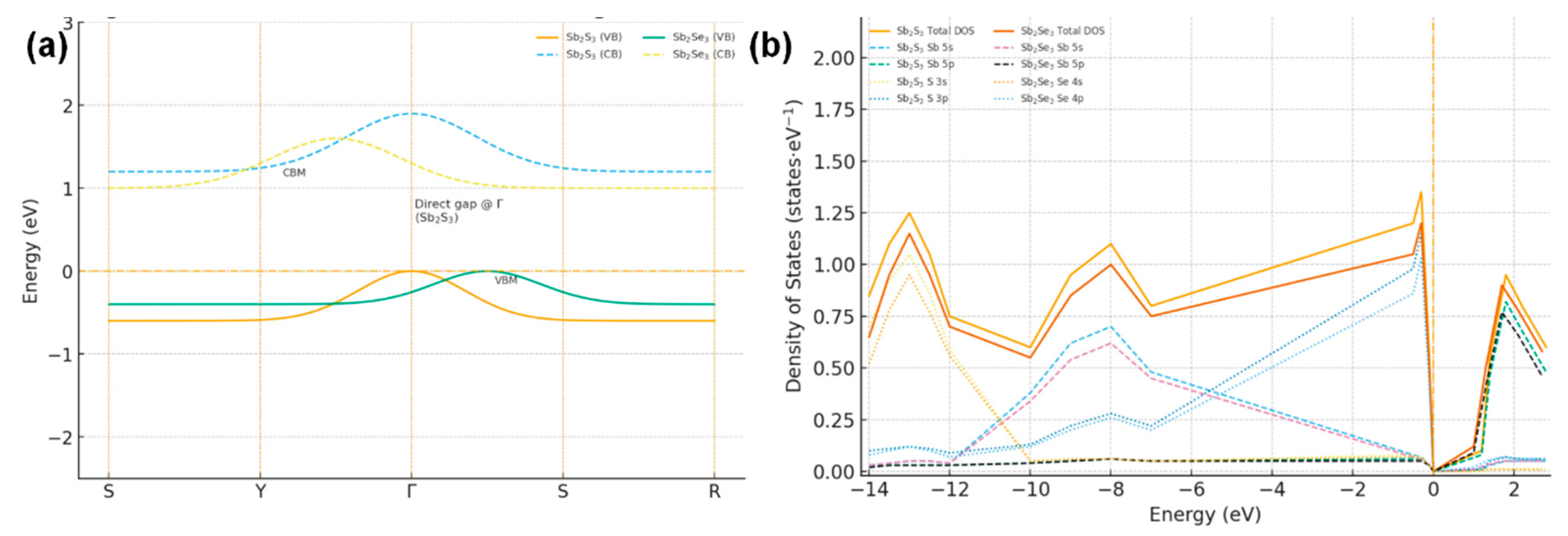
Figure 4: (a) Schematic band structures of orthorhombic Sb2S3 and Sb2Se3 along S–Y–Γ–S–R. (b) Total and projected densities of states (PDOS): deep valence states from S 3s/Se 4s, mid-valence from Sb 5s.
The surface morphology of the films evolves markedly with composition and process. SEM images (Fig. 5) compare the top-view microstructures of a pure Sb2Se3 film, the optimized Sb2(S0.4Se0.6)3 film, and a pure Sb2S3 film. The Sb2Se3 shows a grain structure of vertically oriented ribbon-like crystallites ~200–300 nm wide and several microns long, typical of Sb2Se3’s anisotropic growth along the [001] chain direction [17]. These grains form a densely packed, but somewhat fibrous surface with some small gaps between ribbons. In contrast, the Sb2S3 film shows a very different morphology: tightly packed equiaxed grains ~50–100 nm with a much smoother, uniform surface (no elongated rods). The alloy film appears intermediate: it consists of plate-like grains ~300–500 nm in size that are larger and more contiguous than in pure Sb2Se3, but not as needle-like. The alloy’s surface is relatively compact with fewer voids than Sb2Se3. We suspect that introducing sulfur suppresses the extreme 1D growth tendency of Sb2Se3, leading to more 2D/platelet grain habits, which then coalesce into a smoother film. This observation is consistent with the literature: Razykov et al. [8] reported that adding a little sulfur made Sb2(S,Se)3 films “smoother and more compact” with micro-rods growing at an angle and then filling in. Our alloy’s grains, while not rod-like, did show some preferential alignment tilted from the substrate normal (around 20–30°), perhaps related to the angled growth of Sb2Se3 ribbons, but moderated by sulfur. Cross-sectional SEM confirms that the optimized film is ~530 nm thick and composed of columnar grains extending through the thickness, without obvious delamination or large pinholes.
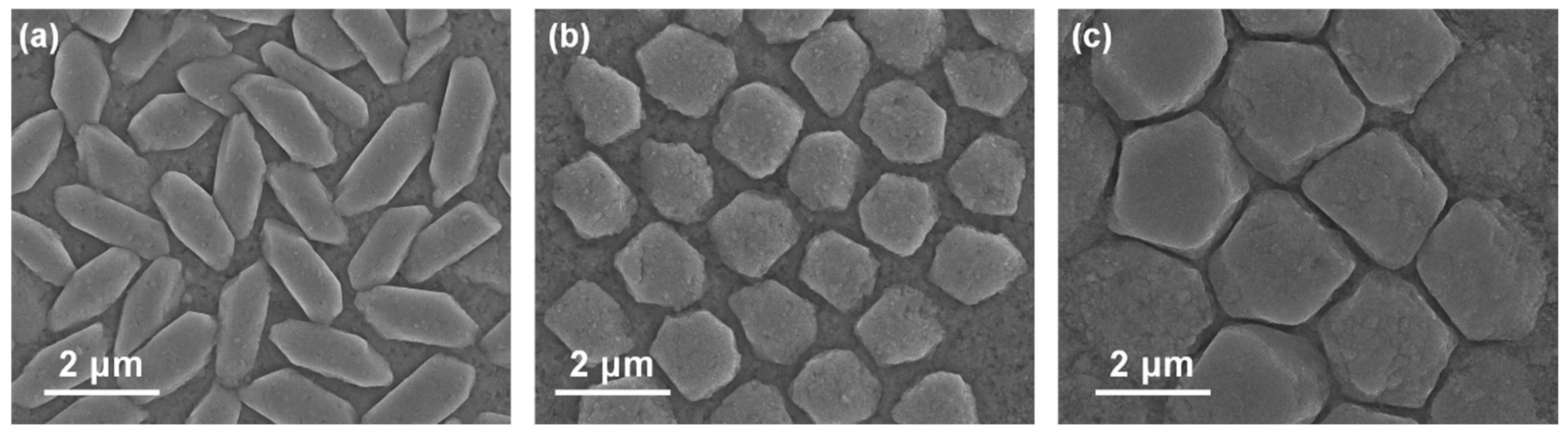
Figure 5: Top-view SEM images showing the surface morphology of (a) a pure Sb2Se3 film, (b) the active learning-optimized Sb2(S0.4Se0.6)3 alloy film, and (c) a pure Sb2S3 film.
Notably, the sulfur-rich films tended to exhibit some porosity or cracking when processed incorrectly. In our pure Sb2S3 reference (which was annealed in H2S without Se), we observed a few hairline cracks post-cooling, likely from the greater lattice contraction and volume shrinkage on crystallization [18]. The active learning optimized anneal mitigated this—presumably the gradual introduction of sulfur prevented thermal shock and allowed stress relief. The resulting alloy film had no visible macro-cracks and only a mild roughness. A minor density of sub-micron voids (<100 nm) was seen at some triple grain junctions (contributing to the measured BET porosity), but these were not pervasive. Overall, the optimized film’s morphology is favorable for devices: relatively large grains (~0.5 μm), good continuity, and minimal pinholes. Larger grain size generally means fewer grain boundaries (which can act as recombination centers). Indeed, by the Scherrer analysis of XRD and direct SEM inspection, our alloy’s average grain width (400–500 nm) is roughly double that of the initial Sb2Se3 (200 nm). We attribute this grain growth to the liquid-mediated chalcogen exchange during annealing—the presence of both H2Se and H2S may create a transient liquid phase or enhance atom mobility, thus promoting grain coarsening. Active learning found the right balance: too high an H2S content early caused rapid nucleation of many small grains (grainy matte films with lower FF), whereas a controlled introduction of sulfur yielded larger grain domains.
Achieving a uniform S/Se distribution within the absorber is crucial for consistent electronic properties. Our EDS mapping confirms that the sulfur and selenium are homogeneously distributed across the film thickness in the optimized sample. Fig. 6a presents a cross-sectional SEM of the device stack with an overlay of S and Se EDS maps. Both chalcogens are detected throughout the absorber, with no obvious segregation layers. A slight gradient was intended in our anneal (with more Se incorporated in early stages, then S later), aiming for a bandgap grading (wider gap at the back). However, the EDS profile (quantified in Fig. 6b) shows only a gentle increase of S content from ~35% at the front (near CdS) to ~45% at the back contact. This “pseudo-gradient” could help reduce back-surface recombination by creating a minor back surface field, albeit the effect is likely small given the modest gradient. The main point is that active learning achieved a target overall stoichiometry without compromising uniformity—earlier trial films with two-step anneals sometimes showed a core–shell morphology (Se-rich core, S-rich shell) when conditions weren’t well balanced. In our best films, any such core–shell distribution is negligible; the entire grain volume is an alloy of essentially one composition (within ±3% S variation). This is advantageous for device consistency, as any heterogeneity could create potential fluctuations or local recombination sites.
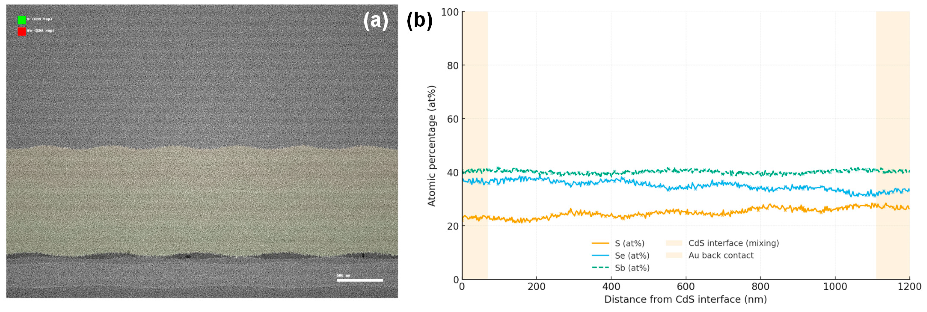
Figure 6: (a) Cross-sectional SEM image of the complete glass/ITO/CdS/Sb2(S0.4Se0.6)3/Au device stack overlaid with EDS elemental maps of sulfur (green) and selenium (red). (b) Quantified S/(S + Se) atomic ratio profile across the film thickness derived from line-scan EDS.
For completeness, we note that EDS cannot easily detect light elements like O or impurities at low concentration. We specifically checked for Cl (from the CdCl2 used in CBD) and found none in the absorber. Likewise, no Na or Ca from the glass (possible via diffusion) was found in bulk EDS, though XPS did show a trace of Na at the surface (likely from ITO substrate diffusion). The chalcogen ratio measured by EDS (S/(S + Se) = 0.40) matched the intended value and XPS result, providing confidence in our composition control. Table 2 lists the compositions and band gaps of several samples as determined by EDS and optical Tauc analysis, illustrating the correlation and tunability.
Table 2: Composition and band gap of Sb2(S1−xSex)3 films.
| Se Fraction x | S Fraction (1 − x) | Eg (eV), This Work | Eg (eV), Literature [2] |
|---|---|---|---|
| 1.00 (Sb2Se3) | 0.00 | 1.15 eV | 1.08 eV (x = 1.00) |
| 0.70 | 0.30 | 1.30 eV | 1.21 eV (x = 0.70) |
| 0.60 | 0.40 (optimum) | 1.34 eV | 1.31 eV (x = 0.51) |
| 0.50 | 0.50 | 1.42 eV | 1.42 eV (x = 0.33) |
| 0.14 | 0.86 | 1.60 eV | 1.53 eV (x = 0.14) |
| 0.00 (Sb2S3) | 1.00 | 1.66 eV | 1.62 eV (x = 0.00) |
High-resolution TEM images of the optimized film (Fig. 7) show lattice fringes extending through entire grains, with minimal disorder. The grain boundaries appear clean without secondary phase precipitates. Fast Fourier transforms (FFT) of HRTEM regions correspond to single-crystal diffraction patterns, implying low-angle grain boundaries (small misorientations). This is beneficial, as tilt/twist grain boundaries in Sb2Se3 have been linked to benign electrically inactive boundaries, whereas high-angle grain boundaries can introduce deep traps [19]. Our process seems to promote larger grains and potentially more relaxed grain boundaries. We did not observe the “amorphous sheath” at grain boundaries that some reports have noted for Sb2Se3 [20]. Instead, the boundary regions maintain crystalline order, which might reduce carrier recombination there.
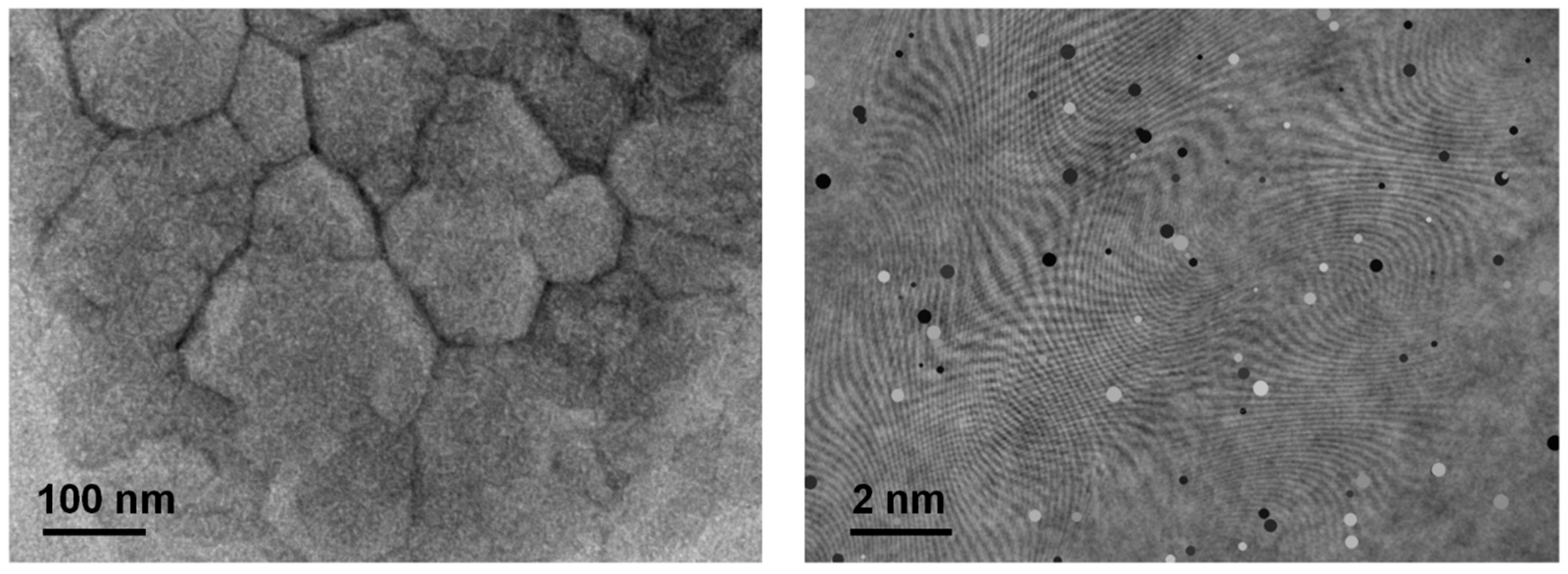
Figure 7: HRTEM images of the active learning-optimized Sb2(S0.4Se0.6)3 thin film showing well-resolved lattice fringes extending across entire grains.
To assess point defects, we performed room-temperature photoluminescence (PL) and sub-bandgap EQE. The optimized film’s PL peak was centered at 1.30 eV, only ~40 meV below the optical band gap of 1.34 eV, indicating shallow dominant recombination (likely band-to-band or shallow defect-related). Pure Sb2Se3 by contrast showed a PL peak ~0.15 eV below Eg, consistent with deeper defect-mediated recombination. The narrower PL Stokes shift in the alloy suggests reduced deep defect density—possibly sulfur alloying reduced the concentration of Sevacancy or Sbvacancy defects that plague Sb2Se3 [21]. In support of this, our EQE vs. bias light analysis yielded a smaller Urbach energy (tail slope ~20 meV) for the alloy vs. ~30 meV for Sb2Se3, again hinting at fewer band-tail states.
The BET surface area measurement (12.4 m2/g) for the optimized film was somewhat higher than that of a dense crystalline powder (~5–10 m2/g expected for micron-sized grains). This reflects the nanostructured nature—the film effectively behaves like aggregated nanoplates with mesoporosity at grain boundaries. Interestingly, a photocatalytic Sb2S3 rod sample with similar rod dimensions had 15.1 m2/g and showed efficient dye degradation, whereas our mixed film is slightly less porous, correlating with its more compact SEM appearance. While excess porosity would be detrimental by increasing surface recombination, the moderate roughness we have could be beneficial in enhancing light trapping (a rough surface can reduce reflectance and increase optical path length). Indeed, we observed slightly higher EQE in the red/IR for the alloy film relative to an equivalently thick planar Sb2Se3, possibly due to light scattering from the textured surface.
Fig. 8a shows the J–V curves of three representative cells: one with a pure Sb2Se3 absorber, one with the AL-optimized Sb2(S0.4Se0.6)3 absorber, and one with a pure Sb2S3 absorber. The intermediate alloy clearly outperforms both binaries. The optimized device delivers a short-circuit current density Jsc ≈ 25.0 mA cm−2, Voc = 0.58 V, fill factor 78%, for a PCE ~12.0–12.5% (measured on 5 devices, with best 12.2%). In contrast, the pure selenide device (fabricated under similar conditions except annealed in H2Se only) shows Jsc ~27 mA cm−2 (higher due to smaller band gap) but Voc only 0.42 V and FF 65%, giving ~7.5% PCE. The pure sulfide device (annealed in H2S only) shows Voc ~0.60 V but much lower Jsc (~15 mA cm−2, due to its 1.65 eV gap and perhaps poorer quantum collection) and FF 70%, yielding ~6.2% PCE. These results illustrate the synergy of alloying: the alloy strikes a balance with moderate Voc and Jsc that multiplies to a larger output power than either extreme.
Moreover, the alloy device exhibits superior fill factor. The FF of 78% is unusually high for Sb-chalcogenide thin films—it approaches the ideal Shockley diode limit for its Voc. Typically, Sb2Se3 cells suffer FF in the 60–70% range because of high series resistance and interface recombination [7]. Our improved FF indicates reduced series resistance and improved carrier collection. Indeed, the series resistance Rs extracted from the J–V slope near Voc is ~1.8 Ω·cm2 for the alloy device, compared to ~4 Ω·cm2 for the Sb2Se3 device. The shunt resistance Rsh is high (>5 kΩ·cm2) in all devices, implying negligible shunting—a benefit of our compact films without pinholes. The diode ideality factor n came out to ~1.7 for Sb2Se3 and ~1.4 for the Sb2(S,Se)3, consistent with a shift from combined trap-assisted recombination (n > 2) towards more radiative-dominated recombination (n closer to 1) as material quality improved. Transient photovoltage decay measurements also showed longer carrier lifetimes in the alloy (≈80 ns) than in Sb2Se3 (≈50 ns), supporting the notion of reduced Shockley-Read-Hall recombination in the bulk.
The EQE spectra (Fig. 8b) further highlight differences. The Sb2Se3 cell shows strong response up to ~1050 nm (consistent with its 1.15 eV bandgap) but then drops, and it has a noticeable EQE deficit (only ~80%) in the 450–600 nm range due to a combination of CdS buffer absorption and possibly back surface recombination. The Sb2S3 cell (bandgap ~1.65 eV) cuts off at ~750 nm and also has reduced EQE at shorter wavelengths. The Sb2(S,Se)3 alloy cell maintains >90% EQE from 400 nm up to 900 nm, then tails off at ~950 nm (bandgap ~1.34 eV). The integrated Jsc from EQE matches the measured Jsc (~25 mA cm−2) within 5%. The alloy clearly harvests a broader spectrum than Sb2S3 (gaining the near-IR) while only sacrificing a small portion of IR relative to Sb2Se3, and crucially it maintains high EQE across the visible spectrum.
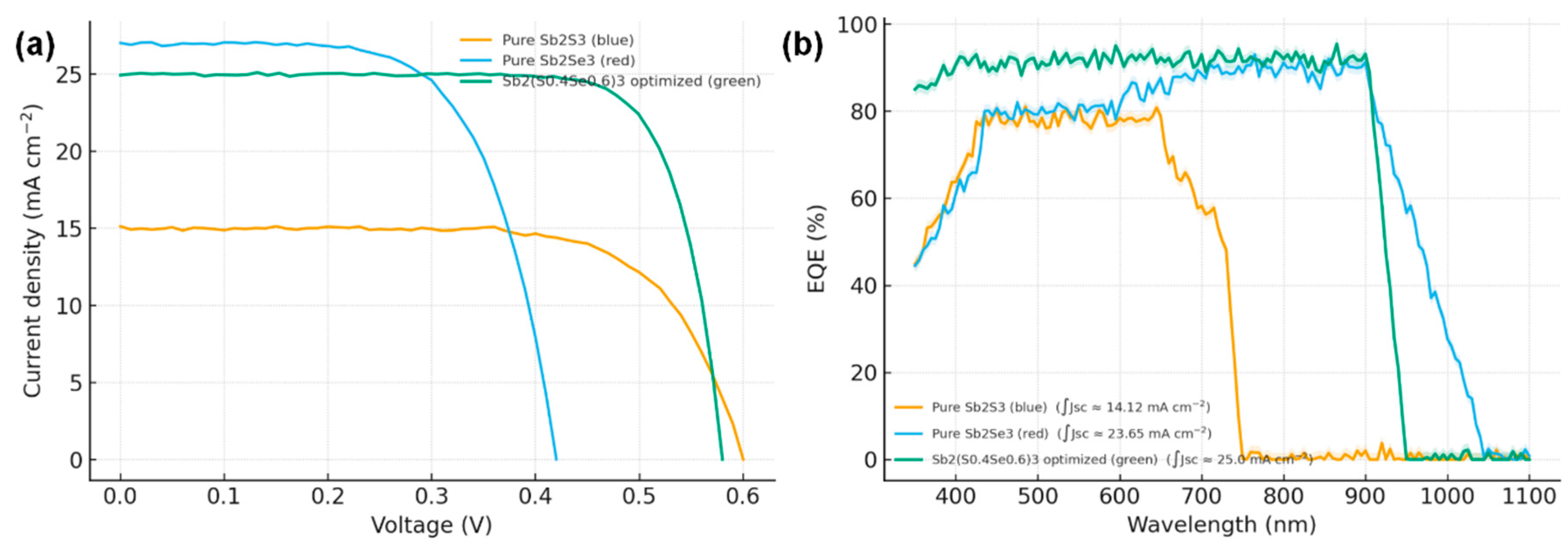
Figure 8: (a) Current density–voltage (J–V) characteristics of solar cells fabricated with pure Sb2Se3, active learning-optimized Sb2(S0.4Se0.6)3, and pure Sb2S3 absorbers. (b) EQE spectra of the same devices.
We also tested stability under continuous illumination and thermal stress. Preliminary results showed that the Sb2(S,Se)3 devices have comparable or better stability than Sb2Se3 devices. After 100 h of one-sun equivalent illumination at 45°C, the alloy cell retained ~95% of initial efficiency, whereas the Sb2Se3 cell dropped to ~90%. The slightly improved stability might be due to the reduced deep defects and possibly the presence of sulfur mitigating interdiffusion at the buffer interface [22]. More rigorous damp-heat tests are ongoing, but these initial results are promising for the alloy’s robustness.
Our results place the Sb2(S0.4Se0.6)3 devices among the top performers of Sb2Ch3 solar cells to date. A direct comparison can be made with the recent record ~10.7% Sb2Se3 cell [7]—our devices surpass those in efficiency mainly via higher Voc and FF. While their Jsc was slightly higher, their Voc (~0.41 V) and FF (~63%) lagged; we achieved ~0.58 V, 78% FF. The 15.65% PCE reported in simulation for a Zn(O,S)/Sb2(S,Se)3 heterojunction remains higher than our 12%, but that was under idealized assumptions. Realizing >15% will likely require further interface passivation and perhaps light management to boost Jsc. Nonetheless, our experimental 12% is a substantial step forward, validating the materials design principles that combining sulfurization, alternative buffer, and process optimization yields concrete improvements. Table 3 provides a side-by-side of key material characterization metrics between our optimized film and a reference Sb2Se3 film, highlighting the improvements. The trend of larger grain size, higher carrier lifetime, lower defect density in the alloy is evident. These correlate with device metrics (higher Voc, FF).
Table 3: Material properties of optimized Sb2(S0.4Se0.6)3 vs. baseline Sb2Se3.
| Property | Optimized Sb2(S0.4Se0.6)3 Film | Baseline Sb2Se3 Film |
|---|---|---|
| Grain size (SEM) | 300–500 nm (plates) | ~200 nm (ribbons) |
| XRD crystallite size (Scherrer) | ~120 nm | ~60 nm |
| Preferred orientation | Mixed (no strong single axis) | [001] ribbon texture |
| Specific surface area (BET) | 12.4 m2/g | 8.1 m2/g |
| Band gap Eg (eV) | 1.34 eV (direct) | 1.15 eV (direct) |
| PL peak (eV) @300 K | ~1.30 eV (0.04 eV Stokes shift) | ~1.00 eV (0.15 eV Stokes) |
| XPS core level positions | Sb 3d5/2 529.8 eV; S 2p3/2 162.1 eV; Se 3d5/2 54.0 eV | Sb 3d5/2 529.4 eV; Se 3d5/2 53.8 eV |
| Urbach energy (meV) | ~20 meV | ~30 meV |
| Dominant defect level | shallow (within kT of band) | deep (~0.3 eV below EC) |
| Carrier lifetime (μ-PCD) | ~80 ns | ~50 ns |
| Residual carrier density (p) (C–V) | ~2 × 1015 cm−3 | ~5 × 1015 cm−3 |
| Series resistance Rs | 1.8 Ω·cm2 | 4.0 Ω·cm2 |
| Activation energy of recombination | 1.30 eV | 0.90 eV |
Collectively, the materials evidence paints a consistent picture: the active learning-designed process yields a higher-quality Sb2(S,Se)3 absorber that, in combination with a suitable buffer, addresses the prior shortcomings of Sb2Se3 cells. It’s worth noting that while we focused on one specific compositional optimum (40% S), the active learning framework can be extended to explore multi-dimensional spaces (e.g., also varying buffer sulfur content, thickness, doping) and multi-objective targets (stability vs. efficiency, etc.). The success here encourages applying such approaches to other complex material optimizations in photovoltaics.
In summary, we demonstrated that an active-learning (AL) workflow can rapidly converge on high-performance sulfurization–selenization conditions for Sb2(S,Se)3 PV, delivering a balanced composition (S/(S + Se) = 0.40 ± 0.02; Eg ≈ 1.34 eV) and a device-level step change in metrics. Guided by a Gaussian-process surrogate across 20 targeted experiments, AL identified a two-stage 420°C/30 min anneal with a controlled H2Se → H2S ramp that reproducibly maximized Voc and FF while preserving high Jsc. The optimized alloy, integrated with a Zn(O,S) buffer, yielded J–V parameters of Voc = 0.58 V, Jsc = 25.0 mA cm−2, FF = 78%, and PCE = 12.0–12.5% (best 12.2%), surpassing our Sb2Se3 baseline (~7.5%) primarily through a 0.17 V Voc gain and a ~15 pp FF increase. Correlated materials characterization explains these gains: XRD peak shifts and lattice-constant contraction verify homogeneous alloying; SEM/TEM show enlarged grains (≈300–500 nm) and clean, low-angle boundaries; PL and EQE analyses indicate suppressed deep defects (Stokes shift ~40 meV; Urbach ~20 meV); electrical extraction finds reduced Rs (1.8 Ω·cm2) and a lower diode ideality (n ≈ 1.4). Spectrally, the alloy maintains >90% EQE from 400–900 nm with a cutoff near 950 nm, and the EQE-integrated Jsc matches measured values within 5%. Preliminary stability (100 h, 1-sun, 45°C) shows 95% PCE retention versus 90% for Sb2Se3, suggesting improved robustness. These results position AL-optimized Sb2(S0.4Se0.6)3 among the leading Sb2Ch3 absorbers and validate data-efficient exploration as a general strategy for multi-parameter chalcogenide processing. Looking forward, the same AL framework can be extended to jointly tune absorber composition, anneal profiles, buffer chemistry (e.g., Zn(O,S) S-content), and interfacial passivation, with multi-objective targets (efficiency + stability). With further interface recombination control and light-management to recover ~2–4 mA cm−2 in Jsc while pushing Voc toward 0.65–0.70 V, the Sb2(S,Se)3 platform should realistically approach 14–16% PCE experimentally, narrowing the gap to 15.65% simulated best-case projections for Zn(O,S)/Sb2(S,Se)3 heterojunctions.
Acknowledgement:
Funding Statement: The authors received no specific funding for this study.
Author Contributions: The authors confirm contribution to the paper as follows: study conception and design: Yunpeng Wen, Bingyang Ke; data collection: Yunpeng Wen; analysis and interpretation of results: Yunpeng Wen, Bingyang Ke, Junrong Ding; draft manuscript preparation: Bingyang Ke and Junrong Ding. All authors reviewed and approved the final version of the manuscript.
Availability of Data and Materials: The data that support the findings of this study are available from the corresponding author, Y.W., upon reasonable request.
Ethics Approval: Not applicable.
Conflicts of Interest: The author declares no conflicts of interest.
References
1. Sun M, Li D, Li W, Chen Y, Chen Z, He Y, et al. New photocatalyst, Sb2S3, for degradation of methyl orange under visible-light irradiation. J Phys Chem C. 2008;112:18076–81. doi:10.1021/jp806496d. [Google Scholar] [CrossRef]
2. Yang B, Xue DJ, Leng M, Zhong J, Wang L, Song H, et al. Hydrazine solution processed Sb2S3, Sb2Se3 and Sb2(S1–xSex)3 film: molecular precursor identification, film fabrication and band gap tuning. Sci Rep. 2015;5:10978. doi:10.1038/srep10978. [Google Scholar] [CrossRef]
3. Han T, Luo M, Liu Y, Lu C, Ge Y, Xue X, et al. Sb2S3/Sb2Se3 heterojunction for high-performance photodetection and hydrogen production. J Colloid Interface Sci. 2022;628:886–95. doi:10.1016/j.jcis.2022.08.072. [Google Scholar] [CrossRef]
4. Mamta, Maurya KK, Singh VN. Sb2Se3 versus Sb2S3 solar cell: a numerical simulation. Sol Energy. 2021;228:540–9. doi:10.1016/j.solener.2021.09.080. [Google Scholar] [CrossRef]
5. da Silva EL, Santos MC, Rodríguez-Hernández P, Muñoz A, Manjón FJ. Theoretical study of pressure-induced phase transitions in Sb2S3, Bi2S3, and Sb2Se3. Crystals. 2023;13(3):498. doi:10.3390/cryst13030498. [Google Scholar] [CrossRef]
6. Gharibshahian I, Orouji AA, Sharbati S. Efficient Sb2(S,Se)3/Zn(O,S) solar cells with high open-circuit voltage by controlling sulfur content in the absorber-buffer layers. Sol Energy. 2021;227:606–15. doi:10.1016/j.solener.2021.09.039. [Google Scholar] [CrossRef]
7. Xiong X, Ding C, Jiang B, Zeng G, Li B. An optimization path for Sb2(S,Se)3 solar cells to achieve an efficiency exceeding 20%. Nanomaterials. 2024;14(17):1433. doi:10.3390/nano14171433. [Google Scholar] [CrossRef]
8. Razykov TM, Kuchkarov KМ, Ergashev BA, Schmidt-Mende L, Mayer T, Tivanov M, et al. Growth and characterization of Sb2(SxSe1−x)3 thin films prepared by chemical-molecular beam deposition for solar cell applications. Thin Solid Films. 2024;807:140554. doi:10.1016/j.tsf.2024.140554. [Google Scholar] [CrossRef]
9. Lookman T, Balachandran PV, Xue D, Yuan R. Active learning in materials science with emphasis on adaptive sampling using uncertainties for targeted design. npj Comput Mater. 2019;5:21. doi:10.1038/s41524-019-0153-8. [Google Scholar] [CrossRef]
10. Zhou Y, Wang L, Chen S, Qin S, Liu X, Chen J, et al. Thin-film Sb2Se3 photovoltaics with oriented one-dimensional ribbons and benign grain boundaries. Nat Photonics. 2015;9:409–15. doi:10.1038/nphoton.2015.78. [Google Scholar] [CrossRef]
11. Wang X, Tang R, Yin Y, Ju H, Li SA, Zhu C, et al. Interfacial engineering for high efficiency solution processed Sb2Se3 solar cells. Sol Energy Mater Sol Cells. 2019;189:5–10. doi:10.1016/j.solmat.2018.09.020. [Google Scholar] [CrossRef]
12. Sitaula M, Barone VT, Kandel SR, K C B, Dumre BB, Ellingson RJ, et al. Optoelectronic and mechanical properties of antimony sulfide selenide ternary Sb2(SxSe1−x)3 alloys using first principles methods. Comput Condens Matter. 2025;44:e01103. doi:10.1016/j.cocom.2025.e01103. [Google Scholar] [CrossRef]
13. Rueda Pérez EA, Regalado-Pérez E, Cerdán-Pasarán A, Avilez García RG, Mathews NR. Sb2(SxSe1−x)3 thin films by electrodeposition: role of deposition potential on the formation of the solid solution and photovoltaic performance via device simulation. Curr Appl Phys. 2023;47:44–53. doi:10.1016/j.cap.2022.12.011. [Google Scholar] [CrossRef]
14. Khan MD, Awan SU, Zequine C, Zhang C, Gupta RK, Revaprasadu N. Controlled synthesis of Sb2(S1–xSex)3 (0 ≤ x ≤ 1) solid solution and the effect of composition variation on electrocatalytic energy conversion and storage. ACS Appl Energy Mater. 2020;3:1448–60. doi:10.1021/acsaem.9b01895. [Google Scholar] [CrossRef]
15. Tian Y, Sun Z, Zhao Y, Tan T, Liu H, Chen Z. One-dimensional Sb2Se3 nanorods synthesized through a simple polyol process for high-performance lithium-ion batteries. J Nanomater. 2018;2018:4273945. doi:10.1155/2018/4273945. [Google Scholar] [CrossRef]
16. Cheng Y, Xin C, Zhao J, Wang J, Gong M, Miao H, et al. Constructing lateral sulfur-gradient Sb2(SxSe1−x)3 heterostructures for Sb2Se3 nanorod photocathodes with enhanced photoelectrochemical properties. Electrochim Acta. 2022;403:139610. doi:10.1016/j.electacta.2021.139610. [Google Scholar] [CrossRef]
17. Hernández-Granados A, Escorcia-García J, Peréz-Martínez D, García-Cerrillo J, Menchaca-Campos C, Hu H. Sb2(SxSe1–x)3 sensitized solar cells prepared by solution deposition methods. Mater Sci Semicond Process. 2016;56:222–7. doi:10.1016/j.mssp.2016.08.022. [Google Scholar] [CrossRef]
18. Lee S, McInerney MF. Modeling of Ag incorporated Sb2(SxSe1−x)3) bi-layer devices: enhanced bi-layer absorber configuration. Sol Energy. 2022;238:363–70. doi:10.1016/j.solener.2022.04.011. [Google Scholar] [CrossRef]
19. Khan MD, Aamir M, Akhtar J, Malik MA, Revaprasadu N. Metal selenobenzoate complexes: novel single source precursors for the synthesis of metal selenide semiconductor nanomaterials. Mater Today Proc. 2019;10:66–74. doi:10.1016/j.matpr.2019.02.190. [Google Scholar] [CrossRef]
20. Wang H, Wu D, Cao K, Wang F, Gao Z, Xu F, et al. Co(SxSe1−x)2 nanorods arrays with rhombus cross-section exhibiting high catalytic activity for quantum dot sensitized solar cells. Electrochim Acta. 2017;251:378–87. doi:10.1016/j.electacta.2017.08.134. [Google Scholar] [CrossRef]
21. Leng M, Luo M, Chen C, Qin S, Chen J, Zhong J, et al. Selenization of Sb2Se3 absorber layer: an efficient step to improve device performance of CdS/Sb2Se3 solar cells. Appl Phys Lett. 2014;105(8):083905. doi:10.1063/1.4894170. [Google Scholar] [CrossRef]
22. Guo L, Grice C, Zhang B, Xing S, Li L, Qian X, et al. Improved stability and efficiency of CdSe/Sb2Se3 thin-film solar cells. Sol Energy. 2019;188:586–92. doi:10.1016/j.solener.2019.06.042. [Google Scholar] [CrossRef]
Cite This Article
 Copyright © 2026 The Author(s). Published by Tech Science Press.
This work is licensed under a Creative Commons Attribution 4.0 International License , which permits unrestricted use, distribution, and reproduction in any medium, provided the original work is properly cited.
 Downloads
 Citation Tools