
 Submit a Paper
 Propose a Special lssue
 Open Access
ARTICLE

FeS2 Film Properties and FeS2/Co-doped SnS2 Heterojunction for Photovoltaics Applications
1 Materials Physico-Chemistry Laboratory, Science and Technology Faculty, Chadli Bendjedid—El Tarf University, El Tarf, Algeria
2 Laboratory of Mechanical Engineering and Materials, Sciences Faculty, Physics Department, University 20 August 1955, Skikda, Algeria
3 Laboratory of study and research of condensed states (LEREC), Faculty of Sciences, University Badji Mokhtar, Annaba, Algeria
* Corresponding Authors: Kenza Kamli. Email: ,
Chalcogenide Letters 2026, 23(3), 7 https://doi.org/10.32604/cl.2026.076383
Received 19 November 2025; Accepted 09 February 2026; Issue published 03 April 2026
 View Full Text
 Download PDF
Abstract
We present a systematic investigation of FeS2 thin films deposited by ultrasonic spray pyrolysis (USP) at different deposition times (15–40 min), with the aim of understanding their structural, optical, and electrical evolution and their suitability for heterojunction device applications. Particular attention is given to the integration of the optimized FeS2 layer with a Co-doped SnS2 bottom layer to form a p–n heterojunction. Structural analysis by X-ray diffraction reveals a transition from an amorphous/oxidized phase at short deposition times toward well-crystallized pyrite after 25 min, while the 40-min film exhibits the most intense reflections and the largest crystallite size. Optical investigations indicate a progressive increase in film thickness from 0.23 to 1.53 μm between 20 and 40 min, accompanied by a reduction in the apparent optical band gap from 2.34 eV to 1.60 eV, consistent with improved crystallinity and enhanced light absorption. Electrical measurements further show a decrease in resistivity with increasing deposition time, together with improved carrier mobility and higher carrier concentration, confirming the enhancement of transport properties. The optimized FeS2 layer was subsequently coupled with a SnS2:Co film to fabricate a heterostructure, and current–voltage measurements reveal a pronounced rectifying response, confirming junction formation and charge separation at the interface. These findings demonstrate that deposition time plays a key role in tailoring FeS2 film properties and that the FeS2/SnS2:Co architecture constitutes a promising, low-cost heterojunction platform for future optoelectronic and photovoltaic device applications.Keywords
Supplementary Material
Supplementary Material FileCurrently, the researchers at different laboratories are investigating new materials for photovoltaic applications with a view to fabricating low-cost solar cell devices. There are a variety of semiconductor materials available now for solar cell fabrication, among these materials, the cubic system of FeS2 (pyrite) has attracted great attention as a potential candidate in photo-electrochemical and photovoltaic applications due to its diverse optical and physicochemical properties [1,2]. Their essential properties, pyrite major characteristics that make it suitable as an absorber material, for the application in thin-layers solar cells applications [1,3,4], and a higher optical absorption coefficient (α > 105 cm−1) in the near-infrared and in the visible range [5,6], FeS2 have a suitable optical energy gap (Eg = 0.95 eV) [7,8,9,10], which is in reality smaller than to the optimum value of 1.5 eV for solar cells [3,9], it is also known for its environmental compatibility as well as earth abundant, in addition it has low cost and nontoxic constituent elements [11,12]. Preceding studies attempted diverse techniques to elaborate pyrite thin films, which include: Chemical bath deposition method (CBD) [13], thermal sulfurization technique [14], and spray pyrolysis method [15]. Among these methods, the ultrasonic spray pyrolysis (USP) technique may be the most convenient technique because of its many advantages, such as: simplicity, low cost, easy to add doping materials and promising for high rate and mass production capability of uniform large area coatings in industrial applications [6,16]. In this paper, FeS2 samples have been elaborated by the ultrasonic spray pyrolysis method. The experimental conditions required to produce the samples FeS2 are described. The influence of the deposition time on the different properties (structural, optical and electrical) of pyrite (FeS2) thin films is also discussed.
2.1 Solutions and Thin Films Preparation
A homemade ultrasonic spray pyrolysis method (USP) was used to elaborate FeS2 thin films in this study, the details of this technique have been reported elsewhere [16]. The typical equipment of this technique consist a composed of an ultrasonic spraying system and a substrate holder with a heater. The ultrasonic vibrator frequency was 40 kHz. During the deposition, the nozzle-substrate distance was kept stable at 4 cm. These conditions were fixed, in our laboratory previously, to deposit successful such films by this technique. Before the deposition of FeS2 thin layers, the glass substrates were well cleaned firstly. FeS2 thin films were synthesized using an aqueous solution containing the following precursors: thiourea (SC (NH2)2) 6 × 10⁻² M and (FeCl3·6H2O) 3 × 10⁻² M as sulfur and iron sources, respectively. Different deposition times (which are: 15, 20, 25, 30, 35 and 40 min), were used. The substrate temperature, was fixed at 350°C, because it was found to be the optimum temperature value to obtain uniform and well-adherent FeS2 thin layers [6,15].
2.2 Characterisation Techniques
The crystalline quality of the prepared samples was examined by X-ray diffraction (XRD), using the copper radiation CuKα = 1.5418 Å in the 2θ range 15–75° with a step size of 0.013° and a scan time of 2 s per step. The optical transmission and reflectance spectra were performed using a UV-Vis-NIR spectrometer (Perkin Elmer lambda 950) at room temperature in the wavelength range between 300 and 800 nm with a step size of 5 nm. In addition, the electrical characteristics were measured using the ECOPIA Hall Effect Measurement system (HMS-3000) in van der Pauw configuration.
Fig. 1 shows the XRD spectra of FeS2 thin films formed onto preheated glass substrates at 350°C substrate temperature with different deposition times.
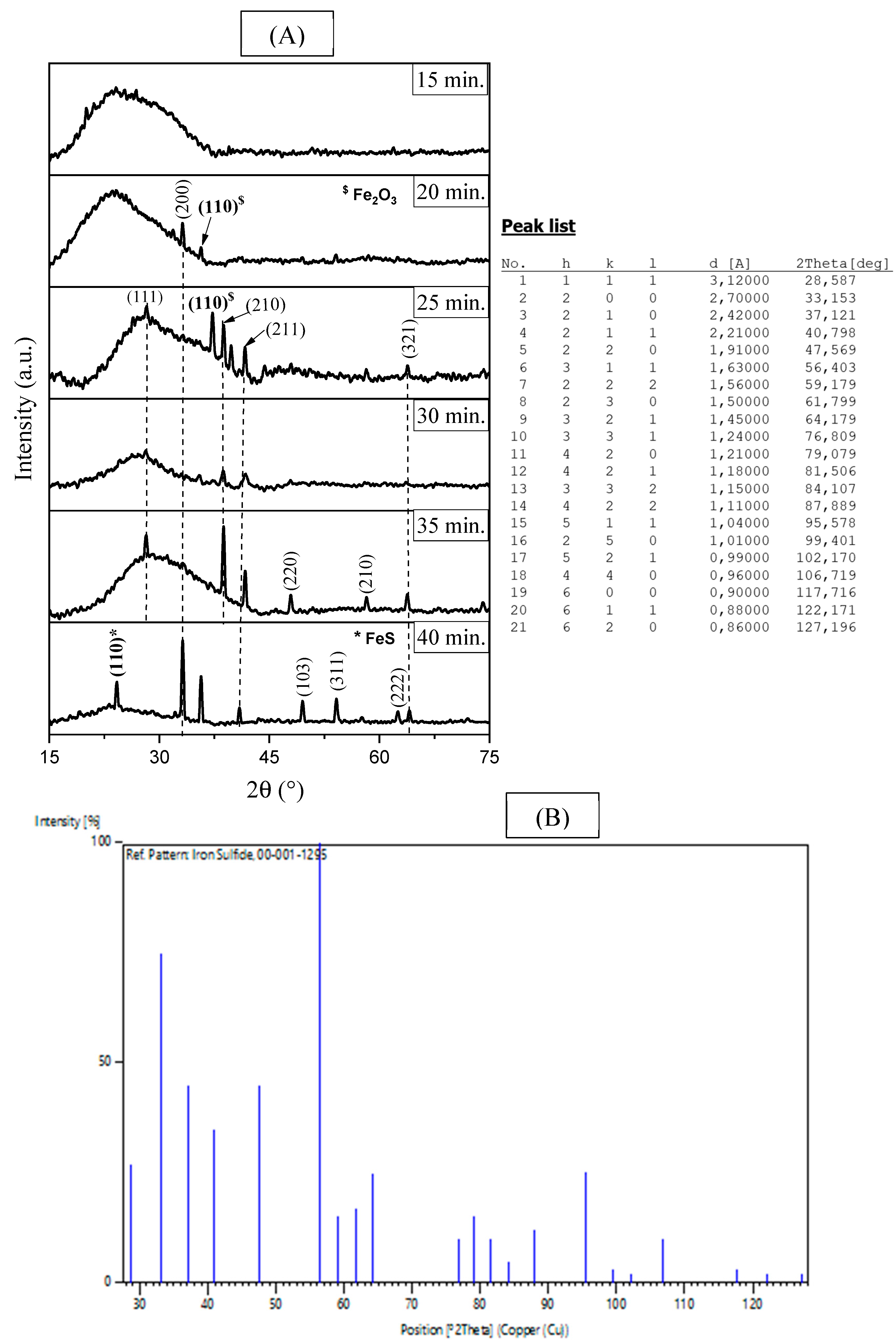
Figure 1: (A) XRD pattern of FeS2 thin films obtained at different deposition times, (B) PDF card no. 001-1295.
According to the Fig. 1A, it can be noticed that the films elaborated at short deposition times (15–20 min), represents an amorphous phase and intermediate oxides. The film obtained at 15 min shows only a broad “hump” situated in the small diffraction angles (<30°), characteristic of an amorphous or nanocrystalline layer whose thickness is insufficient to produce distinct Bragg peaks. However, for 20 min a weak peak emerges at 2θ ≈ 33° assigned to (200) plane of FeS2 cubic structure (according to PDF card no. 001-1295), alongside a feature marked Fe2O3 (PDF Card no. 01-073-0603), indicating partial oxidation of the iron precursor prior to full Fe–S formation [17]. Furthermore, Fe2O3 was found to accompany the preparation of FeS2 [15]. For the film obtained at 25 min, well-defined reflections indexed to cubic pyrite FeS2, namely (111), (210), (211) and (321) appear at the expected positions (JCPDS no. 001-1295 (Fig. 1B)). Besides, the disappearance of oxide peaks shows that sulfurization now dominates over oxidation. With increasing the deposition times to 30 min, FeS2 peak intensities decrease slightly and broaden. This may arise from increased internal strain or a high density of grain boundaries, a phenomenon frequently observed in spray-pyrolysis when growth is too rapid [5].
After 35 min of deposition, a new peak (110) indexed to monosulfide FeS (JCPDS no. 01-080-1029) appears. This means that FeS2 has partially broken down or that sulphur has been depleted in the area where the spray has been going on for a long time [5]. At 40 min, a weak additional reflection indexed to FeS (110) becomes visible, indicating that a minor sulfur-deficient phase persists at long deposition times. Its relative contribution has been estimated, by introducing a semi-quantitative ratio:
The evolution of crystallite size D, microstrain ε, and dislocation density δ in FeS2 films as a function of deposition time are given in Fig. 2. The most intense and well-resolved peak in the diffraction patterns for each sample was used for crystallite size, microstrain, and dislocation density calculations. These parameters can be understood in terms of classical XRD line-broadening analysis (Scherrer formula) and defect-density scaling.
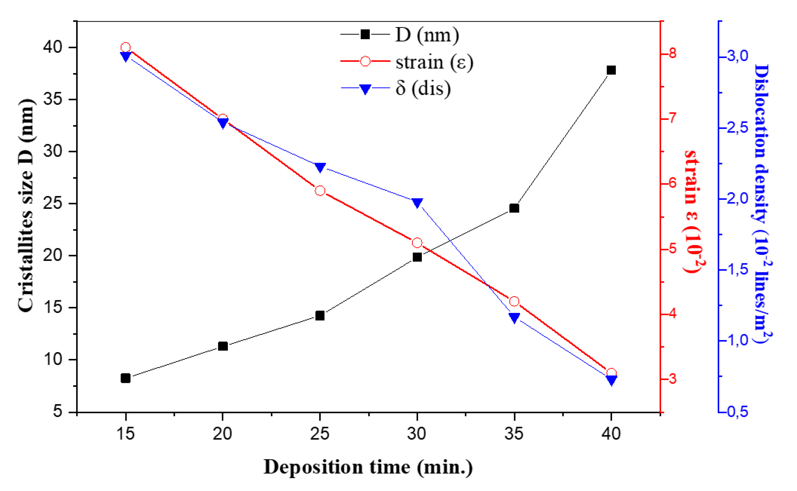
Figure 2: Variation of grain size, strains and dislocation density of FeS2 versus the deposition time.
The crystallite size (D) is estimated by using the well-known Scherrer’s formula [18].
According to the Fig. 2, it can be noticed that D rises monotonically from ≈ 8 nm at 15 min to ≈ 38 nm at 40 min. Longer ultrasonic-spray durations deposit more material and allow grain–boundary migration under 350°C heat, promoting coalescence of nanocrystallites into larger coherent domains. This trend is habitually observed in spray-pyrolysis [19] and other vapor–deposition techniques.
Despite the enlargement of the crystallite size with deposition time elevation, their values remain in the nano-crystalline order and these small sizes of the grains have many advantages such as: the increase of exchange surfaces and reactivity.
Using the grain size values, the strain ε is assessed using the following relation [18]:
From the other side, the lattice strain extracted via Eq. (2), drops from ~0.08 at 15 min to ~0.03 at 40 min which is in good correlation with crystallite size variation. Small crystallites accommodate a high density of lattice defects (dislocations, surface stress), yielding larger peak broadening from microstrain. As grains grow, many of these defects annihilate at grain boundaries or reorganize into lower-energy configurations, so the average internal strain falls [17,20].
The dislocation density δ(dis) developed of FeS2 thin films were evaluated by using the Eq. (3) [18].
The calculated δ(dis) decreases from ≈3.0 × 10⁻² nm−2 at 15 min down to ≈6.9 × 10⁻⁴ nm−2 at 40 min. This inverse-square relation is a standard approximation linking coherent-domain size to average dislocation density in polycrystalline films. Physically, as grains enlarge, the number of dislocations per unit volume drops dramatically because many dislocations either exit the grain or form low-energy networks at boundaries [16].
3.2.1 Transmittance, Absorbance and Reflectance Properties
The optical transmission T(λ) of iron disulfide (FeS2) thin films deposited on glass substrates via ultrasonic spray pyrolysis at a substrate temperature of 350°C are shown in Fig. 3.
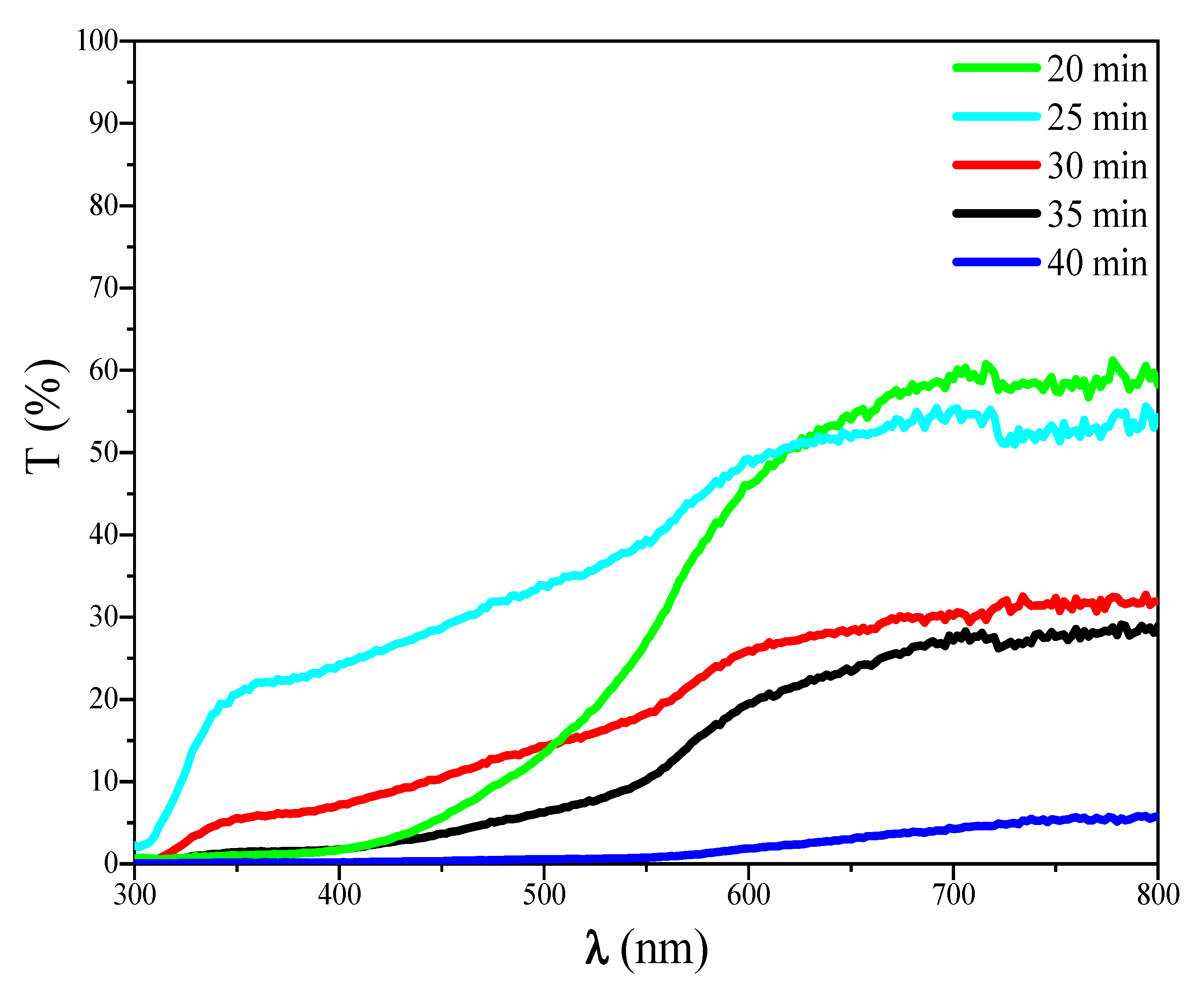
Figure 3: Transmission spectra of FeS2 thin films with different deposition times.
It is well known that, in general films’ transmittance increases with the reduction of film thickness [19], which is the case of transmittance variation in FeS2 layers. From Fig. 3, it is notable that the transmittance starts high at a shorter deposition time than decreases gradually with deposition time elevation, reaching almost 5% for 40 min, with oscillatory fringes. These fringes arise from interference effects in thin films, indicating uniform thickness and good surface quality.
Moreover, the inverse relationship between the transmittance and time is due to thicker films from prolonged deposition, which scatter and absorb more light. Comparable trends are observed in spray-pyrolyzed FeS2 films, where increased thickness (correlated with deposition parameters like time or temperature) reduces transmittance in the visible region [21].
The absorbance was calculated from the measured transmission using:
Around 725 nm, the 40 min film exhibits very low transmission (~4.8%), corresponding to a high absorbance (A ≈ 1.32) and a large absorption coefficient of approximately 1.3 × 105 cm−1.
In contrast, the other samples show significantly higher transmission and much lower α values (~103–104 cm−1). Consequently, the condition αt ≫ 1, which leads to a square-like suppression of transmission, is fulfilled only for specific samples and spectral regions. This explains why the pronounced transmission drop is observed only in certain films and highlights the combined role of absorption strength and film thickness in governing the optical response. The calculated absorption coefficient values at representative wavelengths are summarized in Table 1.
Table 1: Absorption coefficient α(λ) of FeS2 thin films at selected wavelengths derived from measured transmission and thickness.
| Deposition Time | α (cm−1) |
|---|---|
| 40 min | ≈1.3 × 10⁵ |
| 35 min | ≈2.4 × 10⁴ |
| 30 min | ≈9.8 × 10³ |
| 25 min | ≈5.4 × 10³ |
| 20 min | ≈3.6 × 10³ |
As the deposition time increases from 20 to 40 min, a clear enhancement of optical absorption is observed, particularly in the long-wavelength region (500–800 nm). Pyrite FeS2 is known to exhibit very high absorption coefficients in the visible range, with reported values on the order of 104–105 cm−1 [22]. Such high absorption implies that even relatively thin films can absorb a large fraction of incident visible light, while thicker films obtained at longer deposition times become effectively non-transmitting. This behavior explains why the 40 min film shows the highest absorption response, whereas the 20-min film exhibits the lowest. In addition, the increase in deposition time leads to thicker films, which further enhances absorption through an increased optical path length [23].
3.2.2 Thickness and Band Gap Measurement
Using the optical data, the envelope method is employed in order to calculate FeS2 thin films thickness (t) from two minima or maxima using the expression (6) [24].
The optical band gaps (Eg) of FeS2 thin films has been determined on the basis of UV-VIS-NIR spectrophotometer by plotting (αhν)2 as a function of hν, which are linear over a wide range of photon energies indicating the direct type of transitions.
The optical band gap is obtained from the plot of the following relation [9]: (αhν)2 = A (hν − Eg)(7) where α is the absorption coefficient, A is a constant, Eg is the optical band gap, ν is the frequency of the incident photon and h is the Planck’s constant. The band gap energies of these films are determined from the intercept of the tangent to the plot with the abscissa axis as indicated in Fig. 4.
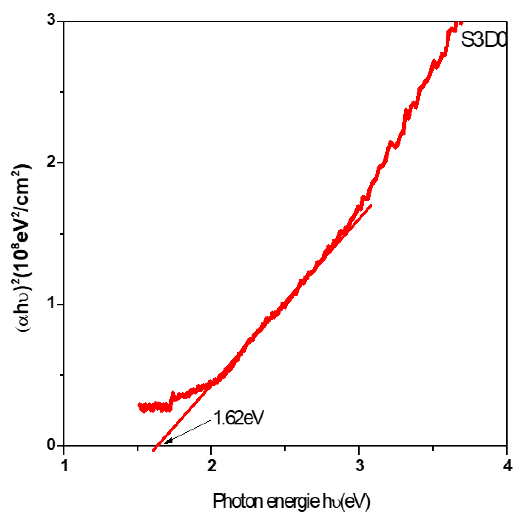
Figure 4: Plot of (αhν)2 versus photon energy (hν) of FeS2 thin films obtained at 35 min.
The obtained thickness and optical band gap values of FeS2 films deposited at different durations are summarized in Table 2. These values are in agreement with the reported values in the literature [6].
Table 2: Films thickness (t) and band gap (Eg) for different deposition time.
| Deposition Time (min) | t (μm) | Eg (eV) |
|---|---|---|
| 20 | 0.23 | 2.34 |
| 25 | 0.56 | 1.81 |
| 30 | 1.17 | 1.73 |
| 35 | 1.25 | 1.62 |
| 40 | 1.53 | 1.60 |
Table 2 illustrates the dependence of film thickness (t) and optical band gap (Eg) on deposition time for FeS2 thin films prepared by ultrasonic spray pyrolysis at 350°C on glass substrates. The film thickness increases with deposition time, starting at 0.23 μm for 20 min and rising to 1.53 μm for 40 min, this increase is approximately linear. This correlation between longer time deposition and film thickness elevation is a standard outcome in time-controlled deposition techniques, where thickness scales with exposure duration until saturation or peeling effects occur. In spray pyrolysis [16,19], longer deposition times allow for greater accumulation of atomized precursor material (Fe and S sources) on the heated substrate, leading to thicker films.
Besides, the band gap decreases monotonically with increasing deposition time, from 2.34 eV at 20 min to 1.60 eV at 40 min. The high optical gap (2.34 eV) at 20 min is mainly due to iron oxide (Fe2O3) and amorphous intermediate phases, as shown by XRD. These phases exhibit wider band gaps than pyrite FeS2, directly linking the structural and optical observations, in agreement with reported Fe–S–O thin-film studies [24]. As the deposition time rises (thickness rises) the films become more continuous, better sulfurized and more dominated by the pyrite phase as it have been noticed from the DRX and optical results, these characteristics make the optical gap moves toward the intrinsic pyrite value (which is lower). Several spray-deposition studies [25,26] of Fe–S films report high apparent Eg (>1.5–2.0 eV) for short/poorly sulfided films and lower Eg for thicker, better-crystallized pyrite films.
These obtained results confirms that due to absorption coefficients exceeding 104–105 cm−1, FeS2 requires only tens to a few hundreds of nanometers to absorb most incident visible light. This point is emphasized to reinforce FeS2’s suitability as an ultra-thin absorber layer for photovoltaic devices, consistent with established literature [27].
The electrical properties of the FeS2 thin films are determined at room temperature by Hall Effect measurements system. The obtained results for the best-deposited FeS2 thin films are summarized in Table 3.
Table 3: Resistivity (ρ), volume carrier concentration (Nv), surface carrier concentration (Ns), Hall mobility (μ) and conductivity type of the deposited FeS2 thin films.
| Deposition Time (min) | ρ (Ω. cm) × 104 | Nv (cm−3) × 1012 | Ns (cm−2) × 107 | μ (cm2/Vs) × 101 | Type |
|---|---|---|---|---|---|
| 30 | 9.561 | 0.049 | 0.576 | 0.080 | P |
| 35 | 6.048 | 5.514 | 9.025 | 4.689 | P |
| 40 | 0.241 | 12.890 | 12.680 | 13.260 | P |
As shown in the Table 3, as per deposition time increases, resistivity decreases while carrier concentrations, surface carrier concentration and mobility increase but the conductivity type remains always P-type conduction. The resistivity ρ falls from 30 to 40 min. This is expected when films become thicker, more continuous and contain more percolating conducting pathways. Increased thickness and densification reduce sheet/grain-boundary resistance, producing higher macroscopic conductivity [19,20]. Spray-pyrolysis and thin-film studies commonly report resistivity decreasing with film thickness and grain growth. On the other hand, Nv rises from 4.9 × 10¹⁰ to 1.29 × 1013 cm−3. This can reflect (i) approaching the correct FeS2 stoichiometry (reduction of insulating oxides), (ii) creation of donor/acceptor defects with film growth (e.g., S vacancies or Fe interstitials), or (iii) the emergence of a different, more conductive phase (FeS/pyrrhotite) that contributes higher free carrier density (as it have been noticed from the DRX results). Pyrite often shows widely varying n depending on stoichiometry and impurities [22,28].
Besides, Hall mobility (μ) reported increases from 0.8 to 132.6 cm2/(V·s). This behavior of larger μ at longer deposition times is consistent with grain growth and reduced defect scattering, because larger grains reduce grain-boundary scattering and traps, and better crystallinity lowers ionized-impurity and defect scattering, both raising mobility. Reported mobility values for pyrite single crystals can reach 102–103 cm2/(V·s) in the literature.
3.4 Current-Voltage Characteristics of FeS2/SnS2:Co Heterojunction
After studying the structural, optical, and electrical properties of iron sulphide film, FeS2 thin film was deposited on 4% Co doped tin sulfide film obtained at 400°C glass substrate temperature [29], and the properties of a current-voltage diagram were drawn to figure out I–V characteristics in the forward and reverse biases, Fig. 5 shows the behaviour of FeS2/SnS2:Co heterojunction. The complete set of electronic and optical parameters used for the SCAPS-1D simulation of the FeS2/SnS2:Co heterostructure is provided in Table S1 (Supplementary Material) for reproducibility.
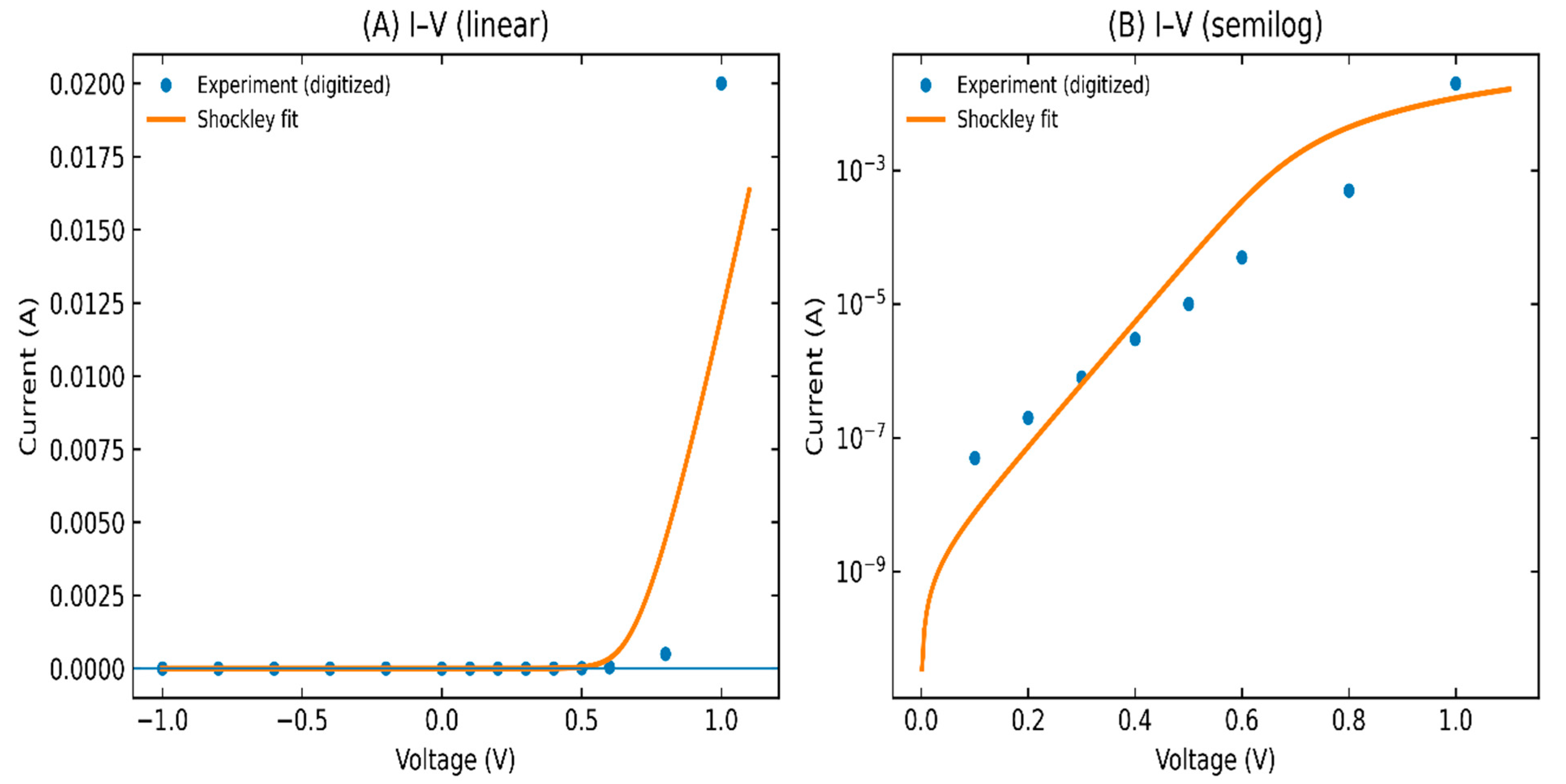
Figure 5: I–V variation (A) linear variation and (B) semilog variation of FeS2/SnS2:Co structure.
The dark current–voltage characteristics of the FeS2/SnS2:Co heterojunction were fitted with the Shockley diode model including series and shunt resistances. The implicit nonlinear regression produced a saturation current I0 = (1.00 ± 0.01) × 10−9 A, an ideality factor n = 1.80 ± 0.01, a series resistance Rs = 20.0 ± 0.1 Ω, and an effectively infinite shunt resistance (Rsh ≫ 1011 Ω; the fit returned a large-magnitude negative value due to parameter covariance, indicating vanishing leakage). An ideality factor close to two suggests recombination-assisted transport in the space-charge region, as opposed to solely diffusion-limited thermionic emission. The moderate Rs aligns with the anticipated contributions from contact and grain boundaries in spray-deposited chalcogenide thin films. The very high Rsh shows that the junction is very well isolated and that there is almost no parallel leakage [30,31,32]. These results show that FeS2 deposited on Co-doped SnS2 films can create a working p–n heterojunction that can be used in optoelectronic devices.
The current study demonstrates that ultrasonic spray-deposited FeS2 films transition from poorly crystallized/oxidic layers at brief deposition durations to well-crystallized pyrite at extended durations (40 min), accompanied by an increase in coherent domain size (from 8 to 38 nm) and a significant decrease in microstrain and dislocation density. As the deposition time increases, the films become thicker (about 0.23 to 1.53 μm) and much more absorbing. The apparent optical gap shifts from about 2.34 eV to about 1.60 eV, but the absorption coefficient in the visible range stays very high. This means that only tens to hundreds of nanometres of active FeS2 are needed to absorb most of the sunlight that hits it. The films are p-type electrically, and their resistivity goes down over time because the carrier concentration goes up and the mobility improves (grain growth and less defect scattering). Combining the optimised FeS2 (40 min) with Co-doped SnS2 made a strong rectifying heterojunction: implicit Shockley fits yield I0 ≈ 1.01 × 10⁻⁹ A, ideality factor n ≈ 1.80, Rs ≈ 20 Ω and an effectively negligible shunt leakage (Rsh); the device has strong rectification (the measured rectification ratio is >104 at ±1 V).
These optical and electrical properties make the FeS2/SnS2:Co heterostructure a great choice for cheap solar cells: FeS2 is a strong absorber that is found in large amounts on Earth. This means that the active layer can be kept thin. The Co-doped SnS2 bottom layer, on the other hand, is a compatible, conductive n-type partner that forms the p–n junction.
The detailed electronic and optical parameters adopted for FeS2 absorber modeling, along with their scientific basis and literature justification, are provided in Table S2 (Supplementary Material).
Acknowledgement:
Funding Statement: The authors received no specific funding for this study.
Author Contributions: All authors contributed to the conception, design, analysis, and interpretation of the results. Kenza Kamli and Naoual Houaidji contributed to the conceptualization of the study and development of the methodology. Zakaria Hadef carried out the experimental investigation and data acquisition, while Houssem Eddine Chouial and Marwa Bendaia performed the software-related work and formal analysis. Data curation and preparation of the original draft were conducted by Kenza Kamli. The manuscript was reviewed and edited by Naoual Houaidji and Kenza Kamli. Visualization of the results was prepared by Zakaria Hadef. Supervision and project administration were ensured by Kenza Kamli. All authors reviewed and approved the final version of the manuscript.
Availability of Data and Materials: The data that support the findings of this study are available from the corresponding author, Kenza Kamli, upon reasonable request. All raw and processed data related to structural (XRD), optical (UV–Vis–NIR), and electrical (Hall effect, I–V) measurements are securely stored, and can be shared for academic and research purposes.
Ethics Approval: The authors agree with Compliance with Ethical Standards of Chalcogenide Letters. The authors declare that this article is conforming to ethical standards and does not contain any studies with human or animal subjects.
Conflicts of Interest: The authors declare no conflicts of interest.
Supplementary Materials: The supplementary material is available online at https://www.techscience.com/doi/10.32604/cl.2026.076383/s1. Table S1: Electronic and optical parameters of FeS2 absorber and SnS2:Co buffer layers used as input for SCAPS-1D heterojunction simulation. Table S2: Electronic and optical parameters adopted for the FeS2 absorber layer in SCAPS-1D simulations, with corresponding scientific justification and literature basis.
References
1. Singh K , Kaur M , Sharma RK , Sharma N , Kumar A . Structural, morphological and charge transport properties of FeS2 nanostructures. Trans Electr Electron Mater. 2025; 26: 232. doi:10.1007/s42341-025-00590-3. [Google Scholar] [CrossRef]
2. Sun J , Song S , Xia Q , Huang Z , Wang S , Zhang L , et al. Constructing CoS2/FeS2 heterostructures on hollow carbon spheres with promoted reaction kinetics for high-rate and stable sodium storage. J Energy Storage. 2025; 107: 115013. doi:10.1016/j.est.2024.115013. [Google Scholar] [CrossRef]
3. Singh J , Singh K , Kaur M , Sharma RK , Vij A , Kumar A . MoS2/FeS2 nanocomposite thin film: Structural, morphological, compositional, electrical and photodetection properties. Chem Phys Lett. 2021; 783: 139047. doi:10.1016/j.cplett.2021.139047. [Google Scholar] [CrossRef]
4. Reedo K , Raadik T , Altosaar M , Pilvet M , Gutjuma A , Krustok J , et al. Scalable phosphorus doping of p-type FeS2 Microcrystals for photovoltaic applications. ACS Omega. 2025; 10( 48): 58869– 76. doi:10.1021/acsomega.5c07455. [Google Scholar] [CrossRef]
5. Al Khateeb S , Sparks TD . Pore-graded and conductor- and binder-free FeS2 films deposited by spray pyrolysis for high-performance lithium-ion batteries. J Mater Res. 2019; 34: 2456. doi:10.1557/jmr.2019.208. [Google Scholar] [CrossRef]
6. Fatehi MW , Ali HS , Ismail RA , Salih EY . Nanostructured n-FeS2/SiO2/p-Si heterojunction for self-driven Vis-NIR photodetection. Micro Nanostruct. 2025; 208: 208383. doi:10.1016/j.micrna.2025.208383 [Google Scholar] [CrossRef]
7. Cedeño Morales E , Peña Méndez Y , Gamboa-Sánchez SA , Ildusovich Kharissov B , Hernández García TC , Garza-Navarro MA . Tunable bandgap in cobalt-doped FeS2 thin films for enhanced solar cell performance. Materials. 2025; 18( 19): 4546. doi:10.3390/ma18194546. [Google Scholar] [CrossRef]
8. Zaka A , Alhassan S , Nayfeh A . Understanding the phase changes and optical properties in the solvothermal synthesis of iron pyrite. Sci Rep. 2025; 15: 18763. doi:10.1038/s41598-025-03692-3. [Google Scholar] [CrossRef]
9. Chakraborty RN , Mahanta DS , Senthilkumar K . Investigation of FeS2 thin film as a hole transport layer in CuAl1−xFexS2-based solar cells: a strategy to improve efficiency. ACS Appl Energy Mater. 2025; 8: 4272. doi:10.1021/acsaem.4c03187. [Google Scholar] [CrossRef]
10. Ouertani B , Ezzaouia H , Theys B . Effect of ruthenium alloy on the band gap value of FeS2-pyrite. Colloids Surf A Physicochem Eng Aspects. 2017; 525: 13– 9. doi:10.1016/j.colsurfa.2017.04.038. [Google Scholar] [CrossRef]
11. Kment S , Kmentova H , Sarkar A , Soukup RJ , Ianno NJ , Sekora D , et al. Epoxy catalyzed sol–gel method for pinhole-free pyrite FeS2 thin films. J Alloys Compd. 2014; 607: 169– 76. doi:10.1016/j.jallcom.2014.04.060. [Google Scholar] [CrossRef]
12. Vedavathi A , Reddy YM , Reddy KR . Effect of precursor concentration on structural and morphological properties of iron pyrite thin films. Procedia Mater Sci. 2015; 10: 279– 84. doi:10.1016/j.mspro.2015.06.051. [Google Scholar] [CrossRef]
13. Yu Q , Cai S , Jin Z , Yan Z . Evolutions of composition, microstructure and optical properties of Mn-doped pyrite (FeS2) films prepared by chemical bath deposition. Mater Res Bull. 2013; 48: 3601. doi:10.1016/j.materresbull.2013.05.074. [Google Scholar] [CrossRef]
14. Liu X , Jacob Y , Ho L , Wong M , Kwok HS , Liu Z . Synthesis, characterization and fabrication of ultrathin iron pyrite (FeS2) thin films and field-effect transistors. RSC Adv. 2016; 6: 8290. doi:10.1039/C5RA23344E. [Google Scholar] [CrossRef]
15. Ouertani B , Ouerfelli J , Saadoun M , Bessais B , Hajji M , Kanzari M , et al. Transformation of amorphous iron oxide films pre-deposited by spray pyrolysis into FeS2-pyrite films. Mater Lett. 2005; 59: 734– 9. doi:10.1016/j.matlet.2004.06.074. [Google Scholar] [CrossRef]
16. Kamli K , Hadef Z , Kamli O , Chouial B , Aida MS , Hadjoudja H , et al. Effect of deposition time on the properties of CuxZnyS thin films synthesized by ultrasonic spray pyrolysis. J Nano Res. 2023; 81: 37. doi:10.4028/p-DPoy5X. [Google Scholar] [CrossRef]
17. Mustafa MI , Mustafa AH , Khaleel IH . Characterization of FeS2 thin film prepared by spray pyrolysis method for optoelectronic applications. J Appl Sci Nanotechnol. 2022; 2: 78– 84. doi:10.53293/jasn.2022.3961.1115. [Google Scholar] [CrossRef]
18. Hadef Z , Kamli K , Akkari A , Hadjoudja H , Kamoun NT , Kamli O , et al. In-depth characterization of physical proprieties of SnS: Mg thin films fabricated by ultrasonic spray for solar cell applications. J Mater Sci Mater Electron. 2024; 35( 24): 1632. doi:10.1007/s10854-024-13370-1. [Google Scholar] [CrossRef]
19. Mekhbi O , Kamli K , Hadef Z , Kamli O , Bouatrous M , Houaidji N , et al. Enhanced performance of tin sulfide thin-film solar cells via silicon substrate integration: a combined experimental and simulation study. Chalcogenide Lett. 2025; 22: 331. doi:10.15251/CL.2025.224.331. [Google Scholar] [CrossRef]
20. Kamli K , Hadef Z , Kamli O , Kamoun NT , Messaoudi M . Fabrication of high-quality graphene-doped copper zinc sulfide (CZS:Gr) absorbers thin films. J Mater Sci Mater Electron. 2025; 36( 19): 1155. doi:10.1007/s10854-025-15252-6. [Google Scholar] [CrossRef]
21. Daranfed W , Aida MS , Hafdallah A , Lekiket H . Substrate temperature influence on ZnS thin films prepared by ultrasonic spray. Thin Solid Film. 2009; 518: 1082. doi:10.1016/j.tsf.2009.03.227. [Google Scholar] [CrossRef]
22. Srivastava RP , Ingole S . An investigation on the phase purity of iron pyrite (FeS2) thin films obtained from the sulfurization of hematite (Fe2O3) thin films. Mater Sci Semicond Process. 2020; 106: 104775. doi:10.1016/j.mssp.2019.104775. [Google Scholar] [CrossRef]
23. Banjara D , Malozovsky Y , Franklin L , Bagayoko D . First-principles studies of electronic, transport and bulk properties of pyrite FeS2. AIP Adv. 2018; 8( 2): 025212. doi:10.1063/1.4996551. [Google Scholar] [CrossRef]
24. Akkari A , Guasch C , Castagne M , Kamoun-Turki N . Optical study of zinc blend SnS and cubic In2S3:Al thin films prepared by chemical bath deposition. J Mater Sci. 2011; 46: 6285. doi:10.1007/s10853-011-5626-1. [Google Scholar] [CrossRef]
25. Kmentova H , Kment S , Hubicka Z , Remes Z , Olejnicek J , Cada M , et al. Thermal sulfidation of α-Fe2O3 hematite to FeS2 pyrite thin electrodes: correlation between surface morphology and photoelectrochemical functionality. Catal Today. 2018; 313: 224. doi:10.1016/j.cattod.2017.11.004. [Google Scholar] [CrossRef]
26. Ouertani B , Ouerfelli J , Saadoun M , Bessais B , Ezzaouia H , Bernéde JC . Characterization of FeS2-pyrite thin films synthesized by sulphuration of amorphous iron oxide films pre-deposited by spray pyrolysis. Mater Charact. 2005; 54: 431. doi:10.1016/j.matchar.2005.01.009. [Google Scholar] [CrossRef]
27. Prabukanthan P , Lakshimi R , Rajesh Kumar T , Thamaraiselvi S , Harichandran G . Electrochemical deposition of p-type FeS2 thin films absorber layer for photovoltaic cell. Adv Mater Proc. 2017; 2: 521. doi:10.5185/amp.2017/811. [Google Scholar] [CrossRef]
28. Schieck R , Hartmann A , Fiechter S , Könenkamp R , Wetzel H . Electrical properties of natural and synthetic pyrite (FeS2) crystals. J Mater Res. 1990; 5( 7): 1567– 72. doi:10.1557/jmr.1990.1567. [Google Scholar] [CrossRef]
29. Zhang X , Scott T , Socha T , Nielsen D , Manno M , Johnson M , et al. Phase stability and stoichiometry in thin film iron pyrite: impact on electronic transport properties. ACS Appl Mater Interfaces. 2015; 7( 25): 14130– 9. doi:10.1021/acsami.5b03422. [Google Scholar] [CrossRef]
30. Hadef Z , Kamli K , Kamli O , Labiod S . Effect of substrate temperature on physical properties of Co doped SnS2 thin films deposited by ultrasonic spray pyrolysis. Chalcogenide Lett. 2023; 20( 8): 587– 97. doi:10.15251/cl.2023.208.587. [Google Scholar] [CrossRef]
31. Sze SM , Ng KK . Physics of semiconductor devices. Hoboken, NJ, USA: John Wiley & Sons, Inc.; 2006. doi:10.1002/0470068329. [Google Scholar] [CrossRef]
32. Schroder DK . Semiconductor material and device characterization. Hoboken, NJ, USA: John Wiley & Sons, Inc.; 2005. doi:10.1002/0471749095. [Google Scholar] [CrossRef]
Cite This Article
 Copyright © 2026 The Author(s). Published by Tech Science Press.
This work is licensed under a Creative Commons Attribution 4.0 International License , which permits unrestricted use, distribution, and reproduction in any medium, provided the original work is properly cited.
 Downloads
 Citation Tools