
 Submit a Paper
 Propose a Special lssue
 Open Access
ARTICLE

Effect of Annealing on CuZnS Ternary Chalcogenide Thin Films Prepared by Chemical Bath Deposition: An XPS Study
1 Post Graduate Department of Physics, Sree Narayana College, University of Calicut, Nattika, Kerala, India
2 PG and Research Department of Physics, Sree Kerala Varma College, University of Calicut, Thrissur, Kerala, India
* Corresponding Author: Preetha K. C.. Email:
Chalcogenide Letters 2026, 23(3), 6 https://doi.org/10.32604/cl.2026.076854
Received 27 November 2025; Accepted 02 March 2026; Issue published 03 April 2026
 View Full Text
 Download PDF
Abstract
The increasing depletion of fossil fuels and the escalation of global temperatures have intensified the need for sustainable energy sources such as solar power. Copper Zinc Sulphide (CuZnS) is a potential absorber for solar cells. This study reports the structure and composition of annealed CuZnS samples using X-ray Photoelectron Spectroscopy (XPS) analysis technique. CuZnS thin films prepared using low-cost chemical bath deposition (CBD) technique are annealed at 100°C, 200°C, and 300°C. The samples are analysed using Energy Dispersive X-ray Spectroscopy (EDX), X-ray Diffraction (XRD), Scanning Electron Microscopy (SEM), UV Visible NIR spectroscopy (UV-VIS) and Hall effect measurements. XPS and EDX analyses confirmed an increase in zinc content with annealing, accompanied by a decrease in sulphur concentration and a reduced Cu/Zn ratio. Electrical measurements (Hall measurements) revealed an increase in conductivity from 2.311 × 10⁻⁶ Ω−1·cm−1 to 7.403 × 10⁻⁶ Ω−1·cm−1. Optical characterisation (UV-VIS) indicated a tunable bandgap ranging from 2.50 eV to 2.73 eV, suitable for photovoltaic applications. Structural analysis (XRD) demonstrated improved crystallinity and phase purity upon annealing. SEM images showed an increase in grain size from 149 nm to 178 nm, suggesting enhanced film quality. Overall, the results highlight that annealed CuZnS thin films exhibit improved optoelectronic and structural characteristics, making them promising candidates for cost-effective solar absorber layers in photovoltaic devices.Keywords
The ultimate aim of our present work is to design low-cost solar absorber layers using recently available, eco-friendly and non-toxic materials. In recent years, scientific research has increasingly focused on developing cost-effective and high-efficiency nanomaterials for photovoltaic applications [1]. Among various semiconductor materials, copper zinc sulphide (CuZnS), a ternary chalcogenide compound, has emerged as a promising candidate for optoelectronic devices such as electroluminescent devices, photoconductors, sensors, and photovoltaic cells [2,3,4,5,6].
The motivation for this work arises from the urgent need to identify environmentally benign and low-cost alternatives to conventional absorber materials such as CdS and CZTS, which often involve toxic elements or expensive precursors. CuZnS is a non-toxic, earth-abundant, and chemically stable semiconductor with a tunable bandgap and high optical absorption, making it a potential replacement for traditional thin-film absorber layers. However, limited studies have addressed the influence of annealing on the structural, compositional, and optoelectronic behaviour of CuZnS thin films prepared by the chemical bath deposition (CBD) method. Therefore, the specific aim of this research is to synthesise CuZnS thin films using a simple and economical chemical bath deposition (CBD) technique. The study further investigates how post-annealing treatments affect their crystallinity, elemental composition, optical bandgap, and electrical conductivity to enhance their suitability for photovoltaic applications. In this work, CuZnS thin films were prepared using the CBD method, a simple, low-cost, and scalable technique suitable for large-area thin film fabrication [7,8,9]. The as-deposited samples were annealed at 100°C, 200°C, and 300°C for one hour. Post-annealing treatment is an effective approach to enhance the functional properties of thin films by modifying their microstructure. Such thermal processing influences the electrical, structural, and optical characteristics of the films, often improving crystallinity, grain growth, and overall film quality. The prepared and annealed CuZnS thin films were systematically analysed using structural, electrical, compositional, and optical characterisation techniques. XPS analysis revealed an increase in the Cu and Zn atomic concentrations with annealing, accompanied by a decrease in sulphur content, indicating compositional modification induced by thermal treatment.
Several studies have shown that annealing conditions and growth parameters strongly influence the structural, optical, and electrical properties of Cu–Zn–S–based thin films. Post-annealing of CuZnS films prepared by SILAR has been reported to modify the crystal structure and enhance electrical and optical responses [10]. Cu0.75Zn0.25S films exhibit increased crystallite size and a reduced band gap with increasing annealing temperature, indicating improved light absorption [11]. Similarly, Cu-doped ZnS and CuZnS thin films grown by low-cost chemical methods demonstrate deposition-time-dependent copper incorporation and property evolution. However, these studies generally employ different deposition techniques, limited annealing ranges, or focus on isolated properties or device performance [12,13,14]. In contrast, the present work establishes a systematic correlation between deposition time–dependent compositional variation (XPS) and the concurrent structural, morphological, optical, and electrical changes in CBD-grown CuZnS thin films. This approach provides deeper insight into the growth kinetics and composition–property relationships.
CuZnS thin films were prepared using the chemical bath deposition (CBD) method, which allows low-cost, uniform, and large-area thin film growth. The precursors chosen were 5 mL 0.1 M copper chloride (CuCl2) and 5 mL 0.1 M zinc chloride (ZnCl2) as copper and zinc sources due to their high solubility, purity, and wide availability. 10 mL 0.1 M Thiourea was selected as the sulphur source because it provides controlled release of sulphide ions at moderate temperatures. 4 mL Triethanolamine (TEA) and 3 mL ammonia were used as complexing agents to control the release rate of metal ions, stabilise the precursor solution, and promote uniform film growth.
The concentrations and volume of the precursors were optimised based on our previous studies [15]. We could prepare stoichiometric CuZnS thin films with good surface coverage on microscopic glass substrates of dimension 75 mm × 25 mm × 1.35 mm. Initially, a copper complex was formed by mixing 5 mL CuCl2 with 2 mL TEA, and a zinc complex was prepared by mixing 5 mL ZnCl2 with 2 mL TEA and 3 mL ammonia. The two solutions were combined to ensure homogeneous mixing, followed by the addition of thiourea as the sulphur source. The pH of the precursor bath was maintained at 11.5, which is favourable for controlled sulphide ion release and stable film growth in the CBD process. The reaction bath temperature was kept at 80°C, and the deposition was carried out for 1 h, which provides sufficient thermal energy for uniform nucleation and growth of CuZnS thin films on glass substrates. The glass substrates were ultrasonically cleaned using a standard sequential cleaning procedure involving detergent solution, distilled water, acetone, and ethanol to remove surface contaminants and enhance film adhesion. After deposition, the substrates were removed from the bath, thoroughly rinsed with distilled water to eliminate loosely bound particles, and dried under ambient conditions. The as-deposited CuZnS thin film was designated as CZS1. Post-deposition, the films were annealed at 100°C, 200°C, and 300°C for 1 h, and the corresponding samples were labelled CZS2, CZS3, and CZS4, respectively. Annealing was performed to improve crystallinity, remove residual defects, enhance grain growth, and tune the optoelectronic properties of the films. The annealing temperatures were selected based on the thermal stability of CuZnS and prior literature, ensuring structural improvements without decomposition of the material [16,17].
Structural and compositional analyses were performed using XRD (Bruker Kappa Apex II), XPS (K-Alpha Thermo Scientific), and SEM-EDAX (JEOL 6390LA/Oxford XMX N). Optical and electrical properties were evaluated using UV–Vis–NIR spectrophotometry (JASCO V-670) and a Hall measurement system (Ecopia HMS-3000). All measurements were carried out on representative samples under identical preparation conditions.
3.1 X-Ray Photoelectron Spectroscopy—XPS
For the structural and compositional evaluation of the synthesized and annealed CuZnS samples, X-ray Photoelectron Spectroscopy (XPS), a powerful and surface-sensitive analytical technique, was employed [18,19,20,21]. The survey spectra provided information on the elemental composition and the relative intensities of the constituent elements. Fig. 1 and Fig. 2 represent the full survey spectra along with high-resolution scans of Cu 2p, Zn 2p, and S 2p core levels. Characteristic peaks corresponding to Cu, Zn, S, C, and O, along with Auger peaks such as Cu LMM and Zn LMM, are observed in all samples (CZS1–CZS4).
The Cu 2p3/2 and Cu 2p1/2 peaks appeared at approximately 931 eV and 951 eV, respectively, with a spin–orbit splitting of 20 eV, confirming the presence of Cu2+. The Zn 2p3/2 and Zn 2p1/2 peaks were located at 1021 eV and 1042 eV, indicating Zn2+ states. The S 2p spectra of the as-deposited sample (CZS1) showed two peaks at 162.5 eV and 167 eV, associated with metal–sulphide and oxidised sulphur species, respectively. With increasing annealing temperature, the intensity of the S 2p peak at 162.5 eV decreased significantly, suggesting partial sulphur loss due to thermal evaporation during annealing.
Quantitative elemental composition was determined using CasaXPS software based on peak-area integration and sensitivity-factor correction. The uncertainty in the atomic percentages was estimated to be within ±2–5 at.%, arising mainly from background subtraction, peak fitting, and instrumental sensitivity factors. Despite this uncertainty, the observed compositional trends with annealing temperature are systematic and exceed the estimated error margins. The relative intensities and atomic percentages of Cu and Zn increased with annealing, while those of sulphur decreased, consistent with the quantitative elemental analysis presented in Table 1 and Table 2. These changes indicate an enhancement in metal content and a corresponding reduction in sulphur concentration upon thermal treatment. Among all samples, CZS3 exhibited a comparatively balanced stoichiometry (Cu: 27.13 ± 2.0 at.%, Zn: 23.98 ± 2.0 at.%, S: 48.90 ± 3.0 at.%). It also showed stronger metal–sulphide peak intensities, suggesting improved compositional uniformity and enhanced suitability for photovoltaic absorber applications.
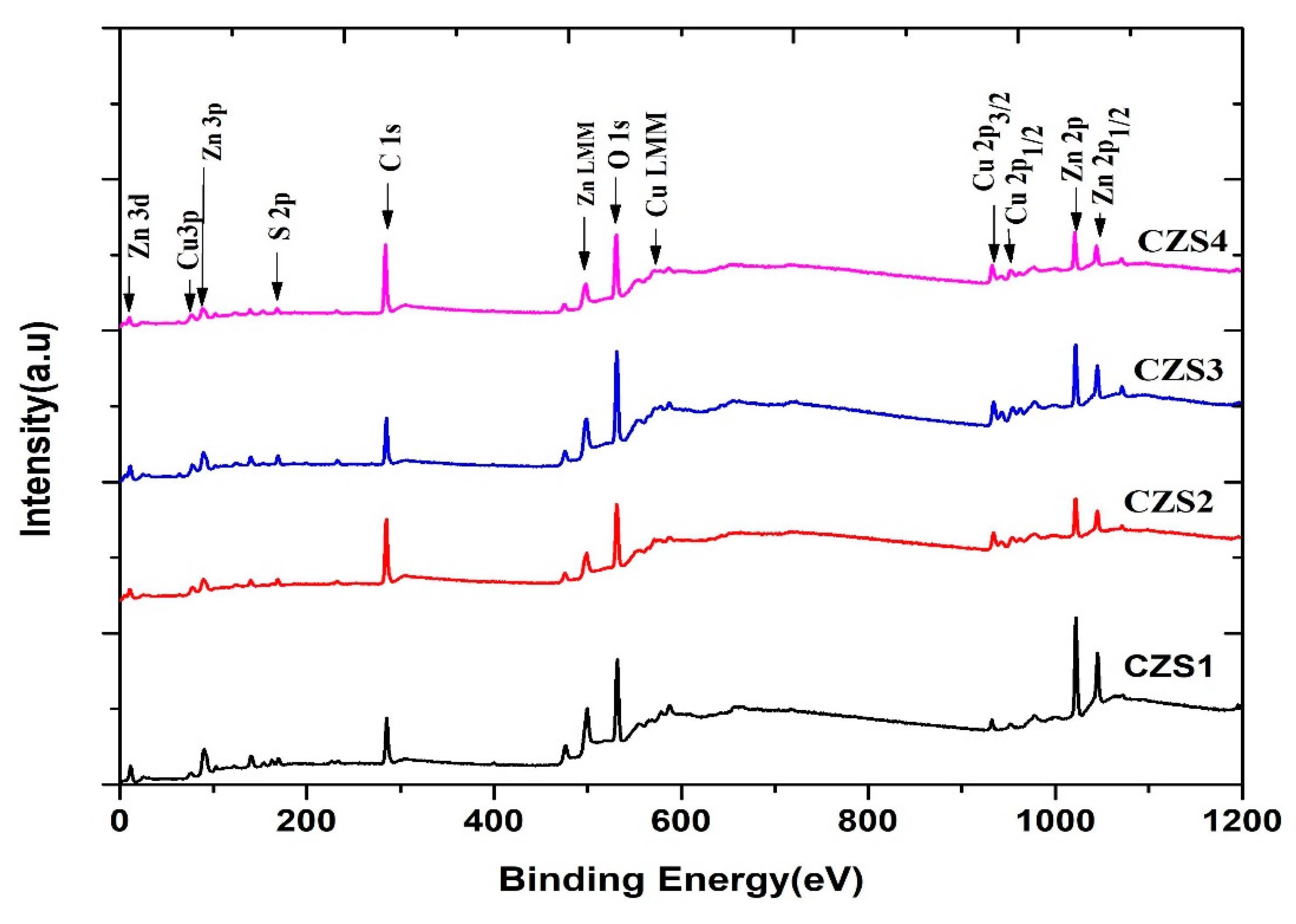
Figure 1: XPS survey and high-resolution core-level spectra of CuZnS thin films (CZS1–CZS4).
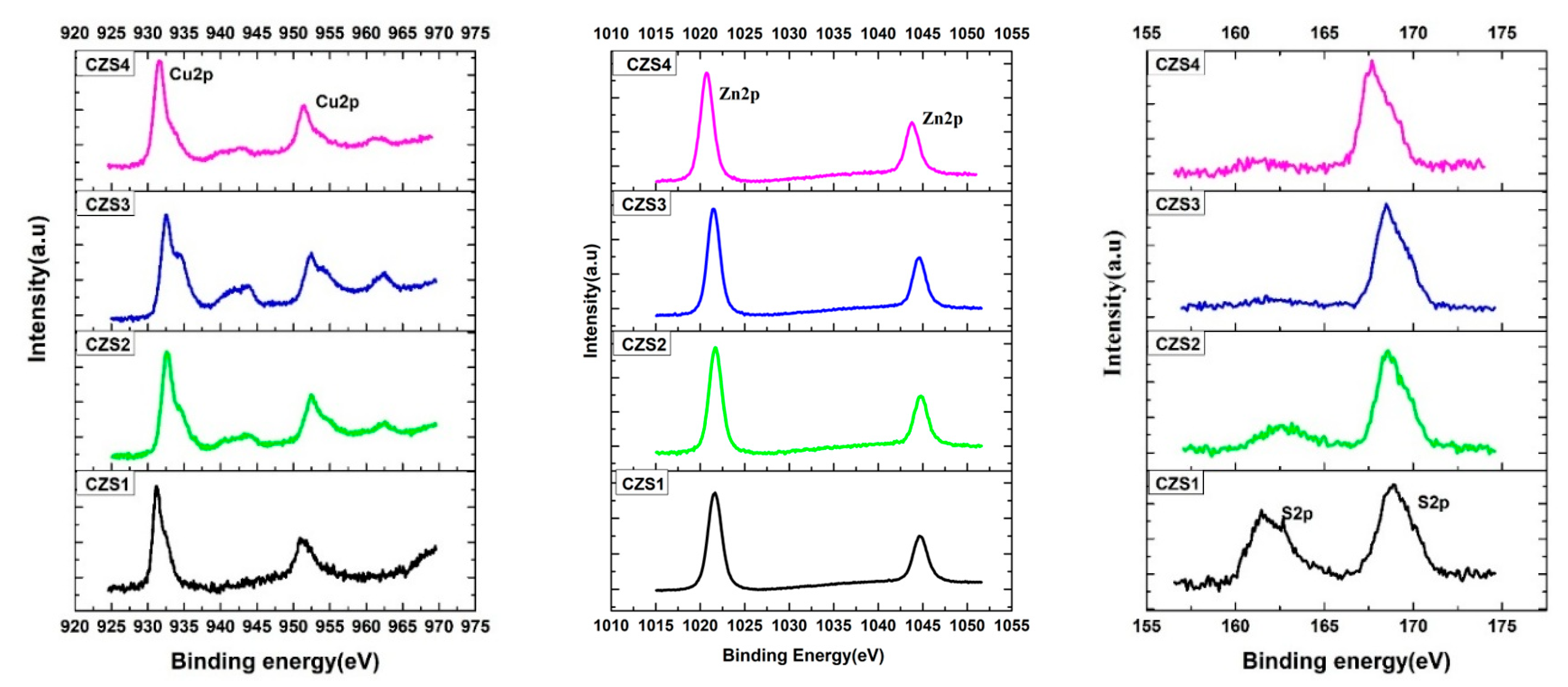
Figure 2: Binding energy distributions of Cu, Zn, and S in CuZnS thin films.
Table 1: Elemental composition (atomic%) of Cu, Zn, and S in CuZnS thin film obtained from XPS analysis.
| Sample Code | Cu Atomic% | Zn Atomic% | S Atomic% | Cu/Zn Ratio |
|---|---|---|---|---|
| CZS1 | 22.43 | 9.73 | 67.84 | 2.30 |
| CZS2 | 28.99 | 11.94 | 59.07 | 2.43 |
| CZS3 | 27.13 | 23.98 | 48.90 | 1.13 |
| CZS4 | 19.84 | 24.17 | 55.19 | 0.82 |
Table 2: Elemental composition (atomic%) of Cu, Zn, and S in CuZnS thin film obtained from EDX analysis.
| Sample Code | Cu Atomic% | Zn Atomic% | S Atomic% | Cu/Zn Ratio |
|---|---|---|---|---|
| CZS1 | 34.27 | 8.43 | 57.30 | 4.06 |
| CZS2 | 20.49 | 39.19 | 40.33 | 0.53 |
| CZS3 | 36.36 | 40.64 | 23 | 0.89 |
| CZS4 | 50.63 | 17.72 | 31.65 | 2.85 |
3.2 Elemental Composition Analysis—Comparison of XPS and EDX
Energy Dispersive X-ray Spectroscopy (EDX) and X-ray Photoelectron Spectroscopy (XPS) were employed to determine the bulk and surface compositions, respectively, of the as-deposited and annealed CuZnS thin films. The quantitative results are summarised in Table 1 and Table 2, comparing both techniques. Both EDX and XPS results reveal a progressive decrease in sulphur content with increasing annealing temperature, accompanied by a relative increase in Zn and Cu concentrations. This compositional shift can be attributed to the thermal desorption of volatile sulphur species at elevated temperatures, leading to a more metal-rich surface. Simultaneously, cation diffusion and rearrangement occur, enabling Zn atoms to occupy thermodynamically stable lattice sites, which enhances overall crystallinity. Notably, the CZS3 sample (annealed at 200°C) exhibits a more balanced cation–anion stoichiometry with a Cu/Zn ratio close to unity (≈1.1 in XPS and 0.89 in EDX). Such a near-stoichiometric composition is advantageous for photovoltaic applications, as it minimises deep defect levels and improves carrier transport within the absorber layer. In contrast, highly Cu-rich or Zn-rich films (e.g., CZS1 and CZS4) may contain antisite or vacancy defects that degrade device efficiency. The discrepancies between XPS and EDX values arise from the difference in analysis depth: XPS probes only the top few nanometers of the film, whereas EDX provides an average bulk composition. Despite these differences, both techniques show consistent compositional trends, validating the observed cation–anion adjustments during annealing. Fig. 3 displays the representative EDX spectrum of the CZS3 sample, confirming the presence of Cu, Zn, and S without detectable impurities. The compositional optimisation achieved in the CZS3 sample supports its improved optoelectronic behaviour, as discussed in the subsequent sections.
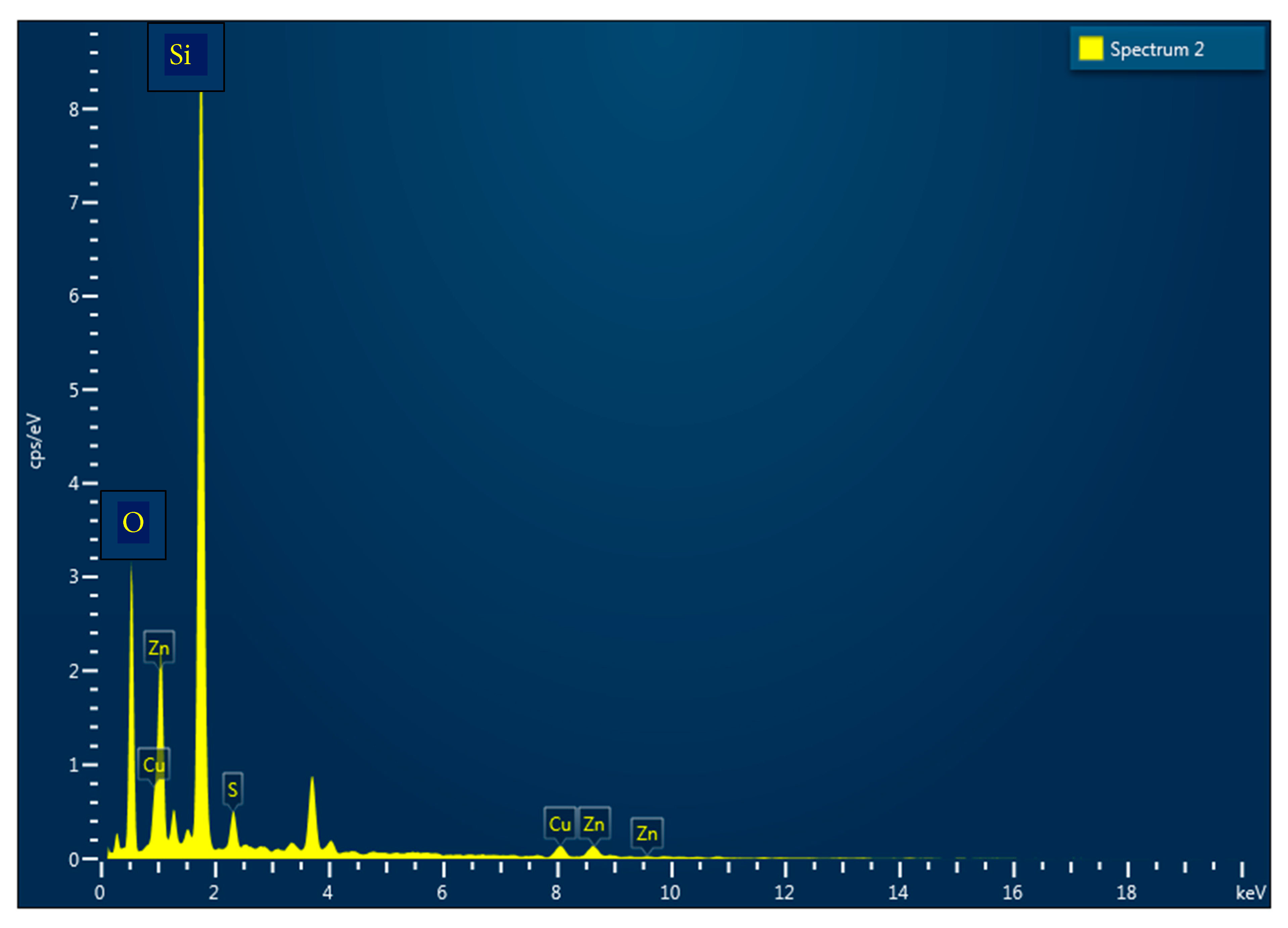
Figure 3: EDX spectrum of CZS3 thin film prepared by CBD method.
3.3 X-Ray Diffraction (XRD) Analysis
X-ray Diffraction (XRD) was employed to study the structural and crystallographic characteristics of the as-deposited and annealed CuZnS thin films [22]. The diffraction patterns were recorded in the 2θ range of 10°–90°, as shown in Fig. 4. The XRD patterns reveal broad and low-intensity peaks, suggesting the formation of nanocrystalline or partially amorphous CuZnS structures. The broadening of diffraction peaks is characteristic of nanocrystallite sizes, which were calculated using the Debye-Scherrer equation.
D = average crystallite size
K = Scherrer constant ~ 0.94 (depends on shape factor)
λ = X-ray wavelength in nm or Å, 1.5406 Å for Cu Kα lines
β = Full width at half maximum of the peak in radians
θ = Bragg angle
The calculated crystallite sizes of all the films were found to be below 5 nm. Such nanoscale crystallites are typical in chemically deposited thin films due to limited adatom mobility during growth. With increasing annealing temperature, a gradual enhancement in peak intensity and a slight reduction in peak broadening were observed, indicating improved crystallinity and reduced lattice disorder. This enhancement can be attributed to thermally induced atomic rearrangements and grain coalescence, which promote more ordered crystalline domains within the film matrix. The characteristic diffraction peaks correspond to the (002) and (022) planes, which are consistent with the reported patterns for cubic CuZnS phases [23,24,25]. The absence of additional impurity peaks confirms the phase purity of the films. Overall, annealing promotes the structural ordering of CuZnS thin films, transforming them from an initially disordered (amorphous-like) state toward improved crystallinity. This enhancement is beneficial for photovoltaic applications, as higher crystallinity reduces defect density and facilitates efficient charge transport.
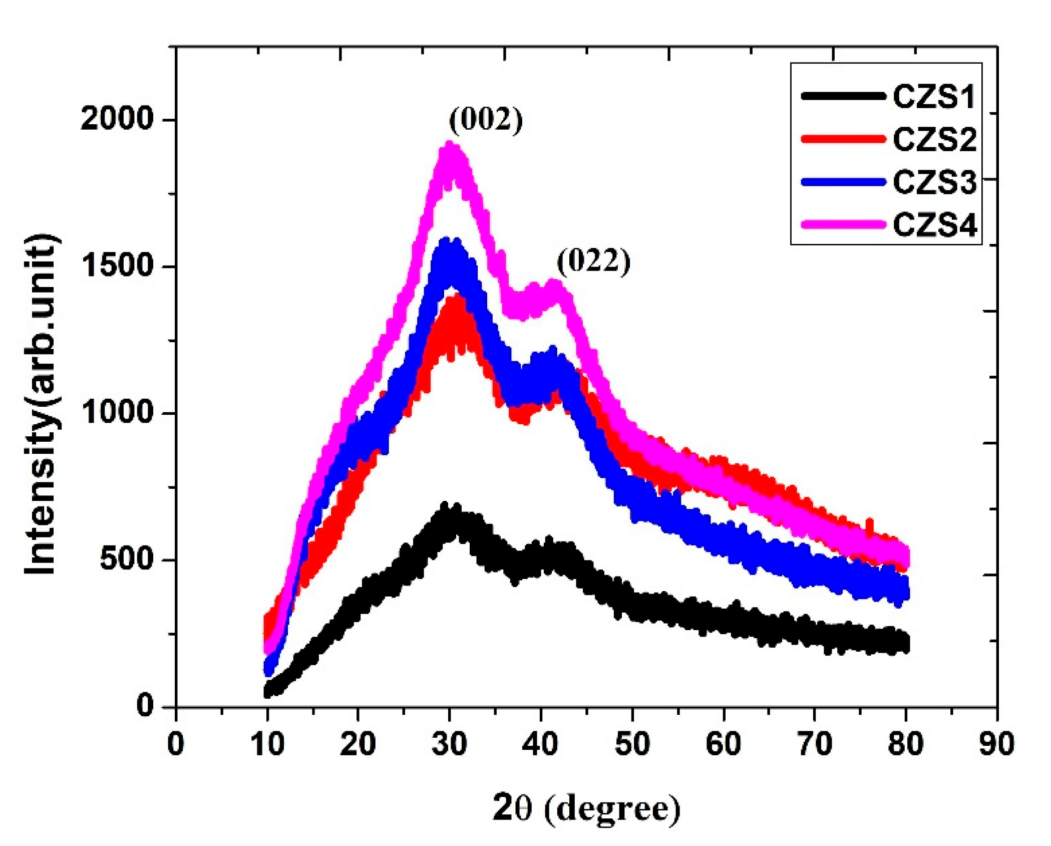
Figure 4: XRD patterns of as-deposited and annealed CuZnS thin films recorded in the 2θ range of 10°–90°, showing the evolution of crystallinity with annealing temperature.
3.4 Scanning Electron Microscopy (SEM)
Scanning Electron Microscopy (SEM) was employed to study the surface morphology and grain evolution of the as-deposited and annealed CuZnS thin films [24,25]. Fig. 5 presents the SEM images of the CZS1, CZS2, CZS3, and CZS4 samples, all recorded with appropriate scale bars for accurate dimensional analysis. The as-deposited film (CZS1) shows a compact surface with densely packed fine grains, while annealed samples display a noticeable increase in grain size and improvement in surface uniformity.
The average grain size was estimated from the SEM micrographs using ImageJ software by measuring the diameters of a statistically significant number of grains selected from different regions of each image, and the mean value was calculated. The grain sizes, summarised in Table 3, range from 149 nm to 178 nm. The CZS3 sample (annealed at 200°C) exhibits the most well-defined spherical grains, indicating enhanced grain coalescence and crystallinity. The surface appears smooth and homogeneous, with fewer voids and grain boundary defects compared to other samples. At higher annealing temperatures (300°C, CZS4), the surface morphology becomes less distinct, and the SEM image appears slightly blurred, suggesting the onset of surface roughening or possible sulphur evaporation, which may lead to non-uniform composition. No cracks or pinholes were observed in any of the samples, confirming the good adhesion and compactness of the films. The observed grain growth upon annealing is attributed to thermally activated diffusion and recrystallisation, which facilitate atomic rearrangement and grain boundary migration. Similar grain enlargement behaviour has been reported for Cu2ZnSnS4 and CuZnS thin films [25,26].
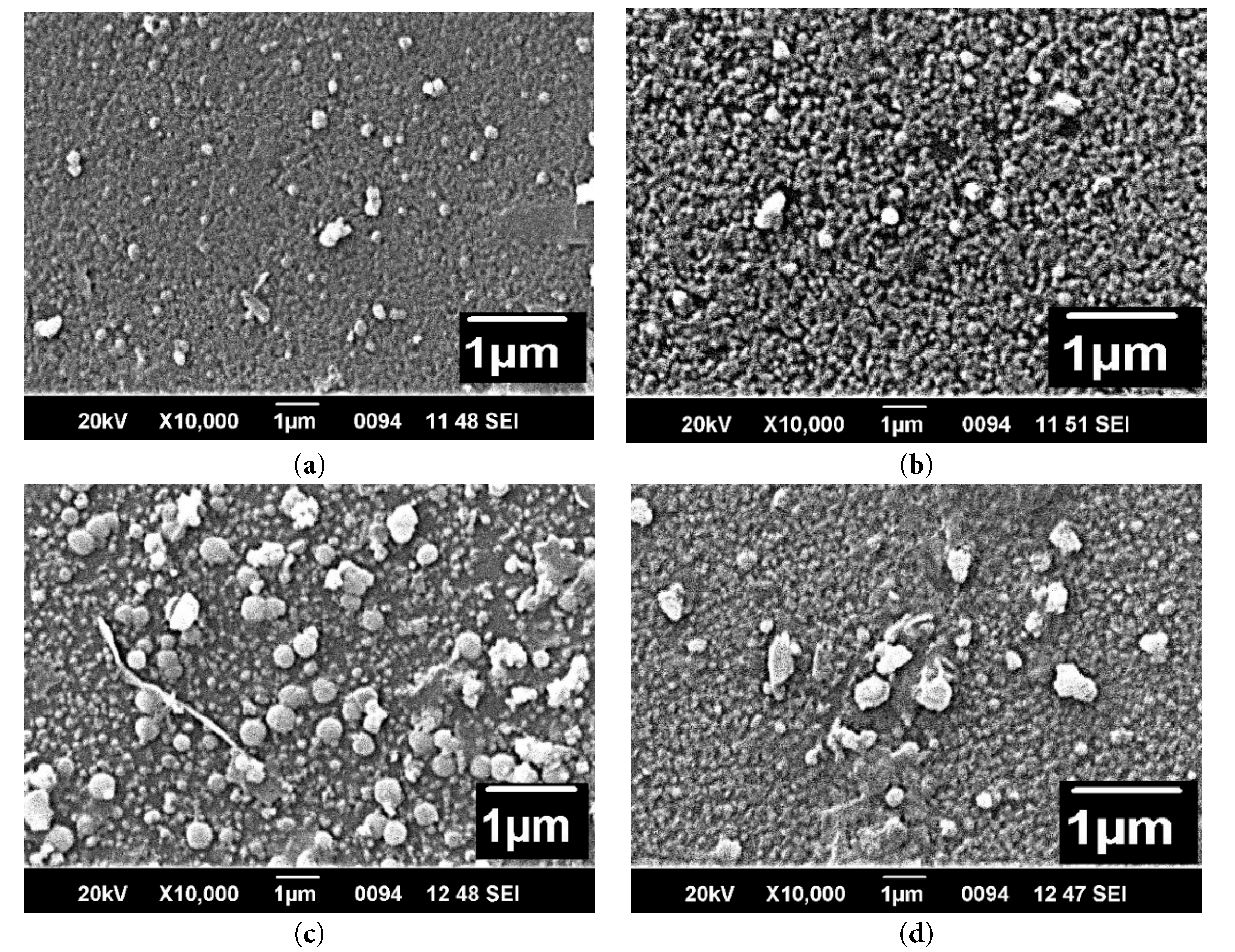
Figure 5: (a–d) represents the sem images of CZS1, CZS2, CZS3, and CZS4 respectively, prepared by the chemical bath deposition method.
Table 3: SEM images of CuZnS thin films (CZS1–CZS4) showing surface morphology evolution and grain growth with annealing temperature.
| Sample Code | Annealing Temperature | Grain Size |
|---|---|---|
| CZS1 | As prepared | 149 nm |
| CZS2 | 100°C | 168 nm |
| CZS3 | 200°C | 178 nm |
| CZS4 | 300°C | 162 nm |
3.5 Optical Properties (UV–Vis Analysis)
Ultraviolet–visible (UV–Vis) spectroscopy was employed to investigate the optical properties of the CuZnS thin films. The optical absorption spectra were recorded in the wavelength range of 300–900 nm, as shown in Fig. 6. The absorption coefficient (α) was calculated from the measured absorbance (A) using the relation
Fig. 7 presents the corresponding Tauc’s plots and direct bandgap estimations for the CZS1–CZS4 thin films. The obtained bandgap values for samples CZS1–CZS4 varied from 2.50 eV to 2.73 eV (Table 4). These values lie within the previously reported range of 1.8–3.6 eV for CuZnS thin films prepared by spray pyrolysis and are consistent with the 2.4–2.6 eV range reported for films grown by the SILAR technique [26,27]. A slight increase in the bandgap with rising annealing temperature was observed. This behaviour can be attributed to several factors, including improved stoichiometry, reduction in defect density, and enhanced crystallinity due to annealing. The loss of sulphur during annealing may also induce slight compositional modifications that influence the electronic band structure. Additionally, the increase in average grain size reduces localised states near the band edges, leading to a modest widening of the bandgap. The optical results confirm that annealing effectively tunes the bandgap energy within the desirable range for photovoltaic absorber layers. The CZS3 film, with an intermediate annealing temperature of 200°C, exhibits a balanced optical response and a suitable bandgap, making it a promising candidate for solar cell applications.
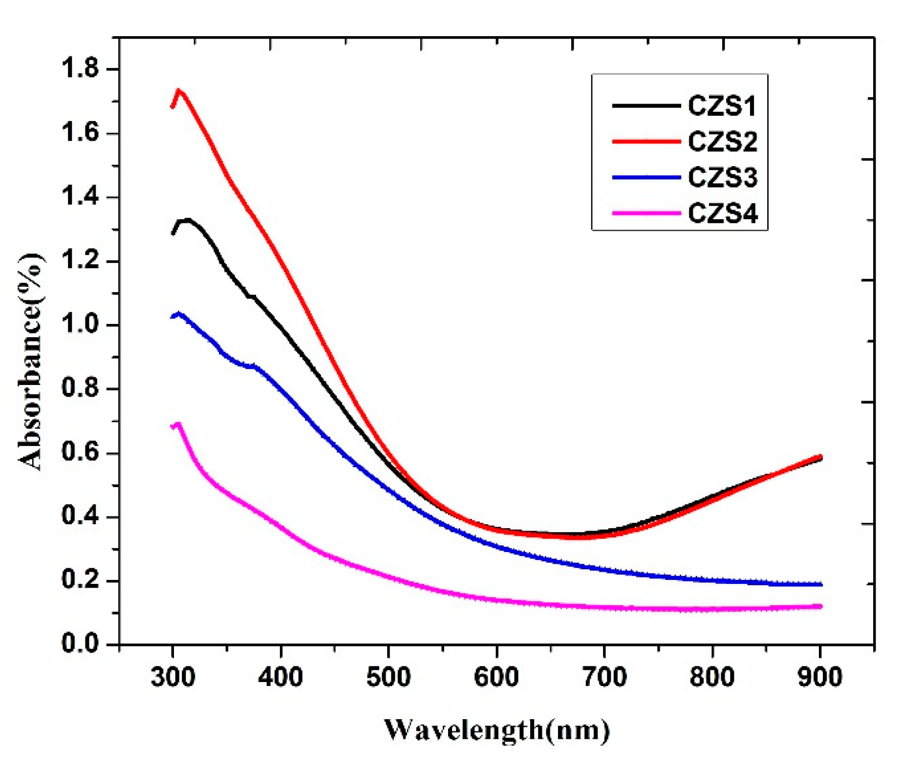
Figure 6: UV–V is absorption spectra of CuZnS thin films (CZS1–CZS4) recorded in the wavelength range 300–900 nm.
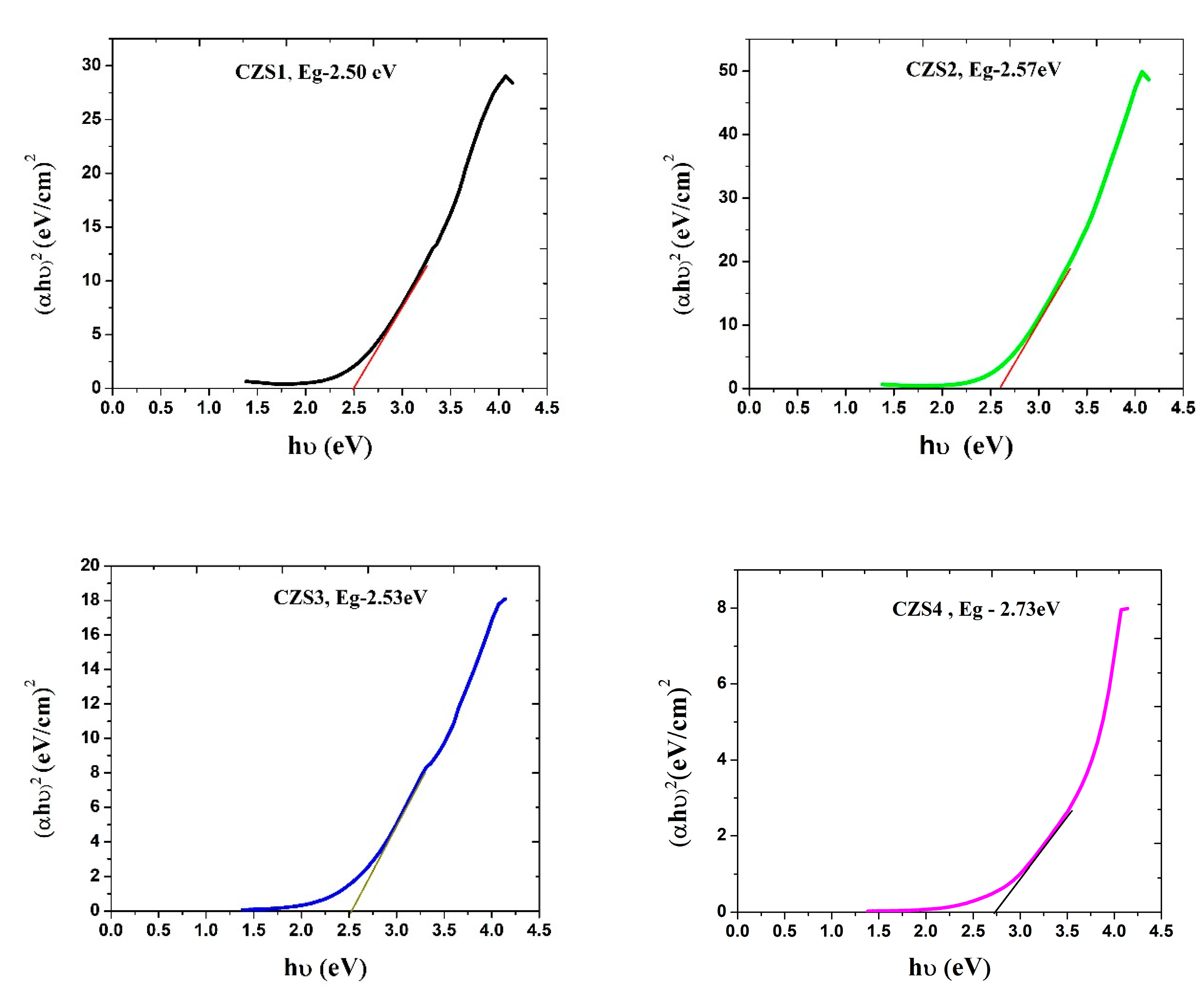
Figure 7: Tauc’s plots of (αhν)2 versus hν for CuZnS thin films (CZS1–CZS4).
Table 4: Optical bandgap (Eg) values of CuZnS thin films (CZS1–CZS4) determined from Tauc’s plots, showing the influence of annealing temperature on bandgap energy.
| Sample Code | Annealing Temperature | Band Gap |
|---|---|---|
| CZS1 | As prepared | 2.50 eV |
| CZS2 | 100°C | 2.57 eV |
| CZS3 | 200°C | 2.53 eV |
| CZS4 | 300°C | 2.73 eV |
3.6 Electrical Properties (Hall Measurements)
The Hall effect measurement is a reliable and widely adopted technique for evaluating the electrical properties of semiconductor thin films. Table 5 presents the Hall parameters of the CuZnS thin films (CZS1–CZS4). Among the samples, CZS1, CZS2, and CZS3 exhibit p-type conductivity, while CZS4 shows a transition to n-type behaviour. The results indicate that with increasing annealing temperature, the bulk carrier concentration and sheet resistance decrease, whereas carrier mobility and electrical conductivity increase. These enhancements can be attributed to improved crystallinity, reduced defect density, and better atomic ordering induced by annealing.
According to the literature, CuZnS thin films generally exhibit carrier concentrations in the range of 1017–1020 cm−3, carrier mobility between 0.1–10 cm2 V−1 s−1, and conductivity values between 0.01 and 20 S cm−1 [28,29,30,31,32]. In the present study, the measured carrier concentration is of the order of ~1013 cm−3, which is lower than the typical range, while the mobility values are comparable to the reported values. Although the conductivity (~10−6 S cm−1) is lower than that reported for heavily doped or non-stoichiometric films, such behaviour is characteristic of wide-bandgap semiconductors with low intrinsic carrier concentration. From a device perspective, lower carrier concentration can be advantageous in absorber layers by reducing recombination losses and enhancing charge separation, provided sufficient carrier mobility is maintained. In this context, the relatively stable mobility values observed in the present study suggest that charge transport is not severely hindered. Among all samples, CZS3 (annealed at 200°C) exhibits the most balanced combination of carrier concentration, mobility, and conductivity, indicating its potential suitability for photovoltaic and optoelectronic applications.
Table 5: Hall effect parameters of CuZnS thin films (CZS1–CZS4) showing the influence of annealing temperature on carrier type, concentration, mobility, and conductivity.
| Sample Code | Bulk Concentration (×1013 cm−3) | Mobility cm2/Vs | Sheet Resistance (×1010 Ω/sq.area) | Conductivity (×10−6 Ω−1 cm−1) | Av.Hall Coefficient (×104 cm3/c) | Conductivity Type |
|---|---|---|---|---|---|---|
| CZS1 | 7.87 | 0.18 | 5.41 | 2.31 | 7.92 | p |
| CZS2 | 6.25 | 0.24 | 6.45 | 2.46 | 9.98 | p |
| CZS3 | 1.15 | 2.92 | 2.89 | 5.40 | 54.18 | p |
| CZS4 | −4.15 | 1.11 | 1.61 | 7.40 | −15.04 | n |
CuZnS thin films were successfully synthesised using the chemical bath deposition (CBD) technique, and both as-deposited and annealed samples were systematically characterised. XPS analysis confirmed the presence of Cu, Zn and S elements and revealed that Cu and Zn contents increase, whereas sulphur content decreases with annealing, leading to a reduced Cu/Zn ratio at higher annealing temperatures. Among the samples, CZS3 exhibited a more balanced elemental composition with atomic percentages of Cu: 27.13%, Zn: 23.98%, and S: 48.90%. The elemental distribution obtained from XPS and EDX analyses showed good agreement, confirming the compositional consistency of the films.
XRD analysis indicated that the as-prepared films possess an amorphous nature with nanosized crystallites, as inferred from peak broadening. Upon annealing, the diffraction peaks became more intense and sharper, reflecting enhanced crystallinity and structural ordering. The prominent (002) and (022) planes were identified in the diffraction patterns. SEM micrographs revealed improved surface morphology and grain growth with annealing, with grain size increasing from 149 nm to 178 nm. Optical characterisation using UV–Vis spectroscopy showed that the bandgap energy varied between 2.50 eV and 2.73 eV. A slight decrease in bandgap with increasing annealing temperature was attributed to enhanced crystallinity and increased grain size, both of which reduce defect-related localised states near the band edges. Hall effect measurements confirmed that the films exhibit p-type conductivity, with carrier mobility in the range of 0.18–2.92 cm2 V−1 s−1 comparable to reported values for CuZnS semiconductors. The measured bulk carrier concentration (~1013 cm−3) and conductivity (~10−6 S cm−1) were lower than standard literature values, though both parameters improved upon annealing, likely due to improved microstructural quality.
Overall, the sample annealed at 200°C (CZS3) demonstrated the most favourable balance of composition, optical properties, and electrical characteristics, making it a promising candidate for further investigation in photovoltaic applications. Despite these promising results, the present study is limited to material-level characterisation, and no device fabrication or long-term stability assessment has been performed. Future work will focus on this direction.
Acknowledgement:
Funding Statement: The authors received no specific funding for this study.
Author Contributions: The authors confirm their contribution to the paper as follows: study conception and design: Preetha K. C., Bini S.; analysis and interpretation of results: Preetha K. C., Bini S.; draft manuscript preparation: Preetha K. C., Bini S. All authors reviewed and approved the final version of the manuscript.
Availability of Data and Materials: Not applicable.
Ethics Approval: Not applicable.
Conflicts of Interest: The authors declare no conflicts of interest.
References
1. Kavita SJ , Nanasaheb H . Investigation of Optical and Electrical Properties of CuZnS Thin Film Deposited by Chemical Bath Deposition Method. Innov Res Sci Eng Technol. 2021; 10( 8): 2347– 6710. doi:10.15680/IJIRSET.2021.1008185 [Google Scholar] [CrossRef]
2. Gubari GMM , Ibrahim Mohammed SM , Huse NP , Dive AS , Sharma R . An experimental and theoretical study of Cu0.2Zn0.8S thin film grown by facile chemical bath deposition as an efficient photosensor. J Electron Mater. 2018; 47( 10): 6128– 35. doi:10.1007/s11664-018-6491-3. [Google Scholar] [CrossRef]
3. Sreejith MS , Deepu DR , Kartha CS , Rajeevkumar K , Vijayakumar KP . Tuning the properties of sprayed CuZnS films for fabrication of solar cell. Appl Phys Lett. 2014; 105( 20): 202107. doi:10.1063/1.4902224. [Google Scholar] [CrossRef]
4. Jubimol J , Sreejith MS , Kartha CS , Vijayakumar KP , Louis G . Analysis of spray pyrolysed copper zinc sulfide thin films using photoluminescence. J Lumin. 2018; 203: 436– 40. doi:10.1016/j.jlumin.2018.06.079. [Google Scholar] [CrossRef]
5. Uhuegbu CC , Babatunde EB . Spectral analysis of copper zinc sulphide ternary thin film grown by solution growth technique. Am J Sci Ind Res. 2010; 1( 3): 397– 400. doi:10.5251/ajsir.2010.1.3.397.400. [Google Scholar] [CrossRef]
6. Fernando WTRS , Jayathilekea KMDC , Wijesundera RP , Siripala W . Growth of CuZnS thin films for PV applications. Proc Tech Sess. 2017; 33: 12– 8. [Google Scholar]
7. Ezenwa IA , Okoli NL . Characterization of chemically synthesized copper zinc sulphide (CuZnS2) thin films. Eur Open Appl Phys J. 2015; 1( 1): 1– 9. [Google Scholar]
8. Choi JY , Kim KJ , Yoo JB , Kim D . Properties of cadmium sulfide thin films deposited by chemical bath deposition with ultrasonication. Sol Energy. 1998; 64( 1–3): 41– 7. doi:10.1016/S0038-092X(98)00047-4. [Google Scholar] [CrossRef]
9. Nair PK , Nair MS , Fernandez A , Ocampo M . Prospects of chemically deposited metal chalcogenide thin films for solar control applications. J Phys D Appl Phys. 1989; 22( 6): 829– 36. doi:10.1088/0022-3727/22/6/021. [Google Scholar] [CrossRef]
10. Ali Yildirim M , Ateş A , Astam A . Annealing and light effect on structural, optical and electrical properties of CuS, CuZnS and ZnS thin films grown by the SILAR method. Phys E Low Dimension Syst Nanostruct. 2009; 41( 8): 1365– 72. doi:10.1016/j.physe.2009.04.014. [Google Scholar] [CrossRef]
11. Ali J , Bushra KH . Fabrication and study structure and optical properties of Cu0.75Zn0.25S Thin Film, Ibn AL-Haitham. J Pure Appl Sci. 2025; 38( 2): 184– 93. doi:10.30526/38.2.4022. [Google Scholar] [CrossRef]
12. Souza HJD , D’Souza N , Ashith VK , Nagappa Moger S , D’Silva ED . Effect of deposition time on copper incorporation of ZnS thin films by low-cost technique. Mater Sci Eng B. 2023; 294: 116551. doi:10.1016/j.mseb.2023.116551. [Google Scholar] [CrossRef]
13. Huse NP , Patil RM , Sharma R . Characterization of economic and non-toxic copper doped zinc sulfide thin film grown by facile chemical bath deposition method. ES Mater Manuf. 2023; 20: 839. doi:10.30919/esmm5f839. [Google Scholar] [CrossRef]
14. Lv Z , Yan S , Mu W , Liu Y , Xin Q , Liu Y , et al. A high responsivity and photosensitivity self-powered UV photodetector constructed by the CuZnS/Ga2O3 heterojunction. Adv Mater Interfaces. 2023; 10( 5): 2202130. doi:10.1002/admi.202202130. [Google Scholar] [CrossRef]
15. Preetha KC , Bini S . Structural, morphological, compositional, electrical, and optical characterizations of CuZnS thin films prepared using chemical bath deposition method. J Cond Matt. 2025; 3( 2): 128– 32. doi:10.61343/jcm.v3i02.77. [Google Scholar] [CrossRef]
16. Sundaram SK , Subramanian S , Panneerselvam V , Salammal ST . Temperature-dependent phase transition of CuZnS thin films and its effects on morphological, optical and electrical properties. Thin Solid Films. 2021; 733: 138810. doi:10.1016/j.tsf.2021.138810. [Google Scholar] [CrossRef]
17. Soud AJ , Al-Maiyaly BKH . Nano crystalline Cu0.25Zn0.75S thin films properties dependent on annealing temperature. In: Proceedings of the 6th International Conference for Physics and Advance Computation Sciences; 2024 Aug 26–27; Baghdad, Iraq. doi:10.1063/5.0265879. [Google Scholar] [CrossRef]
18. Li L , Zhu P , Peng S , Srinivasan M , Yan Q , Nair AS , et al. Controlled growth of CuS on electrospun carbon nanofibers as an efficient counter electrode for quantum dot-sensitized solar cells. J Phys Chem C. 2014; 118( 30): 16526– 35. doi:10.1021/jp4117529. [Google Scholar] [CrossRef]
19. Güneri E , Kariper A . Optical properties of amorphous CuS thin films deposited chemically at different pH values. J Alloys Compd. 2012; 516: 20– 6. doi:10.1016/j.jallcom.2011.11.054. [Google Scholar] [CrossRef]
20. Jiang X , Wong FL , Fung MK , Lee ST . Aluminum-doped zinc oxide films as transparent conductive electrode for organic light-emitting devices. Appl Phys Lett. 2003; 83( 9): 1875– 7. doi:10.1063/1.1605805. [Google Scholar] [CrossRef]
21. Tang D , Wang Q , Liu F , Zhao L , Han Z , Sun K , et al. An alternative route towards low-cost Cu2ZnSnS4 thin film solar cells. Surf Coat Technol. 2013; 232: 53– 9. doi:10.1016/j.surfcoat.2013.04.052. [Google Scholar] [CrossRef]
22. Dubale DG , Abshiro TA , Hone FG . Synthesis and characterization of copper zinc sulfide (CuxZn1−xS) ternary thin film by using acidic chemical bath deposition method. Int J Thin Films Sci Technol. 2021; 10( 1): 21– 7. doi:10.18576/ijtfst/100104. [Google Scholar] [CrossRef]
23. Aghaei F , Sahraei R , Soheyli E , Daneshfar A . Dopant-Concentration Dependent Optical and Structural Properties of Cu-Doped ZnS Thin Films. J Nanostruct. 2022; 12( 2): 330– 42. doi:10.22052/JNS.2022.02.010. [Google Scholar] [CrossRef]
24. Omran Alkhayatt AH , AbdulWahab Habieb A , Hadi Abbas Al-Noaman A , Abdulhussein Hameed A . Structure, surface morphology and optical properties of CuxZn1−xS/Au NPs layer for photodetector application. J Phys Conf Ser. 2019; 1234( 1): 012012. doi:10.1088/1742-6596/1234/1/012012. [Google Scholar] [CrossRef]
25. Nadi SA , Chelvanathan P , Zakaria Z , Alam MM , Alothman ZA , Sopian K , et al. Postdeposition annealing effect on Cu2ZnSnS4Thin films grown at different substrate temperature. Int J Photoenergy. 2014; 2014: 589027. doi:10.1155/2014/589027. [Google Scholar] [CrossRef]
26. Kitagawa N , Ito S , Nguyen DC , Nishino H . Copper zinc sulfur compound solar cells fabricated by spray pyrolysis deposition for solar cells. Nat Resour. 2013; 4( 1): 142– 5. doi:10.4236/nr.2013.41a018. [Google Scholar] [CrossRef]
27. Jose E , Santhosh Kumar MC . Room temperature deposition of highly crystalline Cu-Zn-S thin films for solar cell applications using SILAR method. J Alloys Compd. 2017; 712: 649– 56. doi:10.1016/j.jallcom.2017.04.097. [Google Scholar] [CrossRef]
28. Cabrera-German D , Martínez-Gil M , Fuentes-Ríos L , Montiel-González Z , Mazón-Montijo DA , Sotelo-Lerma M . Insights into the SILAR processing of CuxZn1−xS thin films via a chemical, structural, and optoelectronic assessment. ACS Omega. 2023; 8( 50): 48056– 70. doi:10.1021/acsomega.3c06848. [Google Scholar] [CrossRef]
29. Mallick A , Chattopadhyay S , De G , Basak D . High figure of merit p-type transparent conducting thin film based on solution processed CuS-ZnS nanocomposite. J Alloys Compd. 2019; 770: 813– 22. doi:10.1016/j.jallcom.2018.08.178. [Google Scholar] [CrossRef]
30. Woods-Robinson R , Han Y , Mangum JS , Melamed CL , Gorman BP , Mehta A , et al. Combinatorial tuning of structural and optoelectronic properties in Cu Zn1–S. Matter. 2019; 1( 4): 862– 80. doi:10.1016/j.matt.2019.06.019. [Google Scholar] [CrossRef]
31. Woods-Robinson R , Cooper JK , Xu X , Schelhas LT , Pool VL , Faghaninia A , et al. P-type transparent Cu-alloyed ZnS deposited at room temperature. Adv Elect Mater. 2016; 2( 6): 1500396. doi:10.1002/aelm.201500396. [Google Scholar] [CrossRef]
32. Xu X , Bullock J , Schelhas LT , Stutz EZ , Fonseca JJ , Hettick M , et al. Chemical bath deposition of p-type transparent, highly conducting (CuS)x:(ZnS)1-x nanocomposite thin films and fabrication of Si heterojunction solar cells. Nano Lett. 2016; 16( 3): 1925– 32. doi:10.1021/acs.nanolett.5b05124. [Google Scholar] [CrossRef]
Cite This Article
 Copyright © 2026 The Author(s). Published by Tech Science Press.
This work is licensed under a Creative Commons Attribution 4.0 International License , which permits unrestricted use, distribution, and reproduction in any medium, provided the original work is properly cited.
 Downloads
 Citation Tools