
 Submit a Paper
 Propose a Special lssue
 Open Access
ARTICLE
Analyzing the ZnO and CH3NH3PbI3 as Emitter Layer for Silicon Based Heterojunction Solar Cells
1 Renewable Energy Source Laboratory, Andijan State University, Uzbekistan
2 College of Engineering and Technology, American University of the Middle East, Kuwait
* Corresponding Author: Jasurbek Gulomov. Email:
Computers, Materials & Continua 2023, 74(1), 575-590. https://doi.org/10.32604/cmc.2023.031289
Received 14 April 2022; Accepted 21 June 2022; Issue published 22 September 2022
 View Full Text
 Download PDF
Abstract
Today, it has become an important task to modify existing traditional silicon-based solar cell factory to produce high-efficiency silicon-based heterojunction solar cells, at a lower cost. Therefore, the aim of this paper is to analyze CH3NH3PbI3 and ZnO materials as an emitter layer for p-type silicon wafer-based heterojunction solar cells. CH3NH3PbI3 and ZnO can be synthesized using the cheap Sol-Gel method and can form n-type semiconductor. We propose to combine these two materials since CH3NH3PbI3 is a great light absorber and ZnO has an optimal complex refractive index which can be used as antireflection material. The photoelectric parameters of n-CH3NH3PbI3/p-Si, n-ZnO/p-Si, and n-Si/p-Si solar cells have been studied in the range of 20–200 nm of emitter layer thickness. It has been found that the short circuit current for CH3NH3PbI3/p-Si and n-ZnO/p-Si solar cells is almost the same when the emitter layer thickness is in the range of 20–100 nm. Additionally, when the emitter layer thickness is greater than 100 nm, the short circuit current of CH3NH3PbI3/p-Si exceeds that of n-ZnO/p-Si. The optimal emitter layer thickness for n-CH3NH3PbI3/p-Si and n-ZnO/p-Si was found equal to 80 nm. Using this value, the short-circuit current and the fill factor were estimated around 18.27 mA/cm2 and 0.77 for n-CH3NH3PbI3/p-Si and 18.06 mA/cm2 and 0.73 for n-ZnO/p-Si. Results show that the efficiency of n-CH3NH3PbI3/p-Si and n-ZnO/p-Si solar cells with an emitter layer thickness of 80 nm are 1.314 and 1.298 times greater than efficiency of traditional n-Si/p-Si for the same sizes. These findings will help perovskites materials to be more appealing in the PV industry and accelerate their development to become a viable alternative in the renewable energy sector.Keywords
85% of the solar cells produced in the industry are made from silicon [1]. However, the efficiencies of these silicon solar cells do not exceed 29%, according to Shockley-Quiesser theory [2], and this is mainly due to electrical, thermal and optical losses in the silicon solar cells. Losses by reflection between the incident light and the front surface of silicon solar cell account for more than 30%. [3]. Due to surface defects, the amount of Shockley-Read-Hall SRH recombination on the surface of the solar cell is greater than the volume itself, which is known as surface recombination. In order to improve the solar cell efficiency and reduce the reflection coefficient and surface recombination, the front surface of the silicon solar cells is usually covered with two layers of SiNx and SiO2, with a thickness of 75 and 100 nm, respectively. If the solar cell’s thickness is thin, the photogeneration rate will increase at its rear side, leading to an increase of the surface recombination which makes it active [4]. Therefore, the rear side of thin film silicon solar cell is covered with SiNx, Al2O3 or SiO2 materials, which have passivation properties in the active regions [5]. Gradient refractive index is made from some antireflection coatings to optimize the optical properties of solar cells [6]. Additionally, creating the pyramidal textures with a base angle of 70.4° on the front surface of silicon solar cell was proposed by [6] to lower the reflection coefficient of solar cells and to improve the absorption coefficient of photons [7]. Since the silicon solar cells absorb light in the visible spectrum range [8], luminescent materials [9] and quantum dots [10] are formed on the surface of the solar cell to extend absorption spectrum. In addition, with the introduction of metal nanoparticles into the n region of silicon solar cells, the photoelectric parameters were improved [11].
In the race of conversion efficiency, perovskite solar cells turned out to be a valuable solution. Their efficiency has increased from about 3% in 2006 to over 25% today [12]. Perovskite materials are crystal with ABX3 structure, where A and B are cations and X is anion. In fact, there are three main-types of crystal structure in perovskites: cubic, tetragonal and orthorhombic. Orthorhombic-tetragonal-cubic phase transitions were investigated experimentally and analyzed theoretically in [13]. Perovskites offer high absorption coefficient, which makes it useful as absorber materials. Consequently, inorganic and inorganic-organic hybrid perovskite materials are employed in photovoltaic cells mainly because lead halide perovskites are far more convenient materials for solar cells. According to Shockley-Queissier theory, the upper limit efficiency of a single junction CH3NH3PbI3 based solar cells is 31% [14]. Silicon or other traditional semiconductor based single junction solar cells can reach their theoretical maximum efficiency for a thickness of 150–300 μm. However, by changing the surface morphology of CH3NH3PbI3 based solar cells, the theoretical Shockley-Quiesser limit can be achieved with a thickness of 200 nm [15].
CH3NH3PbI3 offers many advantages over GaAs. First of all, it is a direct semiconductor. Secondly, it can be easily manufactured, at better cost when compared to GaAs and lastly, both options offer similar band gap energies.
In order to enhance the performance of perovskite solar cells, TiO2, ZnO and SnO2 can be employed as an electron transport layer (ETL) and Cu2O, NiOx, spiro-OMeTAD as a hole transport layer (HTL). Thus, when combining these advantages, CH3NH3PbI3/Si tandem solar cell are recommended to increase the conversion efficiency. In theory, [16] CH3NH3PbI3/Si solar cells efficiency are unable to surpass 46.1% while [17] reported an attained efficiency of 27.9%.
The advantages made the use of perovskite materials an appealing subject of research. Nerveless, perovskite materials are used in parallel with metal oxides due to their transparent and semiconductor properties, their abundance and their low-cost synthesis. In this regard, metal oxides are used as an ETL and HTL for perovskite solar cells. The most common metal oxides used with perovskite materials are TiO2, ZnO, SnO2, NiOx, Cu2O and CuO [18]. They can be divided into two categories, depending on their tendency to be n or p-type semiconductors. In fact, creating n-type semiconductors from TiO2, ZnO, SnO2, CuO and p-type semiconductors from Cu2O, NiOx are simple and straightforward during synthesis process. Given that buildings generate more than 40% of the annual global CO2 emission, transparent solar cells made from metal oxides are proposed as facade and windows, to decrease greenhouse emissions and help achieve the sustainable development goals 7 and 13, related to clean energy and climate action. Yet, these metal oxides solar cells have limitations, mainly because of their low efficiency. For instance, the efficiency of n-ZnO/p-NiOx heterojunction solar cell was experimentally estimated around 0.542% by [19].
CH3NH3PbI3 and ZnO can be synthesized by using the same Sol-Gel method. In industry, most of solar cell manufacturing factories are customized to produce mono or poly-crystal silicon wafer based solar cells. Traditional silicon solar cells are produced following 10 steps in manufacturing [20]. During the second step of manufacturing, p-n junction is formed by adding Phosphorous atoms to p-type silicon wafer. It is possible to produce p-type silicon-based heterojunction solar cells while only adjusting the second step of production. Then, during the second step of manufacturing, p-n heterojunction should be formed by addition of CH3NH3PbI3 or ZnO on p-type silicon wafer, using Sol-gel method. This is feasible due to the band gap energy of CH3NH3PbI3 (1.56 eV) and ZnO (3.3 eV) which are greater than the band gap energy of silicon (1.12 eV). Consequently, when heterojunction is formed on p-type silicon wafer, the absorption spectrum and the photoelectric parameters of solar cells are improved. Similarly, the quality of heterojunctions depends on the material and the type of emitter layer. Therefore, the aim of this study is to investigate, using numerical simulation, the use of CH3NH3PbI3 and ZnO as emitter layer of p-type silicon based solar cell and study the impact of their thicknesses on photoelectric parameters.
We opt for the simulation approach to investigate silicon-based heterojunction cells. In general, simulating such cells is more complex than other semiconductors, since more computing power is required to simulate the optic and electrical properties with high accuracy. Several software offer solar cells simulation, among which, the most being used are Silvaco TCAD, Lumerical TCAD and Sentaurus TCAD. Sentaurus TCAD was the software we used in our studies, since it is the most appropriate for our simulations. Good agreement between numerical and experimental results was achieved in our TCAD simulations. Sentaurus TCAD consists of 17 main tools, and 4 additional tools. In this paper, only four main tools have been used to simulate solar cells which are Sentaurus Structure Editor, Sentaurus Device, Sentaurus Visual and Sentaurus Workbench. Sentaurus Structure Editor is utilized to create geometric model of semiconductor devices. Information about creating geometric models of solar cells in Sentaurus Structure Editor by using Tool Command Language (TCL) was given in [21]. For the sake of this paper, we used TCL algorithms to generate the geometric model of our solar cells. Furthermore, we used 2D modeling to obtain accurate and fast calculations, assuming that our solar cell model is symmetrical. Besides, AM1.5 light spectrum is used as a light source in our simulations. n-ZnO/p-Si, n-CH3NH3PbI3/p-Si, and n-Si/p-Si solar cells have been simulated to evaluate their performance. Therefore, the same geometrical sizes and doping concentrations for both solar cells were considered. As for the thicknesses of the emitter and the base, they were set to 200 nm and 9 μm, with a width of 10 μm. In addition, concentrations of donor in emitter region and acceptor in base region are 1.1017 cm−3 and 1.1015 cm−3, respectively. In Fig. 1, the geometric and band structures of n-ZnO/p-Si (a) and n-CH3NH3PbI3/p-Si (b) heterojunction solar cells are shown. After creating the geometric models, each material properties are given with parameter files to respective regions.

Figure 1: Geometric structure and band structure of n-ZnO/p-Si (a) and n-CH3NH3PbI3/p-Si (b) heterojunction solar cells. ltot = 10 μm, lc = 0.5 μm, de = 20÷200 nm, dh = 10 μm
The main physical parameters of materials are: complex refractive index, band gap, electron affinity, density of states in conduction and valence band, electron and hole effective masses, permittivity, ionization energy of doping atoms, radiative recombination coefficient, Auger recombination coefficients, lattice heat capacity, thermal conductivity as well as fitting parameters for mobility models. Assigning material properties to specific regions is performed in Sentaurus Device. Sentaurus Device has a large material database, which includes elementary, binary, ternary semiconductors, metals and insulators. The database related to silicon in Sentaurus Device is quite extensive, and validated experimentally. However, parameter files of metal oxides such as ZnO as well as perovskites (CH3NH3PbI3) are not available. This is why, we collected the necessary physical parameters of ZnO and CH3NH3PbI3 from reliable experimental resources.
2.2 Physical Properties of ZnO
ZnO is one of the most used metal oxides. It is utilized to create optical transparent devices due to its transparency and wide band gap (3.3 eV). In addition, it has a high exciton binding energy (60 meV) and by consequence, it is available to create a single crystal. Methods used to synthesize ZnO fall into three main categories: chemical, biological and physical. Synthesis method strongly impacts the properties of ZnO. The easiest synthesis method of ZnO is the Sol-Gel, which is chemical. Thus, we decided to use the properties of ZnO grown by Sol-Gel method in our simulations since it allows the deposition of ZnO on the silicon wafer using Sol-Gel method. In modeling, it is crucial to choose the correct main materials’ parameters. Therefore, in the collection of physical parameters of ZnO, we focused on the method of its production and the compatibility of the experimental results with literatures [22–28]. The band gap energy of ZnO, given in the literature, ranges from 3.2 to 3.5 eV. In semiconductor materials, the Varshni empiric formula expresses the relation between the band gap energy and the temperature of the crystal. This relation is expressed in Eq. (1) below:
Eg(T) is the band gap energy at T(K), Eg(0) is the band gap energy at 0 K, T is temperature, α and β are the fitting parameters.
Varshni’s correlation is an empirical formula, and the correction coefficients and the initial values are fitted from experimental data. Yue Li Song estimated the band gap energy of ZnO as a function of temperature, then he analyzed statistically the coefficients mentioned which were found equal to Eg(0) = 3.394 eV, α = 0.22 meV/K and β = 175.8 K, of Varshni formula for ZnO [22]. Since ZnO has a direct wide band gap, it generates hot electrons and holes when it absorbs photons with high energy. Due to the electron-phonon interaction, relaxation of electron energy is manifested. In Emilis’s experiments, energy relaxation times for electron and holes are 0.84 ps and 0.15 ps, respectively [23]. In Sol-Gel method, it is simple to synthesize Al-doped ZnO by using Zn(CH3COO)2⋅2H2O and Al(OH)(CH3COO)2 [24]. Ionization energy of Al atoms in ZnO crystal equals to 0.054 eV [25]. Density of states for ZnO are equal to 2.2.1018 cm−3 in conduction band and 1.8.1019 cm−3 in valence band [26]. Klaus Ellmer adapted mobility of electron and holes in ZnO to Masetti formulas [27]. So, the effect of temperature and doping concentration on mobility was considered in Masetti formula. Data of complex refractive indices corresponding to the light wavelength of the experimentally determined Al-doped ZnO was taken from Trehame’s scientific work [28].
2.3 Physical Properties of CH3NH3PbI3
As a result of phase transitions of perovskite materials, optoelectronic devices made from perovskites are unstable and rapidly degraded. Physical properties of perovskite materials strongly depend on their crystal structure. CH3NH3PbI3 has mainly three crystal structure: cubic, tetragonal and orthorhombic. Crystal structure of CH3NH3PbI3 is restructured from orthorhombic to the tetragonal at 165 K and from tetragonal to cubic structure at 327 K [29]. Physical properties of CH3NH3PbI3 with tetragonal crystal structure is employed in our simulations since CH3NH3PbI3 exists in tetragonal structure in the working temperature range of solar cells. According to experimental results [30], the relation between the band gap energy of tetragonal CH3NH3PbI3 and the temperature of crystal isn’t expressed with Varshni formula, in contrast with other semiconductor materials. However, it is expressed in the empirical formula determined by Thomas Dittrich and given in Eq. (2) [30]. Using Eq. (2), the band gap energy of the tetragonal CH3NH3PbI3 at a temperature of 300 K was estimated around 1.56 eV.
here: Eg(T0) is the band gap energy at temperature T0, b is the fitting parameters, kB is the Boltzmann constant and T0 is the temperature of cubic-tetragonal transition.
CH3NH3PbI3 is experimentally determined to be n-type or p-type, depending on the ratio of PbI2 and CH3NH3I. If the ratio of precursors is 1, then the high doped n-type CH3NH3PbI3 appears. Also, subtraction of donor energetic state appeared owing to vacancy of negative ion of iodine and minimum energy of conduction band is 0.015 eV [31]. The subtraction of acceptor energetic state appeared due to either Pb+2 ion or when the maximum energy of valence band is equal to 0.08 eV [32]. In intrinsic CH3NH3PbI3, carriers’ mobility is limited due to either acoustic phonons or when hole mobility exceeds electron mobility. On the other hand, when doping concentration increases, the electron mobility exceeds the hole’s mobility. For example, if doping concentration increases to 1.1018 cm−3, the electron and hole mobilities values reach 101 cm2/Vs and 72.2 cm2/Vs, respectively [33], which results in bimolecular recombination in CH3NH3PbI3. Generating of carriers is limited due to radiative bimolecular recombination. According to the theory of recombination mechanism of photogenerated charge carriers, Auger recombination is not dominant in CH3NH3PbI3. Nevertheless, Auger recombination has been considered to increase the reliability and accuracy of our simulations results. Finally, using experimental results, the Auger coefficients for electrons and holes were assumed equal to 1.12.10−31 cm6/s and 1.12.10−31 cm6/s, respectively [34].
2.4 Physical Background of Simulation
Combining physical properties of semiconductor materials, which are obtained from experiments or fundamental theories, is proved to be a useful approach for the simulation of semiconductor devices. Depending on the structure of these devices, the numerical model employed can change the range from simple to complex. The simplest known semiconductor device is diode, which is also the basis of the solar cell. However, solar cells are part of semiconductor devices which are complex to model since they are also optoelectronic devices. Hence, their modeling is performed in two stages: optical and electrical calculations. The optical properties can be determined using one of the following methods: “Ray Tracing”, “Transfer Matrix Method (TMM)” or “Beam Propagation”. In our work, the TMM method is employed to determine the optical properties. The formula below expresses the relations among the energy of incident, reflected and transmitted rays using two-dimensional matrix.
M is the matrix, Ei is the electrical field of incident light, Er is the electric field of reflected light and Et is the electric field of transmitted light.
Due to presence of interfaces between various media such as air/perovskite, air/ZnO, ZnO/Silicon or perovskite/silicon in solar cells, the optical boundary conditions must be assumed. Depending on the light’s parameters, the optical boundary conditions are divided into two types: energy and angle. Relationship among energies of incident, reflected and transmitted rays on the boundary between the two media is described using Fresnel formulas given in Eq. (4).
here: rt and tt are the Fresnel coefficients for transversal polarized light, rp and tp are the Fresnel coefficients for parallel polarized light, n1 and n2 are the refractive indices of first and second media, β is the angle of incident light, γ is the angle of refracted light.
Relationship among the angles is determined using Snelli law given in Eq. (5).
with θ is the angle of reflected light.
Main optic parameters of solar cells such as reflection, absorption and transmission coefficients are calculated using TMM and optic boundary conditions. The optical generation is calculated using quantum yield function and Burger-Lambert law, which are needed in the simulation algorithm. The quantum yield function is a logic function that is equal to 1 when electron-hole pairs are formed and 0 otherwise. In the first case the absorbed photon energy is greater than the band gap energy of the absorber material, while the band gap energy is greater in the second case. This logic is used to determine the distribution of photogenerated electron-hole pairs in solar cells.
Once the optical properties are calculated, the electrical properties are determined next. For this purpose, Poisson Eq. (6) given below is evaluated [35].
with ε is the permittivity, n and p are the electron and hole concentration, ND and NA are the concentrations of donor and acceptor, q is the charge.
p and n carriers concentration in the Poisson equation are calculated using Fermi function given in Eq. (7).
with Nc and Nv are the densities of states in conduction and valence bands, Ec is the minimum energy of conduction band, Ev is the maximum energy of valence band, T is the temperature, k is the Boltzmann constant, EF,n and EF,p are the quasi-fermi energies.
Internal electric field manifest or appears in the solar cells due to p-n junction, followed by a separation of electron-hole pairs. Then, carriers transport appears and form the current. There are four model in Sentaurus TCAD software to calculate carriers transport: Drift-Diffusion [36], Thermodynamic [37], Hydrodynamic [38] and Monte Carlo [39]. Since this study did not consider the effect of temperature on the solar cell, the Drift-Diffusion model given in Eq. (8) is used to calculate the carrier transport.
Jn and Jp are the current densities formed by electron and holes, mn and mp are the mass of electron and holes, γn and γp are the parameters determined using Fermi function, Dn and Dp are the diffusion coefficient of electron and holes, μn and μp are the mobility of electrons and holes.
Masetti empiric formula was used to calculate mobility of electron and holes, and its fitting parameters for ZnO, CH3NH3PbI3 and silicon were collected from literature data [40]. In addition, radiative recombination isn’t taken into consideration in the simulation of silicon devices since silicon is an indirect semiconductor. Whereas, radiative recombination apart from Shockley-Read-Hall and Auger recombination is taken into consideration for the sake of using CH3NH3PbI3 and ZnO in the formation of heterojunction with silicon, while both being direct semiconductors.
Metal interfaces play an important role in the quality of solar cells. In this study, ohmic contacts are proposed between the top and the bottom of the solar cell. Due to the formation of an ohmic transition between the metal contact and the semiconductor, the ohmic boundary conditions given in formula 9 is used.
here: Jm is the current density in metal, JD is the diffusion current density, ϕ is the electrostatic potential, Φm is the Fermi potential of metal, Φ0 is the electrostatic potential in equilibrium, n0 and p0 are the electron and hole concentration in equilibrium.
In this work, ZnO and CH3NH3PbI3 were considered as emitter layers for silicon based solar cell. A numerical 2D model of the solar cells is proposed, which offers good accuracy and reliability, while maintaining acceptable computational time. The thickness of silicon base is fixed to 10 μm, while emitter layer’s thickness is varied between 20 and 200 nm. Bohr atoms with concentration of 1e15 cm−3 is doped at the base region and depending on material type, Aluminum or Phosphorus atoms with concentration of 1e17 cm−3 are doped or self-doping is formed with vacancies at the emitter region. Aluminum for ZnO, Phosphorous for silicon and self-doping with vacancies for CH3NH3PbI3 are chosen in the simulation. The I-V characteristics of n-CH3NH3PbI3/p-Si and n-ZnO/p-Si with emitter layer thickness of 20 and 100 nm are shown in Figs. 2a and 2b, respectively.

Figure 2: I-V characteristics of n-CH3NH3PbI3/p-Si (a) and n-ZnO/p-Si (b) solar cells with emitter layer thickness of 20 and 100 nm
For both solar cells, the open circuit voltage remained constant while the short-circuit current changed. When the emitter layer’s thickness is changed from 20 to 100 nm, the short circuit current increased by 4.345 mA/cm2 for n-CH3NH3PbI3/p-Si and by 4.160 mA/cm2 for n-ZnO/p-Si. On the other hand, when the emitter layer’s thickness of n-Si/p-Si solar cell is changed, for the same range (20 to 100 nm), a trivial change of the short circuit current and the open circuit voltage was observed. Therefore, their I-V characteristics weren’t given. ZnO is deposited on the front surface of p-type silicon with an area of 1 cm2 using the metal organic chemical vapor deposition method and an open circuit voltage of 0.25 V was measured by [41] using Suns-Voc. Owing to the larger total resistivity of ZnO/Si heterojunction. But when n-ZnO/p-Si was simulated as a solar cell using Afors-HET 1D software, its open circuit voltage, its short circuit current and its efficiency were 0.7 V, 40 mA/cm2 and 24%, respectively [42]. The main reason for such superior results is the thicknesses of the ZnO layer (100 nm) and the silicon layer (100 μm) for which the structure is considered ideal. Rong [43] simulated n-CH3NH3PbI3/p-Silicon heterojunction solar cell in Silvaco TCAD for which an open circuit voltage of 0.41 V was obtained, which is similar to [44].
Fig. 2 shows that the I-V characteristics of n-ZnO/p-Si and n-CH3NH3PbI3/p-Si solar cells are improved when the emitter layer thickness changes from 20 to 100 nm. Therefore, in Fig. 3 we show the I-V characteristics of n-ZnO/p-Si, n-CH3NH3PbI3/p-Si and n-Si/p-Si with an emitter layer thickness of 100 nm. The observed short circuit currents are: 17.57 mA/cm2 for n-CH3NH3PbI3/p-Si; 17.27 mA/cm2 for n-ZnO/p-Si and 13.92 mA/cm2 for n-Si/p-Si solar cells. As for the open circuit voltages, we measured 0.438 V for n-CH3NH3PbI3/p-Si and ZnO/p-Si, as well as 0.444 V for n-Si/p-Si solar cells. The best short circuit current has been observed in n-CH3NH3PbI3/p-Si heterojunction solar cell, since CH3NH3PbI3 has an optimal band gap energy according to Shockley-Queisser theory. On the other hand, CH3NH3PbI3 suffers from a low recombination rate and an expanded carriers’ diffusion length. Similarly to the work of Rong et al’s. [43], all of the open circuit voltages of our solar cells are smaller than 0.45 V, which is mainly due to metal‘s work-function of 4.3 eV, used as an ohmic contact in our simulations. In addition, it is proven that the open circuit voltage strongly depends on the metal work-function according to electric boundary conditions [44].

Figure 3: I-V characteristics of n-CH3NH3PbI3/p-Si, n-ZnO/p-Si and n-Si/p-Si solar cells with emitter layer thickness of 100 nm
3.2 Impact of Emitter Layer Thickness on Short Circuit Current
According to our results from the previous subsection, a variation of the emitter layer’s thickness induces a variation in the photoelectric parameters. Such variation is directly related to the emitter layer material. For instance, as the emitter layer’s thickness changes, the short circuit current and fill factor face clear variation while the open circuit voltage stays intact. Fig. 2 supports the last claim. On the other hand, Fig. 4 displays the variation of the short circuit current of n-CH3NH3PbI3/p-Si, n-ZnO/p-Si and n-Si/p-Si solar cells as a function of the emitter layer’s thickness. Furthermore, the short circuit current of n-Si/p-Si solar cell increases steadily with the increase in the emitter layer’s thickness. The ratio of short circuit current to thickness for n-Si/p-Si is 793 mA/cm3. The short circuit current of n-ZnO/p-Si reaches its maximum value of 18.06 mA/cm2 at the emitter layer thickness of 80 nm. Firstly, varying emitter layer thickness from 20 to 80 nm produces an increase in the short circuit current from 13.11 to 18.06 mA/cm2. Secondly, a decrease of 3.51 mA/cm2 in short circuit current is noticed after varying the thickness from 80 to 160 nm. Lastly, a variation from 160 to 200 nm introduced a small increase of 0.33 mA/cm2. On the other hand, as the thickness of ZnO changed from 14.2 to 62.7 nm, the band gap energy increased from 3.22 to 3.26 eV [45]. It is known that in semiconductors with band gaps greater than 1.56 eV, the absorption coefficient and the transmission coefficient should decrease as the band gap energy decreases. Nonetheless, according to the Burger-Lambert law, the increase of band gap energy of ZnO along with its thickness, lead to a decrease in the transmission coefficient and an increase in the absorption coefficient [46]. With nanoscale variation in the thickness of ZnO, a relationship among its band gap energy, electron-hole photogeneration and recombination is appeared. This relationship is responsible of the nonlinear increase of short circuit current of n-ZnO/p-Si, which was observed after varying the thickness from 20 to 200 nm. Besides, the band gap energy of ZnO remained unaffected when the thickness increased from 150 nm [47]. Therefore, short circuit current of n-ZnO/p-Si increased very little when its emitter layer thickness increased from 160 nm. As for n-CH3NH3PbI3/p-Si, the short circuit current reached its maximum value of 18.27 mA/cm2 at emitter layer thickness of 80 nm, which is similar to n-ZnO/p-Si. Likewise, the dependence of short circuit current on emitter layer thickness was as same as observed in n-ZnO/p-Si for variation from 20 to 100 nm in the thickness. Besides, a variation between 20 and 80 nm in the emitter layer thickness of n-CH3NH3PbI3/p-Si generates an increase of 6.05 mA/cm2 in the short circuit current. While a variation between 80 and 140 nm, leads to a decrease of 1.78 mA/cm2 in short circuit current. Finally, a variation between 140 to 200 nm produces an increase of 1.18 mA/cm2 in the short circuit current. Additionally, a significant increase in short circuit current of n-CH3NH3PbI3/p-Si is observed over the emitter layer thickness of 140 nm due to the band gap energy of CH3NH3PbI3, which is 1.56 eV, its slow recombination rate, and long diffusion length of carriers.

Figure 4: Dependence of short circuit current of n-CH3NH3PbI3/p-Si, n-ZnO/p-Si and n-Si/p-Si solar cells on emitter layer thickness
3.3 Impact of Emitter Layer Thickness on Fill Factor
The quality of the solar cell can be evaluated depending on the value of the fill factor. Fig. 5 illustrates the dependence of the fill factor of the n-CH3NH3PbI3/p-Si, n-ZnO/p-Si, and n-Si/p-Si solar cells on the thickness of the emitter layer. The fill factor is strongly related to the series and parallel resistances of the solar cell. The specific resistance of silicon is almost independent of its thickness. Because in silicon, the quantum size effect occurs mainly at sizes less than 20 nm [48]. However, ZnO and CH3NH3PbI3 have a quantum size effect at larger sizes. Therefore, there is an increase and decrease of the fill factor in the range of 20 to 120 nm of the emitter layer thickness. Experiments have shown that the specific resistance decreases when the thickness of ZnO increases from 20 to 40 nm, and when it does from 40 to 64 nm the specific resistance increases [46]. As the emitter layer thickness of n-ZnO/p-Si and n-CH3NH3PbI3/p-Si is greater than 120 nm, the value of the fill factor gradually increases linearly, as in n-Si/p-Si. Because the quantum size effect disappears with the increase of the thickness. The n-ZnO/p-Si and n-CH3NH3PbI3/p-Si emitter reached a maximum short-circuit current and a minimum fill factor at a thickness of 80 nm. Furthermore, it was found that the fill factor of n-CH3NH3PbI3/p-Si was greater by 0.04 than that of n-ZnO/p-Si. This physically justifies the better heterojunction quality between CH3NH3PbI3 and silicon.

Figure 5: Dependence of the fill factor of n-CH3NH3PbI3/p-Si, n-ZnO/p-Si and n-Si/p-Si solar cells on the emitter layer thickness
When the photoelectric parameters of n-ZnO/p-Si and n-CH3NH3PbI3/p-Si solar cells were studied as a function of emitter layer thickness, an optimal emitter layer’s thickness of 80 nm was found. Therefore, in this section, the optic parameters of n-CH3NH3PbI3/p-Si, n-ZnO/p-Si and n-Si/p-Si will be investigated using the optimal thickness found previously. In Fig. 6, the variation of absorption (a), reflection (b) and transmission (c) coefficients of n-CH3NH3PbI3/p-Si, n-ZnO/p-Si and n-Si/p-Si solar cells are shown as a function of the input light wavelength.

Figure 6: Dependence of absorption (a), reflection (b) and transmission (c) coefficients of n-CH3NH3PbI3/p-Si, n-ZnO/p-Si and n-Si/p-Si on light wavelength
The absorption coefficient of materials depends on light wavelength and complex refractive index that is given by formula 10. In Fig. 7, the dependences of real (a) and imaginary (b) part of complex refractive index of ZnO [49], Si [50] and CH3NH3PbI3 [51] determined in the experiment on light wavelength is described.

Figure 7: Dependence of real (a) and imaginary (b) parts of complex refractive index of ZnO, CH3NH3PbI3 and silicon on light wavelength
Transmission coefficient (Fig. 6a) of solar cells decreased in order n-ZnO/p-Si, n-CH3NH3PbI3/p-Si, n-Si/p-Si. Because, in that order, the band gap energy of ZnO (3.4 eV), CH3NH3PbI3 (1.56 eV), Si (1.12 eV) decrease. Transmission coefficient of solar cells strongly depends on band gap energy of materials which are used in solar cells. If the band gap energy increases, the transmission coefficient also increases. Because materials mainly absorb photons, whose energy is greater than the band gap energy of materials, and form electron-hole pairs. Thus, the distribution of absorbed photon density in CH3NH3PbI3/p-Si (a) and ZnO/p-Si (b) is given in order to analyze the impact of CH3NH3PbI3 and ZnO on photon absorption in the silicon base cell.
The antireflection coatings of multilayer solar cells are placed depending on their refractive indices and gradient refractive indices in solar cells in order to absorb more photons. n-Si/p-Si solar cells have high reflection coefficient (Fig. 6b) and low absorption coefficient (Fig. 6b) due to significant difference in refractive indices of air (n = 1) and silicon (Fig. 7a). The optimal refractive index of antireflection coating for silicon solar cells is 1.97 [52] in a large range of wavelength. The refractive index of ZnO (Fig. 7a) is near to 1.97 in the wavelength range corresponding to the silicon solar cell. Therefore, the reflection coefficient of n-ZnO/p-Si is lower than that of n-CH3NH3PbI3/p-Si because refractive indices of CH3NH3PbI3 (Fig. 7a) are greater than the optimal value of 1.97. However, n-CH3NH3PbI3/p-Si and n-ZnO/p-Si gained nearly the same absorption coefficient. This is because the imaginary part of refractive index of CH3NH3PbI3 (Fig. 7b) is greater than that of ZnO (Fig. 7b). Hence, the absorption coefficient of materials is directly proportional to their imaginary part of refractive index. In n-ZnO/p-Si solar cell, ZnO (Fig. 7b) is the emitter layer and the antireflection coating at the same time. Besides, when the front surface of silicon solar cells is covered with ZnO with a thickness of 700-900 nm, waves are formed in the absorption coefficient spectrum [53]. It was found that if the thickness of ZnO is 80 nm, in the absorption spectrum of n-ZnO/p-Si, waves are not formed. In tradition silicon solar cells, light is absorbed mainly in the base. Whereas, in n-CH3NH3PbI3/p-Si solar cell, light is absorbed in the base and in the emitter region as well. Although CH3NH3PbI3 is thin, it absorbs light well (Fig. 8a) and its refractive index is between the refractive indices of air and silicon. Therefore, optic parameters of n-CH3NH3PbI3/p-Si have been improved. According to Fig. 3, the photoelectric parameters of n-CH3NH3PbI3/p-Si and n-ZnO/p-Si surpass those of n-Si/p-Si. This is due to the high light absorption coefficient of CH3NH3PbI3 and the optimal refractive index of ZnO. Fig. 7 shows that CH3NH3PbI3 layer in n-CH3NH3PbI3/p-Si (a) has a good photons absorption level unlike ZnO layer. Although the latter does not absorb light very well, it helps to increase photons absorption in the base region as an antireflection coating in n-ZnO/p-Si.
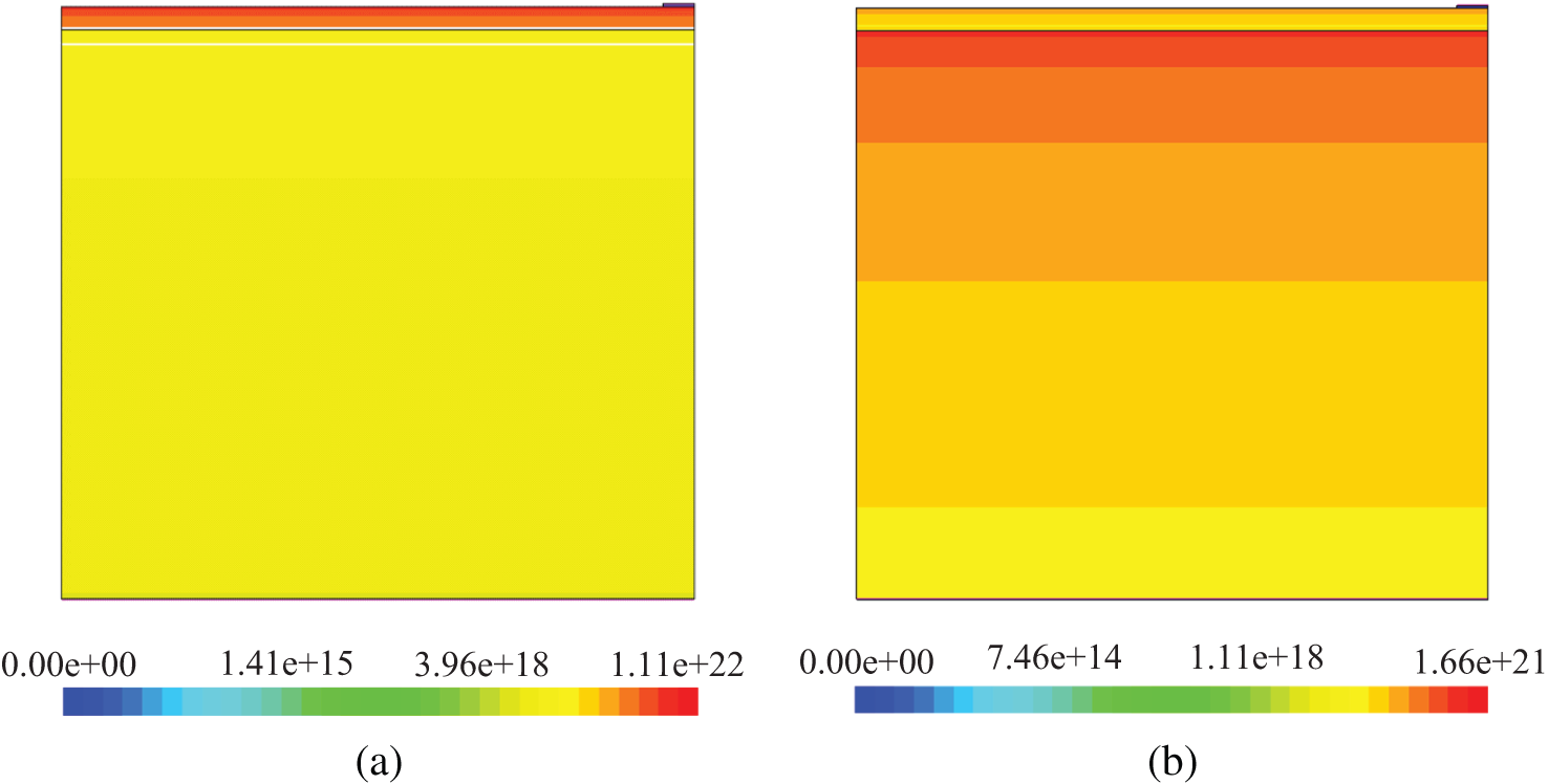
Figure 8: Distribution of absorbed photon density of CH3NH3PbI3/p-Si (a) and n-ZnO/p-Si (b) solar cells. Unit of legend is cm−3
It is emphasized that finding ways to produce new silicon-based heterojunction solar cells without abandoning the traditional silicon-based solar cell manufacturing process is one of today’s key challenges. Therefore, we analyzed and detailed CH3NH3PbI3 and ZnO materials, which can be developed by the Sol-Gel method and formed easily n-type semiconductor as emitter layers for p-type silicon-based heterojunction solar cell. We also explored heterojunction solar cells throughout the simulation. In addition, for the first time, a parameter file consisting of reliable experimental results for ZnO is created, CH3NH3PbI3 and a simulation algorithm in Sentaurus TCAD to model solar cells is developed. The results of our simulation showed that the photoelectric parameters of n-CH3NH3PbI3/p-Si and n-ZnO/p-Si solar cells are better than those of traditional n-Si/p-Si solar cell. However, we found the least improvement in the fill factor of n-ZnO/p-Si, and the best improvement in the fill factor of CH3NH3PbI3. Additionally, we found that the p-n heterojunction of CH3NH3PbI3 with Si is better than that of ZnO with silicon. Moreover, we analyzed the photoelectric parameters of n-CH3NH3PbI3/p-Si and n-ZnO/p-Si solar cells for different thicknesses of the emitter layer. In the interval between 20 and 200 nm, the optimum was located at 80 nm. At which, even the waves generated in the absorption spectrum of ZnO coated silicon solar cell were lost. The results were analyzed using optic parameters for physical justification. We found that CH3NH3PbI3 is a good absorber layer and ZnO is an optimal antireflection coating for silicon-based heterojunction solar cell. In conclusion, it is possible to improve the absorption spectrum of silicon solar cell and increase its efficiency by forming a p-n heterojunction on the basis of a p-type silicon wafer. It is important to note that the materials selected as emitter layer for silicon solar cell should form a good heterojunction with silicon and should have optimal optical properties.
Funding Statement: This work is supported by Fundamental Research Project of Uzbekistan (FZ-2020092973).
Conflicts of Interest: The authors declare that they have no conflicts of interest to report regarding the present study.
References
1. A. Jäger-Waldau, “Snapshot of photovoltaics—February 2019,” Energies 2019, vol. 12, no. 5, pp. 769, 2019. [Google Scholar]
2. S. Rühle, “Tabulated values of the shockley–Queisser limit for single junction solar cells,” Solar Energy, vol. 130, pp. 139–147, 2016. [Google Scholar]
3. J. Gulomov and R. Aliev, “Numerical analysis of the effect of illumination intensity on photoelectric parameters of the silicon solar cell with various metal nanoparticles,” Nanosystems: Physics, Chemistry, Mathematics, vol. 12, no. 5, pp. 569–574, 2021. [Google Scholar]
4. A. Belghachi, “Detailed analysis of surface recombination in crystalline silicon solar cells,” in Proc. of 2013 Int. Renewable and Sustainable Energy Conf., IRSEC 2013, Ouarzazate, Morocco, pp. 161–166, 2013. [Google Scholar]
5. Y. Gassenbauer, K. Ramspeck, B. Bethmann, K. Dressler, J. D. Moschner et al., “Rear-surface passivation technology for crystalline silicon solar cells: A versatile process for mass production,” IEEE Journal of Photovoltaics, vol. 3, no. 1, pp. 125–130, 2013. [Google Scholar]
6. M. S. Sarker, M. F. Khatun, S. R. al Ahmed and J. Hossain, “Optimization of multilayer antireflection coatings for improving performance of silicon solar cells,” in 5th Int. Conf. on Computer, Communication, Chemical, Materials and Electronic Engineering, IC4ME2 2019, Rajshahi, Bangladesh, 2019. [Google Scholar]
7. J. Gulomov and R. Aliev, “Analyzing periodical textured silicon solar cells by the TCAD modeling,” Scientific and Technical Journal of Information Technologies, Mechanics and Optics, vol. 21, no. 5, pp. 626–632, 2021. [Google Scholar]
8. R. Saive, “Light trapping in thin silicon solar cells: A review on fundamentals and technologies,” Progress in Photovoltaics: Research and Applications, vol. 29, no. 10, pp. 1125–1137, 2021. [Google Scholar]
9. A. Shalav, B. S. Richards and M. A. Green, “Luminescent layers for enhanced silicon solar cell performance: Up-conversion,” Solar Energy Materials and Solar Cells, vol. 91, no. 9, pp. 829–842, 2007. [Google Scholar]
10. W. Chen and C. Hong, “Nano-array solid electrode design for photoelectrochemical solar cells,” Computers, Materials & Continua, vol. 21, no. 2, pp. 147–170, 2011. [Google Scholar]
11. J. Gulomov and R. Aliev, “The way of the increasing two times the efficiency of silicon solar cell,” Physics and Chemistry of Solid State, vol. 22, no. 4, pp. 756–760, 2021. [Google Scholar]
12. L. K. Ono and Y. Qi, “Research progress on organic–inorganic halide perovskite materials and solar cells,” Journal of Physics D: Applied Physics, vol. 51, no. 9, pp. 093001, 2018. [Google Scholar]
13. M. Bukleski, S. Dimitrovska-Lazova and S. Aleksovska, “Temperature dependent phase transitions and their relation to isosbestic point formation. Case study of C(NH2)3PBI3,” Spectrochimica Acta Part A: Molecular and Biomolecular Spectroscopy, vol. 266, pp. 120462, 2022. [Google Scholar]
14. L. M. Pazos-Outón, T. P. Xiao and E. Yablonovitch, “Fundamental efficiency limit of lead iodide perovskite solar cells,” Journal of Physical Chemistry Letters, vol. 9, no. 7, pp. 1703–1711, 2018. [Google Scholar]
15. W. E. I. Sha, X. Ren, L. Chen and W. C. H. Choy, “The efficiency limit of CH3NH3PbI3 perovskite solar cells,” Applied Physics Letters, vol. 106, no. 22, pp. 221104, 2015. [Google Scholar]
16. M. Filipic, P. Löper, B. Niesen, S. De Wolf, J. Krč et al., “CH3NH3PbI3 perovskite/silicon tandem solar cells: Characterization based optical simulations,” Optics Express, vol. 23, no. 7, pp. A263–A278, 2015. [Google Scholar]
17. E. Köhnen, P. Wagner, F. Lang, A. Cruz, B. Li et al., “27.9% efficient monolithic perovskite/silicon tandem solar cells on industry compatible bottom cells,” Solar RRL, vol. 5, no. 7, pp. 2100244, 2021. [Google Scholar]
18. J. Wang, Y. Liu, X. Chen, C. Chen, P. Chen et al., “Functional metal oxides in perovskite solar cells,” ChemPhysChem, vol. 20, no. 20, pp. 2580–2586, 2019. [Google Scholar]
19. S. Kerli and Ü. Alver, “Preparation and characterisation of ZnO/NiO nanocomposite particles for solar cell applications,” Journal of Nanotechnology, vol. 2016, 2016. [Google Scholar]
20. K. Sopian, S. L. Cheow and S. H. Zaidi, “An overview of crystalline silicon solar cell technology: Past, present, and future,” AIP Conference Proceedings, vol. 1877, no. 1, pp. 020004, 2017. [Google Scholar]
21. J. Gulomov and R. Aliev, “Influence of the angle of incident light on the performance of textured silicon solar cells,” Journal of Nano-and Electronic Physics, vol. 13, no. 6, pp. 06036–1–06036–5, 2021. [Google Scholar]
22. Y. L. Song, T. J. Zhang, H. J. Du, P. F. Ji, Y. Li et al., “Synthesis, structures and temperature-dependent photoluminescence from ZnO nano/micro-rods on Zn foil,” Materials Letters, vol. 176, pp. 139–142, 2016. [Google Scholar]
23. E. Sermuksnis, M. Ramonas, J. Liberis, A. Matulionis, V. Avrutin et al., “Electron energy relaxation in wurtzite ZnO and GaN,” in 2013 22nd Int. Conf. on Noise and Fluctuations, ICNF 2013, Montpellier, France, 2013. [Google Scholar]
24. D. C. Altamirano-Juarez, R. Castanedo-Perez, O. Jimenez-Sandoval, S. Jimenez-Sandoval, J. Marquez-Marin et al., “Properties of ZnO:AL thin films, bbtained by the Sol-gel method,” MPLB, vol. 15, no. 17–19, pp. 730–732, 2001. [Google Scholar]
25. A. Janotti and C. G. van de Walle, “Fundamentals of zinc oxide as a semiconductor,” Reports on Progress in Physics, vol. 72, no. 12, pp. 126501, 2009. [Google Scholar]
26. H. Ennaceri, A. Taleb, M. Boujnah, A. Khaldoun, J. Ebothé et al., “Theoretical and experimental studies of Al-doped ZnO thin films: Optical and structural properties,” Journal of Computational Electronics, vol. 20, no. 5, pp. 1948–1958, 2021. [Google Scholar]
27. H. J. Xiang, J. Yang, J. G. Hou and Q. Zhu, “Piezoelectricity in ZnO nanowires: A first-principles study,” Applied Physics Letters, vol. 89, no. 22, pp. 223111, 2006. [Google Scholar]
28. R. E. Treharne, A. Seymour-Pierce, K. Durose, K. Hutchings, S. Roncallo et al., “Optical design and fabrication of fully sputtered CdTe/CdS solar cells,” Journal of Physics: Conference Series, vol. 286, no. 1, pp. 012038, 2011. [Google Scholar]
29. Y. Kawamura, H. Mashiyama and K. Hasebe, “Structural study on cubic-tetragonal transition of CH3NH3PbI3,” Journal of the Physical Society of Japan, vol. 71, no. 7, pp. 1694–1697, 2002. [Google Scholar]
30. T. Dittrich, C. Awino, P. Prajongtat, B. Rech and M. C. Lux-Steiner, “Temperature dependence of the band gap of CH3NH3PbI3 stabilized with PMMA: A modulated surface photovoltage study,” Journal of Physical Chemistry C, vol. 119, no. 42, pp. 23968–23972, 2015. [Google Scholar]
31. G. Landi, H. C. Neitzert, C. Barone, C. Mauro, F. Lang et al., “Correlation between electronic defect states distribution and device performance of perovskite solar cells,” Advanced Science, vol. 4, no. 10, pp. 1700183, 2017. [Google Scholar]
32. J. H. Yang, W. J. Yin, J. S. Park and S. H. Wei, “Fast self-diffusion of ions in CH3NH3PbI3: The interstitially mechanism versus vacancy-assisted mechanism,” Journal of Materials Chemistry A, vol. 4, no. 34, pp. 13105–13112, 2016. [Google Scholar]
33. W. Zhao, H. Jiang, B. Liu, J. Song, Y. Jiang et al., “Dielectric huygens’ metasurface for high-efficiency hologram operating in transmission mode,” Scientific Reports 2016 6:1, vol. 6, no. 1, pp. 1–7, 2016. [Google Scholar]
34. F. Staub, U. Rau and T. Kirchartz, “Statistics of the auger recombination of electrons and holes via defect levels in the band gap—Application to lead-halide perovskites,” ACS Omega, vol. 3, no. 7, pp. 8009–8016, 2018. [Google Scholar]
35. C. Chang and C. Liu, “A new optimal iterative algorithm for solving nonlinear poisson problems in heat diffusion,” Computers, Materials & Continua, vol. 34, no. 2, pp. 143–175, 2013. [Google Scholar]
36. Y. Yang, R. A. Nawrocki, R. M. Voyles and H. H. Zhang, “A fractional drift diffusion model for organic semiconductor devices,” Computers, Materials & Continua, vol. 69, no. 1, pp. 237–266, 2021. [Google Scholar]
37. A. T. Hoang, X. P. Nguyen, O. I. Khalaf, T. X. Tran, M. Q. Chau et al., “Thermodynamic simulation on the change in phase for carburizing process,” Computers, Materials & Continua, vol. 68, no. 1, pp. 1129–1145, 2021. [Google Scholar]
38. Y. Xiao, X. Han and D. Hu, “A coupling algorithm of finite element method and smoothed particle hydrodynamics for impact computations,” Computers, Materials & Continua, vol. 23, no. 1, pp. 9–34, 2011. [Google Scholar]
39. W. Xu, G. Yang, P. Lan and H. Ma, “Excluded volumes of anisotropic convex particles in heterogeneous media: Theoretical and numerical studies,” Computers, Materials & Continua, vol. 52, no. 1, pp. 25–40, 2016. [Google Scholar]
40. C. W. J. Beenakker and H. van Houten, “Billiard model of a ballistic multiprobe conductor,” Physical Review Letters, vol. 63, no. 17, pp. 1857, 1989. [Google Scholar]
41. B. Hussain, A. Ali, V. Unsur and A. Ebong, “On structural and electrical characterization of n-ZnO/p-si single heterojunction solar cell,” in Conf. Record of the IEEE Photovoltaic Specialists Conf., Portland, OR, USA, vol. 2016-November, pp. 1898–1901, 2016. [Google Scholar]
42. D. Mukhamedshina, K. Mit’, N. Chuchvaga and N. Tokmoldin, “Fabrication and study of sol-gel ZnO films for use in Si-based heterojunction photovoltaic devices,” Modern Electronic Materials, vol. 3, no. 4, pp. 158–161, 2017. [Google Scholar]
43. X. Rong, H. Tian, W. Bi, H. Jin, T. Zhang et al., “Impact of metal electrode work function of CH3NH3PbI3/p-si planar heterojunction perovskite solar cells,” Solar Energy, vol. 158, pp. 424–431, 2017. [Google Scholar]
44. J. Madan, S. Garg, K. Gupta, S. Rana, A. Manocha et al., “Numerical simulation of charge transport layer free perovskite solar cell using metal work function shifted contacts,” Optik, vol. 202, pp. 163646, 2020. [Google Scholar]
45. S. H. Baek, H. J. Lee and S. N. Lee, “Thickness dependence of crystal and optical characterization on ZnO thin film grown by atomic layer deposition,” AIP Advances, vol. 8, no. 6, pp. 065306, 2018. [Google Scholar]
46. S. S. Shariffudin, M. Salina, S. H. Herman and M. Rusop, “Effect of film thickness on structural, electrical, and optical properties of Sol-gel deposited layer-by-layer ZnO nanoparticles,” Transactions on Electrical and Electronic Materials, vol. 13, no. 2, pp. 102–105, 2012. [Google Scholar]
47. M. R. Rahman, M. N. Uddin, T. Ashrafy, M. Washif, M. R. Uddin et al., “Tuning of optical band gap: Genesis of thickness regulated Al doped ZnO nano-crystalline thin films formulated by Sol–Gel spin coating approach,” Transactions on Electrical and Electronic Materials, vol. 1, pp. 1–14, 2021. [Google Scholar]
48. D. Kanematsu, S. Yoshiba, M. Hirai, A. Terakawa, M. Tanaka et al., “Observation of quantum size effect from silicon nanowall,” Nanoscale Research Letters, vol. 11, no. 1, pp. 1–5, 2016, https://doi.org/10.1186/S11671-016-1743-8. [Google Scholar]
49. H. ElAnzeery, O. E. Daif, M. Buffière, S. Oueslati, K. B. Messaoud et al., “Refractive index extraction and thickness optimization of cu2znsnse4 thin film solar cells,” Physica Status Solidi (a), vol. 212, no. 9, pp. 1984–1990, 2015. [Google Scholar]
50. M. A. Green, “Self-consistent optical parameters of intrinsic silicon at 300 K including temperature coefficients,” Solar Energy Materials and Solar Cells, vol. 92, no. 11, pp. 1305–1310, 2008. [Google Scholar]
51. A. F. Palmstrom, J. Häusele, K. A. Bush, A. F. Palmstrom, J. Carpenter et al., “Optical modeling of wide-bandgap perovskite and perovskite/silicon tandem solar cells using complex refractive indices for arbitrary-bandgap perovskite absorbers,” Optics Express, Vol. 26, vol. 26, no. 21, pp. 27441–27460, 2018. [Google Scholar]
52. A. el Amrani, A. Bekhtari, A. el Kechai, H. Menari, L. Mahiou et al., “Determination of the suitable refractive index of solar cells silicon nitride,” Superlattices and Microstructures, vol. 73, pp. 224–231, 2014. [Google Scholar]
53. E. Chanta, D. Wongratanaphisan, A. Gardchareon, S. Phadungdhitidhada, P. Ruankham et al., “Effect of ZnO double layer as anti-reflection coating layer in ZnO dye-sensitized solar cells,” Energy Procedia, vol. 79, pp. 879–884, 2015. [Google Scholar]
Cite This Article
 Copyright © 2023 The Author(s). Published by Tech Science Press.
This work is licensed under a Creative Commons Attribution 4.0 International License , which permits unrestricted use, distribution, and reproduction in any medium, provided the original work is properly cited.
 Downloads
 Citation Tools