
 Submit a Paper
 Propose a Special lssue
 Open Access
ARTICLE

High-Bandwidth, Low-Power CMOS Transistor Based CAB for Field Programmable Analog Array
1 Advanced Communication Engineering (ACE), Centre of Excellence, Universiti Malaysia Perlis (UniMAP), Faculty of Electronic Engineering Technology, Kangar, 01000, Malaysia
2 Electrical Engineering, King Fahd University of Petroleum and Minerals, Dhahran, Eastern, 31261, Saudi Arabia
3 Space Science Centre, Climate Change Institute, Universiti Kebangsaan Malaysia, Bangi, 43600, Malaysia
4 Department of Electronics & Communication Engineering, Faculty of Engineering & Petroleum, Hadhramout University, Al-Mukalla, Hadhramout, 50512, Yemen
5 Faculty of Engineering, Norwegian University of Science and Technology (NTNU), Gjøvik, N-2815, Norway
6 Faculty of Electronic Engineering Technology, Universiti Malaysia Perlis (UniMAP), Kampus Alam UniMAP Pauh Putra, Arau, 02600, Malaysia
7 Department of General Educational Development, Faculty of Science and Information Technology (FSIT), Daffodil International University, Dhaka, 1207, Bangladesh
8 Department of Electronics and Computer Engineering (FKEKK), Center for Telecommunication Research and Innovation (CeTRI), Universiti Teknikal Malaysia Melaka (UTeM), Durian Tungal, 76100, Malaysia
9 Department of Electrical Engineering, University of Sharjah, Sharjah, 27272, United Arab Emirates
* Corresponding Author: Samir Salem Al-Bawri. Email:
Computers, Materials & Continua 2023, 74(3), 5885-5900. https://doi.org/10.32604/cmc.2023.033789
Received 27 June 2022; Accepted 15 September 2022; Issue published 28 December 2022
 View Full Text
 Download PDF
Abstract
This article presents an integrated current mode configurable analog block (CAB) system for field-programmable analog array (FPAA). The proposed architecture is based on the complementary metal-oxide semiconductor (CMOS) transistor level design where MOSFET transistors operating in the saturation region are adopted. The proposed CAB architecture is designed to implement six of the widely used current mode operations in analog processing systems: addition, subtraction, integration, multiplication, division, and pass operation. The functionality of the proposed CAB is demonstrated through these six operations, where each operation is chosen based on the user’s selection in the CAB interface system. The architecture of the CAB system proposes an optimized way of designing and integrating only three functional cells with the interface circuitry to achieve the six operations. Furthermore, optimized programming and digital tuning circuitry are implemented in the architecture to control and interface with the functional cells. Moreover, these designed programming and tuning circuitries play an essential role in optimizing the performance of the proposed design. Simulation of the proposed CMOS Transistor Based CAB system is carried out using Tanner EDA Tools in 0.35 μm standard CMOS technology. The design uses a V power supply and results in maximum 3 dB bandwidth of 34.9 MHz and an approximate size of 0.0537 . This demonstrates the advantages of the design over the current state-of-the-art designs presented for comparison in this article. Consequently, the proposed design has a clear aspect of simplicity, low power consumption, and high bandwidth operation, which makes it a suitable candidate for mobile telecommunications applications.Keywords
Since the early 1990s of the previous century, researchers have begun to develop numerous designs of the analog equivalent of the field-programmable gate array (FPGA), which is the field-programmable analog array (FPAA) [1]. Analog solutions are becoming increasingly competitive with digital circuits, particularly for compact, low-power, and high-speed applications [2]. This is despite the fact that digital processing circuits currently hold the majority of the market share. This is because analog circuits are capable of performing essential signal processing activities quicker than their digital counterparts while also consuming less power and occupying a smaller area of silicon. The true value of FPAA design comes from its application in the prototyping, testing, and development of analog circuits. Because of its reconfigurable architecture, which enables rapid and low-cost prototyping, the FPAA would be an excellent tool for testing and prototyping analog circuitry design [2]. In addition, the use of analog circuits would be made accessible to designers who do not have extensive expertise in the relevant subject, capitalizing on the FPAAs features. Therefore, the trend toward shorter design cycles and cheaper prices for analog integrated circuits has required the creation of various advances in the area of FPAA and related configurable analog blocks (CABs) [3]. These advancements have been necessary because of the nature of the field itself and the need to reach a commonly used widely acceptable CAB Structure.
There has been recent interest by researchers in the area of FPAA and the design of its core element, which is the CAB. Many publications in the literature used active elements such as operational amplifier (Op-amp), operational transconductance amplifier (OTA), second-generation current conveyors (CCII), or current feedback operational amplifier (CFOA) in the design of CAB [4–8]. At this time, the vast majority of the FPAAs that are available (commercially and academically) are often based on CABs that involve operational amplifiers or other analog primitives with a similar function [9–11]. Because these designs are dependent on the active elements, the resulting CAB performance was restricted according to the capabilities of the elements themselves. In addition, some designs do not contain any active components; rather, these designs are built at the transistor level [1,12]. The transistor level design CAB can be accomplished with metal–oxide–semiconductor field-effect transistor (MOSFET) sub-threshold as described in [13], with BJT transistors as presented in [14], or with a multi trans-linear element (MITE) and Floating gate transistors (FG) as shown in [1,15]. Because of this, numerous CAB designs have been developed. These designs are at the core of the FPAA systems. The transistor level-based approach and other similar approaches were also the basis of the designs presented in [13,14,16].
The following Table 1 summarizes some of the designs in the literature and provides a comparative analysis of the approach adopted in each design and other important design features.

1.2 Research Gap and Contribution
As highlighted earlier, the vast majority of available CAB designs incorporate an active element(s) as the basis of the design structure. Consequently, the designed CABs can only perform to the capabilities limits of the individual active element(s). Therefore, this article presents a design for a configurable analog block system based on the transistor-level design technique of MOSFETs operating in strong inversion. As a result, the highlighted limitations of using active primitive elements in the CAB are avoided, which opens the potential for numerous advancements in the CAB design. Furthermore, minimal research has been carried out in this field using a transistor-level design approach; hence, we took strides to contribute to this field. Even though few designs exist based on similar approaches, our proposed work innovatively incorporates several enhanced features in an optimized way.
The ever-presented demand for high-frequency operation and lower supply voltages are among the main requirements that affect the design of the CABs of any FPAA [17]. As highlighted throughout this paper, the overall findings showed improved performance regarding the amount of power consumed and the bandwidth available based on our adopted method. Due to the system’s integrated interface circuitry of the proposed design, it only utilizes three functional cells to perform addition/subtraction/pass, integration, and multiplication/division based on the user’s selection. Apart from that, the outcome from the system suggested that the programming of the functions and parameters should primarily be accomplished by modifying the bias condition of the circuits, in addition to the limited use of three switches. Moreover, the use of limited switches is partially regarded for the bandwidth optimization.
The main contribution of this work is summarized in the following points:
• Design of a new optimized CAB structure at the transistor level with advanced features of high bandwidth, low power consumption, and a relatively small area for potential use as the main block in FPAA design.
• Design of a current mode functional cell at the transistor level to perform addition, subtraction, and pass functions with all programming, tuning, and interfacing circuitry needed.
• Design of a current model functional cell at the transistor level to perform integration function through optimizing an inverter lossless integrator and designing all programming, tuning, and interfacing circuitry needed.
• Design of a current model functional cell at the transistor level to perform multiplication and division functions through optimizing a current mode multiplier and designing all programming, tuning, and interfacing circuitry needed.
• Design of all interconnections and switches needed for the overall integration.
• Optimized Integration of the three design functional cells for advanced performance in bandwidth, power consumption, and area occupation.
The rest of this paper is organized as follows (2) Proposed Design (3) Results and Discussion (4) Conclusion.
The CAB system circuitry is integrated and structured uniquely to make reconfigurability possible and to reduce power consumption for the unused parts of the design during certain operations. Fig. 1 depicts the proposed design, which consists mainly of the three functional cells connected in series where each is capable of processing certain functions on the input signals. The “adder, subtractor, pass” cell is the first cell in the circuit, and it is the one into which the input is initially inserted. The output of this cell is connected to the subsequent cell, which is an integrator cell. Within this cell, the signal can either be integrated or simply bypassed through a switch and sent on to the subsequent cell. The multiplier/divider cell is represented by the third cell in Fig. 1. The current mirrors at the output are connected to the multiplier/divider cell’s output to complete the circuit. Since the three cells make up the CAB, this architecture makes it possible for the CAB to implement a single function, double functions, or even triple functions all at the same time. This is because the CAB is set up in such a way that each cell’s bias currents can be individually controlled, allowing for activation or deactivation of the cell as needed. In addition, the design reduces the amount of power consumption required during the activation and deactivation of the bias currents present in the system.
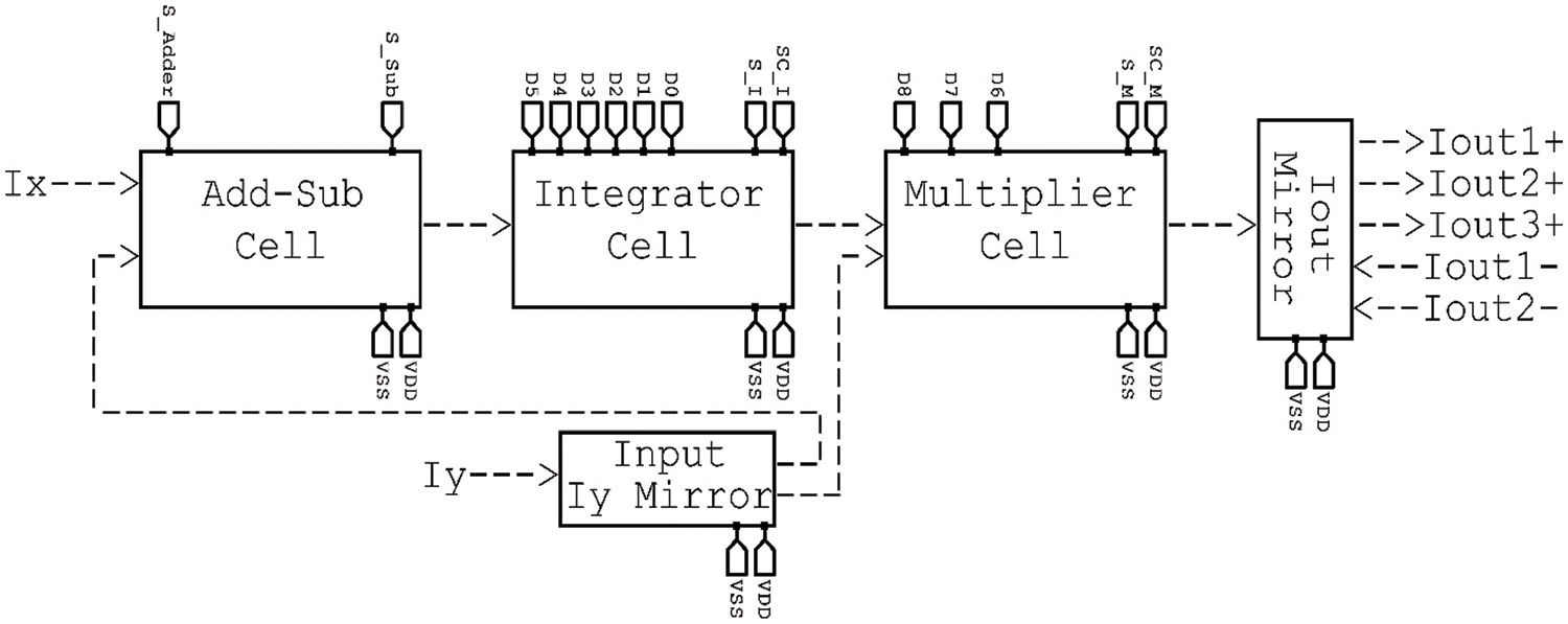
Figure 1: Proposed CAB system design and interfacing
Furthermore, bias current circuits are integrated with each cell to make activation and deactivation possible. Each functional cell was designed and then integrated with its bias currents. The final circuit of each designed cell was then simulated for its intended functionality.
2.1 Adder/Subtractor/Pass Functional Cell
Even though addition and subtraction can be done relatively easily in the current mode, the proposed design avoids using switches in the signal path to ensure optimum performance, as depicted in Fig. 2. The current sources controlled the cell programmability are
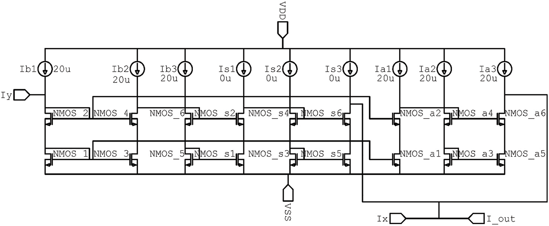
Figure 2: Proposed adder/subtractor/pass functional cell design

In the subtraction case, an inverted copy of
Switchless current mode integrators are highly recommended because the extensive use of switches and capacitors can severely degrade the frequency response of the circuit [18]. Several continuous time current mode integrators have been reported in the literature. One family of such integrators is the current mirrors transconductance capacitance
An integrator that is very much like the one described in [20] and shown in Fig. 3 was utilized here. The integrator in [20] does not make use of starting low-frequency operation. Its starting frequency operation is somewhere around 100 kHz, but for extended use and utilization, it needs to be extended to lower frequencies than that. In addition to this, it cannot be configured, nor can it be programmed. The proposed integrator shown in Fig. 3 gets around these restrictions by considering the values of the bias current to increase the frequency at which it can function. Furthermore, the integrator is made configurable through the manipulation of the bias currents that are used in the circuit. The components of this circuit are a capacitor labeled C 1, two straightforward current mirrors, and biasing currents. The operation of the integrator can be controlled and fine-tuned through the use of programmable current sources, as shown in Fig. 3. However, Fig. 4 depicts the small-signal model of the circuit with the output conductance omitted from consideration based on the mathematical model of low-level signals:
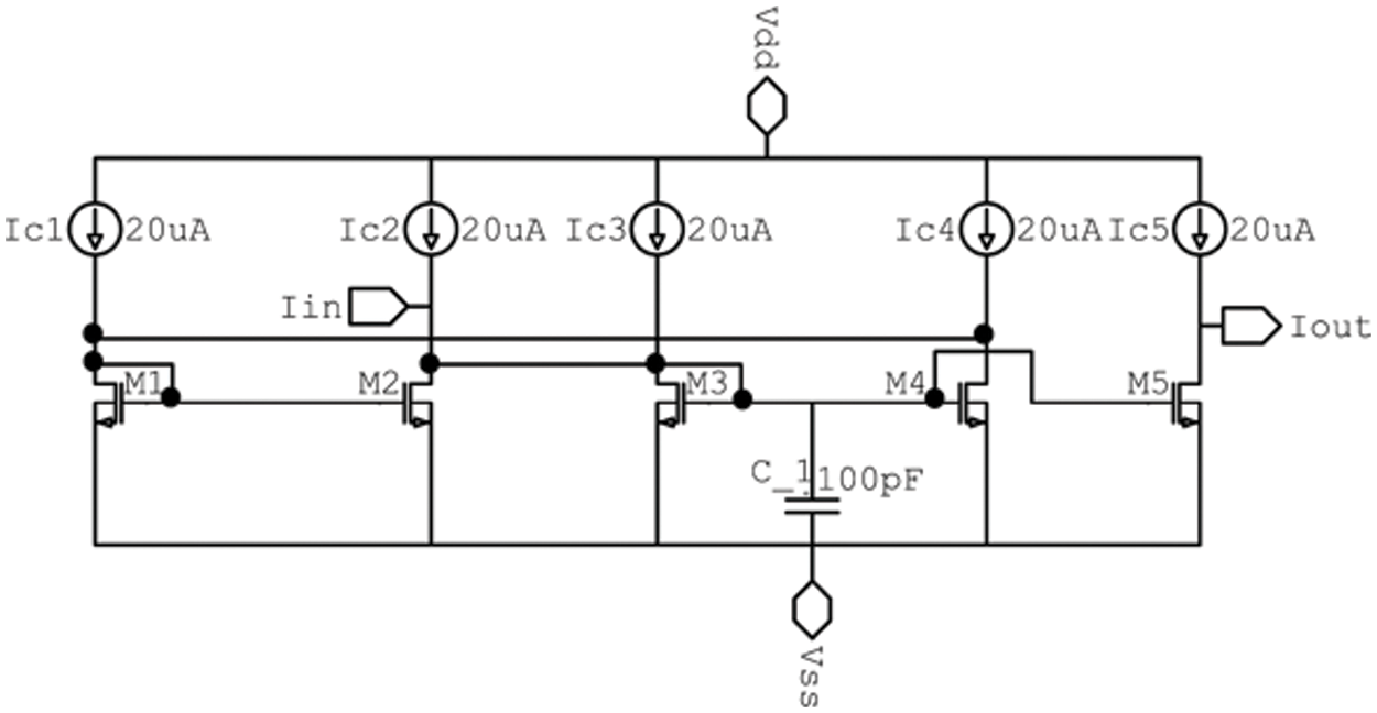
Figure 3: Proposed inverting lossless integrator
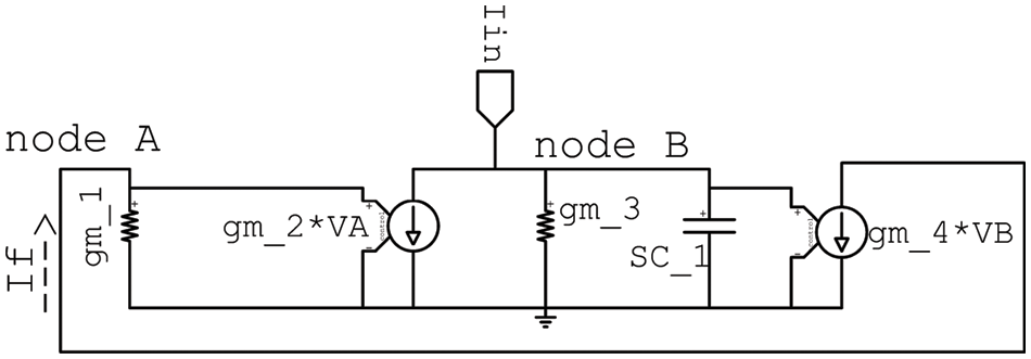
Figure 4: Integrator small signal model
Assuming that
Since
Eq. (6) represents the transfer function of an inverting type lossless integrator. The integrator unity gain frequency is determined by the factor
2.3 Multiplier/Divider Circuit
Multiplier circuits are very fundamental blocks in signal processing systems. This justifies the growing interest in developing this circuit, proven by many publications in this area; see [23–27]. A multiplier/divider circuit is reported in [23]. That circuit is based on dual trans-linear loops of MOSFET transistors operating in saturation. It is reported to achieve a bandwidth of 41.8 MHZ and power consumption of 340 μW. The improved circuit to [23] is in [28] and is designed by the authors of this paper to be used in the CAB design.
Fig. 5 represents the circuit structure of the proposed designed multiplier/divider circuit reported in [28] and proposed to be used here. Its achieved bandwidth has been enhanced to 440 MHz and the reported power consumption is reduced to about 158 μW. The relationship between the input currents (
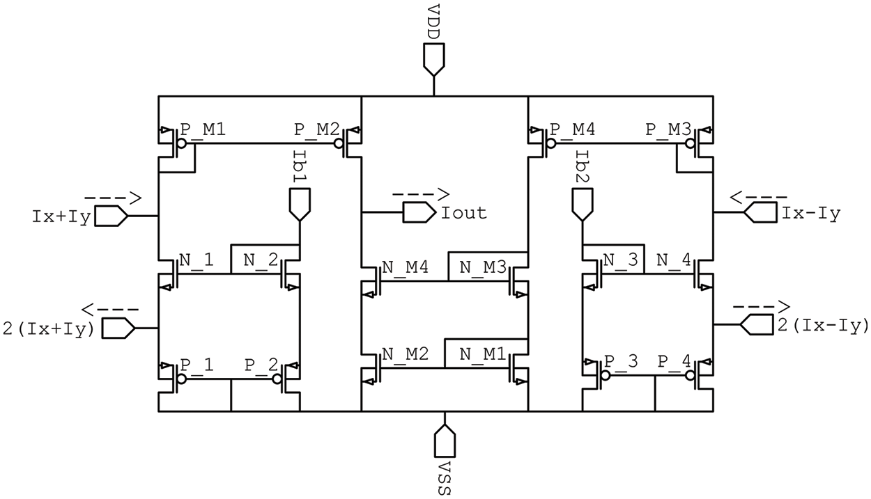
Figure 5: Proposed multiplier/divider circuit designed by the same authors in [28]
From (8), it is obvious that the circuit functions as a multiplication of two signals
2.4 Configurable Biasing Sources, Programmable Tuning, and Interfacing Circuit Design
The designed circuit was used as the configuring tool for the adder/subtractor is presented in Fig. 6a. It can to activate or deactivate the biasing currents. This, in turn, activates or deactivates the complete circuit connected to the biasing currents. This circuit was used to bias the adder-subtractor circuit previously shown in Fig. 2. This circuit generates three equal copies of current
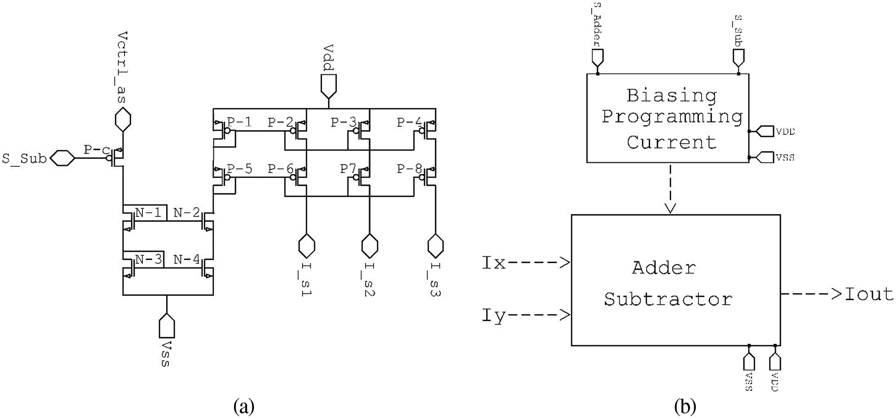
Figure 6: (a) Programming circuit for subtraction cell, (b) complete adder/subtractor configurable cell
To control and tune the parameters of the integrator circuit, programmable tunable currents need to be designed and used in the integrator circuit as part of the configuring tool [18]. The digitally programmable currents circuit in Fig. 7 was used. The tunability in the design was achieved at two levels: coarse tuning and fine tuning. The circuit in Fig. 7 achieves the coarse tuning; The coarse tuning circuit can generate a current ranging from
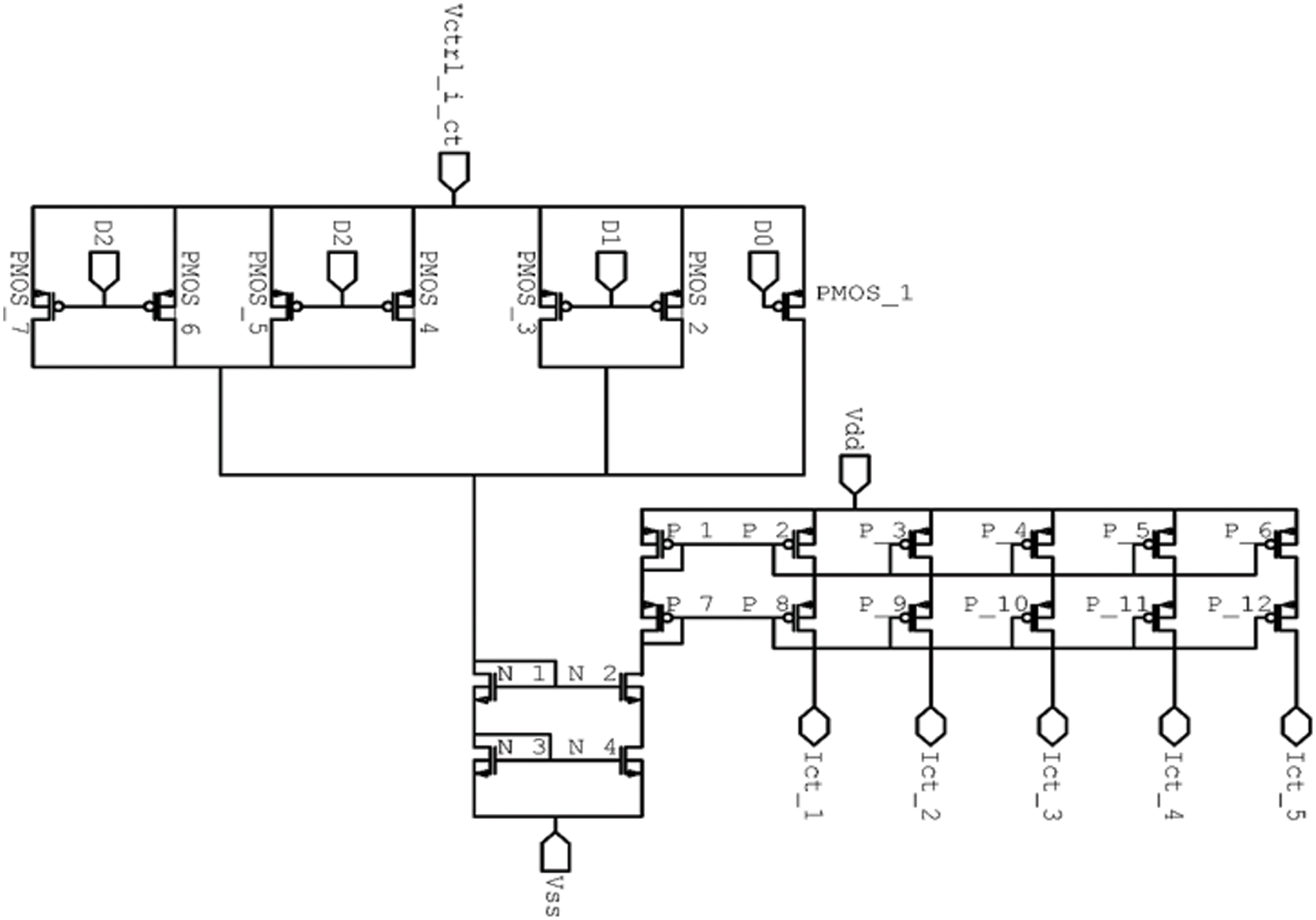
Figure 7: Digitally programmable coarse tuning current for the integrator
Fig. 8 presents the complete integrator programmable and tunable structure. This part of the overall design is programmed and controlled by five bits D_0 to D_5. In addition, limited use of only one switch at the input node is adopted. Furthermore, Fig. 9 shows the complete structure of the multiplier/divider circuit including the current mirrors, biasing and tuning currents, and limited use of two switches at the input and the output of the structure. It can also be noticed that this block can be controlled with three bits D_6 to D_8.
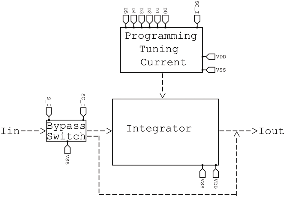
Figure 8: Complete integrator tunable cell
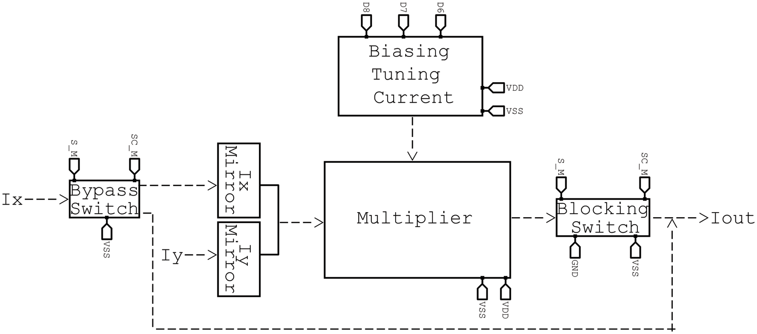
Figure 9: Complete configurable and tunable multiplier/divider cell
The utilization of CMOS transistor switches is included as a component of the design in very limited cases. A bypass switch and a blocking switch are the two kinds of switches that are utilized here. The bypass switch is situated at the integrator’s input and can either allow the input to be incorporated into the circuit or divert it directly to the output of the integrator. Additionally, bypass transistors with the same functionality were utilized at the input (Ix) of the multiplier/divider. The output of the multiplier/divider was where the blocking switch was utilized. It only permits the current to flow in one direction from the output (out of the multiplier).
2.5 Control Word and Overall, CAB Interface
The mode of operation of the CAB can be digitally selected using the bits that are displayed in Table 3, which are part of the control word. According to the preferences of the user, each of these bits in the table is in charge of activating or deactivating a specific part of the system that was designed. At this point, it is possible to ascertain the comprehensive CAB digital control word. It is made up of a total of 13 bits. As can be seen in Fig. 10, it is split into two sections: the part that deals with programming and the part that deals with tuning. Fig. 10 illustrates how the CAB interfaces with the control word.

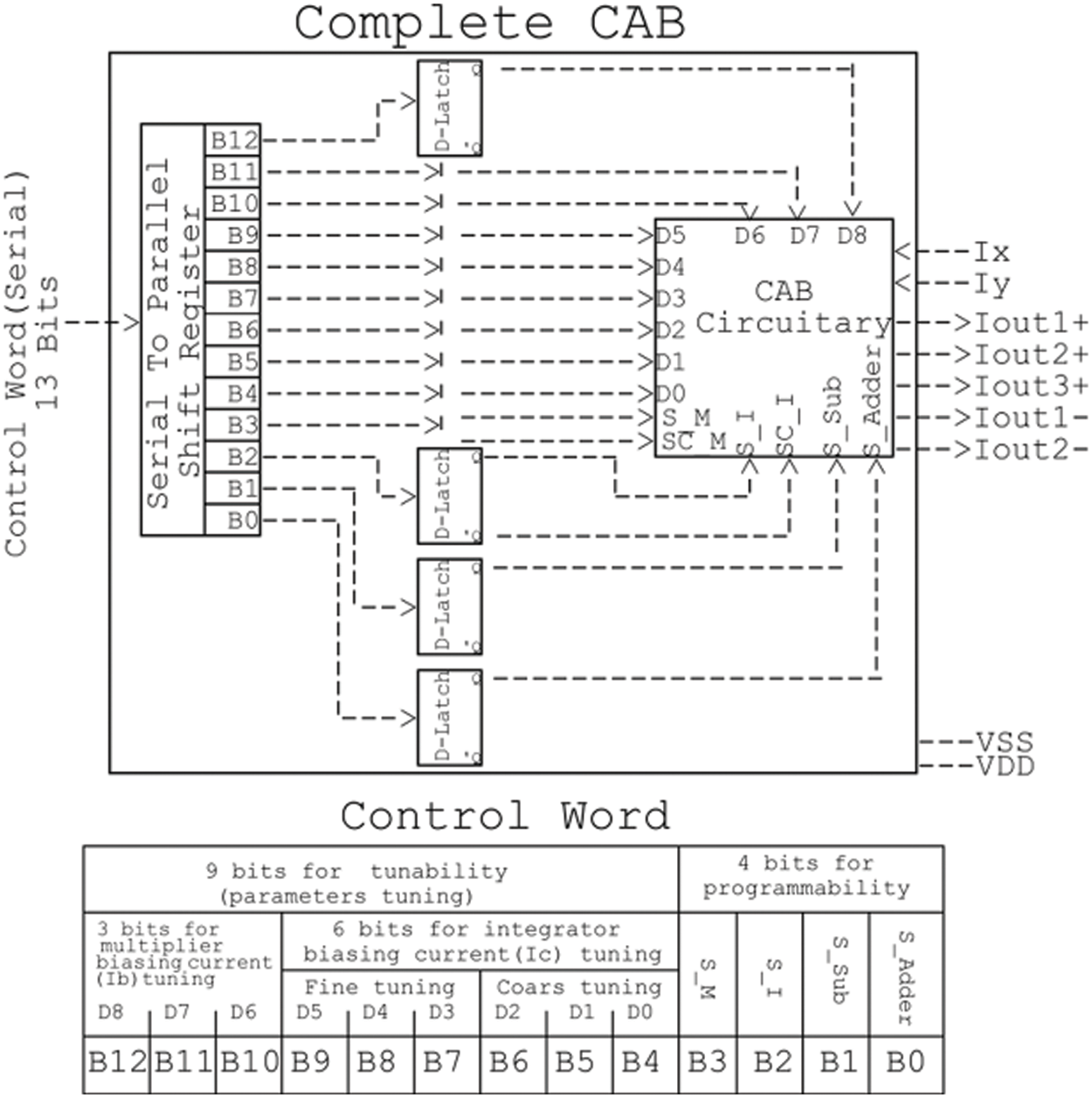
Figure 10: Complete CAB Illustration with the control word
To investigate the performance of the proposed circuits and to prove their functionality, Tanner simulation results are reported in this section using 0.35 μm standard CMOS technology. Simulation results of the circuit in Fig. 2 are obtained at biasing currents = 20 μA or 0 μA,
Fig. 11a shows the transient response of the circuit when the inputs are sinusoidal signals. The input
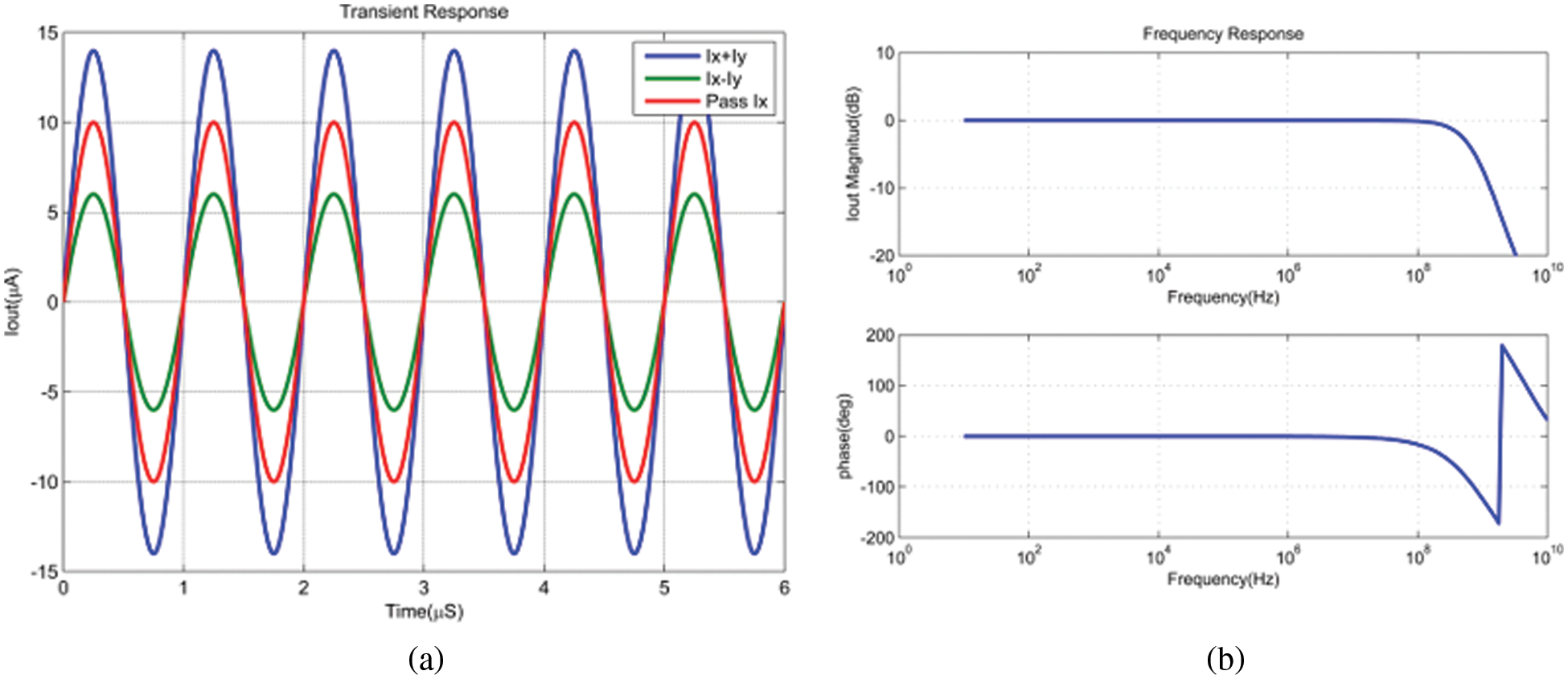
Figure 11: (a) Transient response of the adder-subtractor cell for addition, subtraction, and pass, (b) frequency response of the adder-subtractor cell
Simulation results of the circuit in Fig. 3 are obtained at biasing currents
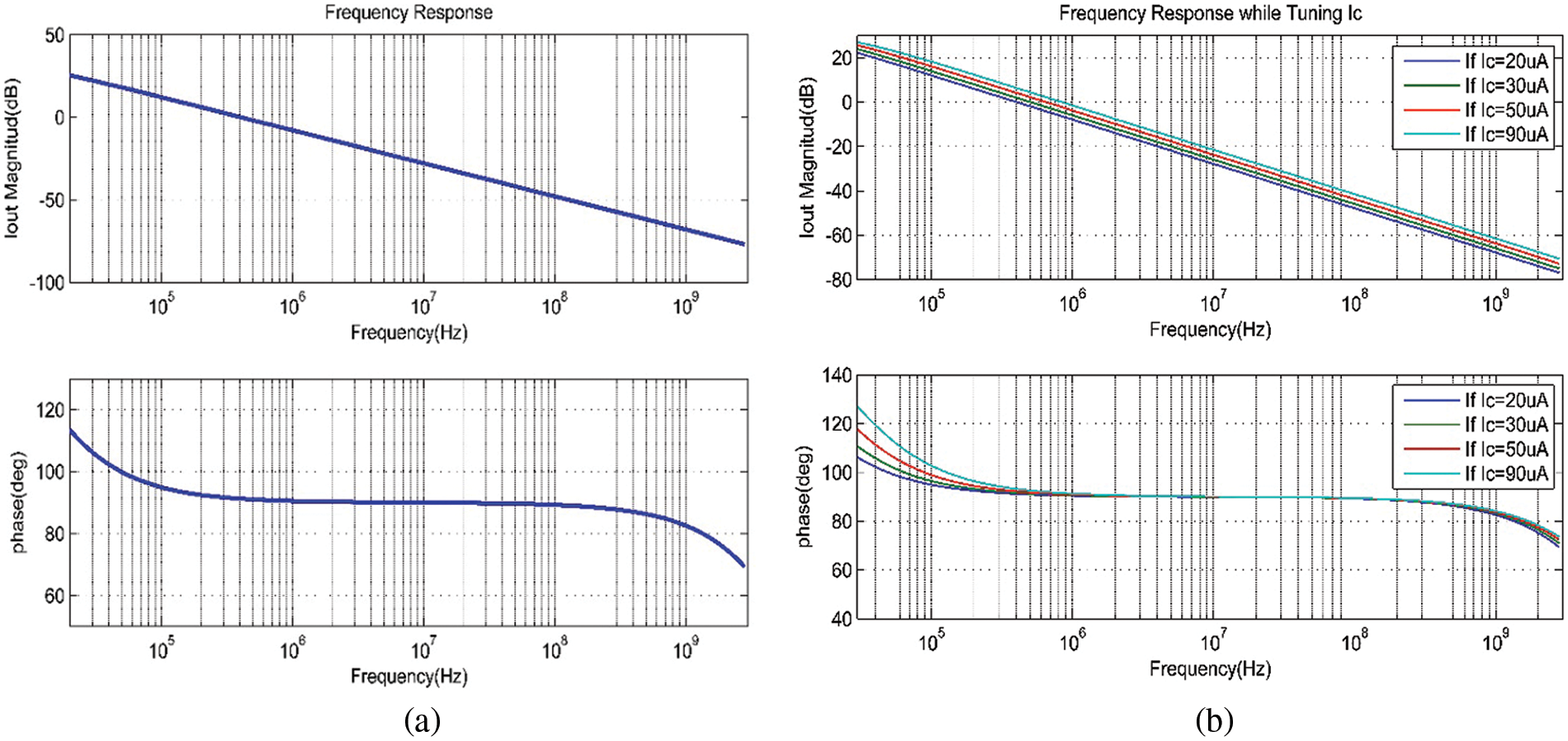
Figure 12: (a) Integrator frequency response, (b) integrator frequency response while tuning Ic
Simulation of the proposed multiplier/divider is carried out based on the following circuit parameters:
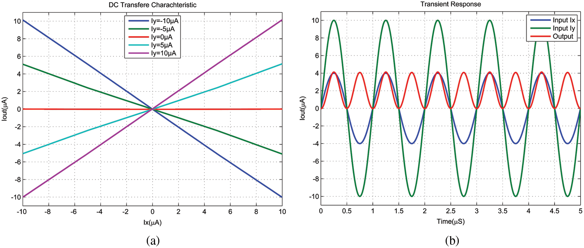
Figure 13: (a) DC transfer characteristic of the proposed multiplier/divider, (b) transient response of the proposed multiplier/divider
The proposed circuit has an error in the linearity of approximately 1.1 percent and has a power consumption of approximately 158 microwatts. The transient response of the multiplier is depicted in Fig. 13b when both inputs (Ix and Iy) are sinusoidal signals operating at a frequency of 1 MHz with two different amplitudes. However, Fig. 14 illustrates the frequency response of the proposed multiplier/divider device. The circuit has a bandwidth of about 440 MHz when measured at a dB level of −3.
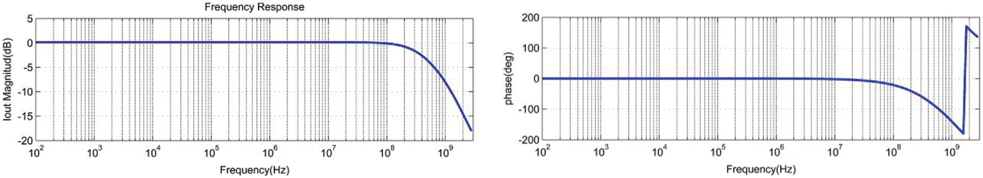
Figure 14: Frequency response of the proposed multiplier/divider
A comparison between the proposed CAB design and previous designs is reported in Table 4. The designs reported in [13,16] are based on the same method adopted in the proposed design. However, the proposed CAB enjoys better features, especially in terms of bandwidth. The design in [14] exhibits better bandwidth than the proposed CAB, however, this is because [14] adopts BJT technology rather than CMOS. Moreover, the introduced design consumes low power, and it is suitable for integration since it uses only MOSFET transistors and a grounded capacitor. To sum up, the main attractive features of this design are small size, simplicity, low power consumption, and high bandwidth. In addition, there is a lack of designs in the literature adopting the method used in this work which gives an advantage to this proposed design. However, one weakness of the design is in that the division function range is very limited. This is because the denominator is the bias current which can be varied only to a limited extent.

Within the scope of this paper, a novel architecture of CAB for FPAA application was presented. The current mode MOSFET transistor level was utilized for this design and was implemented to operate in the saturation region. The proposed CAB structure is capable of performing operations such as addition, subtraction, pass, multiplication, division, and integration based on only three functional cells. Because the functional cells are combined in series, the proposed design is also capable of performing double or triple operations at the same time due to the optimized functional cells. Furthermore, the programming of the CAB is accomplished primarily by adjusting the biasing condition of the circuit with limited use of switches. The proposed structure shows high-performance results when compared to some of the state-of-the-art results. With the use of
Funding Statement: This work was supported in part by the Geran Galakan Penyelidik Muda Grant (GGPM), Universiti Kebangsaan Malaysia, Selangor, Malaysia under grant GGPM-2021-055.
Conflicts of Interest: The authors declare that they have no conflicts of interest to report regarding the present study.
References
1. C. R. Schlottmann, D. Abramson and P. E. Hasler, “A MITE-based translinear FPAA,” IEEE Transactions on Very Large Scale Integration (VLSI) Systems, vol. 20, no. 1, pp. 1–9, 2012. [Google Scholar]
2. D. R. D’Mello and P. G. Gulak, “Design approaches to field-programmable analog integrated circuits,” Analog Integrated Circuits and Signal Processing, vol. 17, no. 1–2, pp. 7–34, 1998. [Google Scholar]
3. H. W. Klein, “The EPAC architecture: An expert cell approach to field programmable analog devices,” in Proc. of the 1996 ACM 4th Int. Symp. on Field-Programmable Gate Arrays, FPGA 1996, Monterey California, USA, pp. 94–99, 1996. [Google Scholar]
4. M. M. Maryan and S. J. Azhari, “Ultra-low-power low-voltage FGMOS based-configurable analog block for current-mode fractional-power functions,” Microelectronics Journal, vol. 64, pp. 99–105, 2017. [Google Scholar]
5. S. Nikseresht and S. J. Azhari, “A new current-mode computational analog block free from the body-effect,” Integration, vol. 65, pp. 18–31, 2019. [Google Scholar]
6. M. S. Diab and S. Mahmoud, “Field programmable analog array for low-frequency application of OTA-C low pass filters,” in 2020 43rd Int. Conf. on Telecommunications and Signal Processing, TSP 2020, Milan, Italy, pp. 685–688, 2020. [Google Scholar]
7. S. Mahmoud and E. Soliman, “Novel CCII-based field programmable analog array and its application to a sixth-order butterworth LPF,” Radioengineering, vol. 22, no. 2, pp. 440–447, 2013. [Google Scholar]
8. H. Alzaher, “Current follower based reconfigurable integrator/differentiator circuits with passive and active components’ reuse,” Microelectronics Journal, vol. 46, no. 2, pp. 135–142, 2015. [Google Scholar]
9. M. S. Diab and S. A. Mahmoud, “On the design of OTA-C based field programmable analog arrays for continuous time low-frequency applications,” Microelectronics Journal, vol. 103, pp. 104870, 2020. [Google Scholar]
10. S. Maheshwari, “Configurable analog block using current-mode approach,” Journal of Circuits, Systems and Computers, vol. 31, no. 2, pp. 2250037, 2022. [Google Scholar]
11. M. S. Diab and S. A. Mahmoud, “Survey on field programmable analog array architectures eliminating routing network,” IEEE Access, vol. 8, pp. 220779–220794, 2020. [Google Scholar]
12. N. Suda, J. Suh, N. Hakim, Y. Cao and B. Bakkaloglu, “A 65 nm programmable analog device array (PANDA) for analog circuit emulation,” IEEE Transactions on Circuits and Systems I: Regular Papers, vol. 63, no. 2, pp. 181–190, 2016. [Google Scholar]
13. S. Sa-ad and D. Chaythong, “A High-frequency current mode ladder filter using multiple output lossless integrator,” in 2008 Int. Symp. on Intelligent Signal Processing and Communication Systems, ISPACS 2008, Bangkok, Thailand, pp. 1–4, 2009. [Google Scholar]
14. A. H. Madian, S. A. Mahmoud and A. M. Soliman, “Field programmable analog array based on CMOS CFOA and its application,” in Proc. of the 15th IEEE Int. Conf. on Electronics, Circuits and Systems, ICECS 2008, Saint Julian’s, Malta, pp. 1042–1046, 2008. [Google Scholar]
15. S. Kim, S. Shah, R. Wunderlich and J. Hasler, “CAD synthesis tools for floating-gate SoC FPAAs,” Design Automation for Embedded Systems, vol. 25, no. 3, pp. 161–176, 2021. [Google Scholar]
16. S. H. K. Embabi, X. Quan, N. Oki, A. Manjrekar and E. Sanchez-Sinencio, “Field programmable analog signal processing array,” in Midwest Symp. on Circuits and Systems, Ames, IA, USA, pp. 151–154, 1996. [Google Scholar]
17. M. S. Diab and S. A. Mahmoud, “Field programmable analog arrays for implementation of generalized nth-order operational transconductance amplifier-C elliptic filters,” In Electronics and Telecommunications Research Institute (ETRI) Journal, vol. 42, no. 4, pp. 534–548, 2020. [Google Scholar]
18. O. Fares, “Configurable analog building blocks for field programmable analog arrays,” Ph.D. dissertation, King Fahd University of Petroleum and Minerals, 2004. [Google Scholar]
19. R. H. Zele and D. J. Allstot, “Low-power CMOS continuous-time filters,” IEEE Journal of Solid-State Circuits, vol. 31, no. 2, pp. 157–168, 1996. [Google Scholar]
20. W. Tangsrirat, “Low-voltage digitally programmable current-mode universal biquadratic filter,” AEÜ-International Journal of Electronics and Communications, vol. 62, no. 2, pp. 97–103, 2008. [Google Scholar]
21. J. Feng, C. Wang, M. Zang and Y. Ren, “Realization of current-mode general nth-order filter based on current mirrors,” in 2011 3rd Int. Conf. on Advanced Computer Control, ICACC 2011, Harbin, China, pp. 367–370, 2011. [Google Scholar]
22. C. Laoudias and C. Psychalinos, “Universal biquad filter topology using low-voltage current mirrors,” International Journal of Circuit Theory and Applications, vol. 40, no. 1, pp. 65–75, 2012. [Google Scholar]
23. A. Naderi, A. Khoei and K. Hadidi, “High speed, low power four-quadrant CMOS current-mode multiplier,” in Proc. of the IEEE Int. Conf. on Electronics, Circuits, and Systems, Marrakech, Morocco, pp. 1308–1311, 2007. [Google Scholar]
24. B. Ghanavati, A. Khoei and K. Hadidi, “± 1.2 V high frequency four quadrant current multiplier,” in ASICON 2007-2007 7th Int. Conf. on ASIC Proc., Guilin, China, pp. 169–172, 2007. [Google Scholar]
25. M. A. Al-Absi, A. Hussein and M. T. Abuelma’atti, “A novel current-mode ultra-low power analog CMOS four quadrant multiplier,” in 2012 Int. Conf. on Computer and Communication Engineering, ICCCE 2012, Kuala Lumpur, Malaysia, pp. 13–17, 2012. [Google Scholar]
26. S. Kaedi and E. Farshidi, “A new low voltage four-quadrant current mode multiplier,” in ICEE 2012-20th Iranian Conf. on Electrical Engineering, Tehran, Iran, pp. 160–164, 2012. [Google Scholar]
27. M. Gravati, M. Valle, G. Ferri, N. Guerrini and L. Reyes, “A novel current-mode very low power analog CMOS four quadrant multiplier,” in Proc. of ESSCIRC 2005: 31st European Solid-State Circuits Conf., Grenoble, France, pp. 495–498, 2005. [Google Scholar]
28. A. Hussein and A. Bin, “Improved high-speed low power CMOS multiplier,” in Third Int. Conf. on Advances in Computing, Electronics and Electrical Technology-CEET 2015, Kuala Lumpur, Malaysia, pp. 64–68, 2015. [Google Scholar]
29. B. Pankiewicz, M. Wojcikowski, S. Szczepanski and Y. Sun, “A CMOS field programmable analog array and its application in continuous-time OTA-C filter design,” in ISCAS 2001-2001 IEEE Int. Symp. on Circuits and Systems, Conf. Proc., Sydney, NSW, Australia, vol. 1, pp. 5–8, 2001. [Google Scholar]
30. E. A. Soliman and S. A. Mahmoud, “Voltage-mode field programmable analog array using second generation current conveyor,” in IEEE 55th Int. Midwest Symp. on Circuits and Systems (MWSCAS), Boise, ID, USA, pp. 710–713, 2012. [Google Scholar]
31. A. H. Madian, S. A. Mahmoud and A. M. Soliman, “New 1.5-V CMOS current feedback operational amplifier,” in Proc. of the IEEE Int. Conf. on Electronics, Circuits, and Systems, Nice, France, pp. 600–603, 2006. [Google Scholar]
32. K. Maheshwari, S. Maheshwari and P. Yadav, “Design of configurable analog block-based oscillator and possible applications,” In Lecture Notes in Networks and Systems, vol. 106, pp. 621–630, 2020. [Google Scholar]
33. X. Quan, S. H. K. Embabi and E. Sanchez-Sinencio, “Current-mode based field programmable analog array architecture for signal processing applications,” in Proc. of the Custom Integrated Circuits Conf., Santa Clara, CA, USA, pp. 277–280, 1998. [Google Scholar]
34. M. T. Abuelma’atti and O. O. Fares, “A new universal second-order filter using configurable analog building blocks (CABs) for filed-programmable analog arrays,” Journal of Engineering Research (JER), vol. 8, no. 1, pp. 83–91, 2011. [Google Scholar]
Cite This Article
 Copyright © 2023 The Author(s). Published by Tech Science Press.
This work is licensed under a Creative Commons Attribution 4.0 International License , which permits unrestricted use, distribution, and reproduction in any medium, provided the original work is properly cited.
 Downloads
 Citation Tools