
 Submit a Paper
 Propose a Special lssue
 Open Access
ARTICLE

A Low-Power 12-Bit SAR ADC for Analog Convolutional Kernel of Mixed-Signal CNN Accelerator
1 Department of Electronics, College of Electrical and Computer Engineering, Chungbuk National University, Cheongju, 28644, Korea
2 Department of Electrical and Computer Engineering, COMSATS University Islamabad, Abbottabad Campus, University Road, Tobe Camp, Abbottabad, 22044, Pakistan
* Corresponding Author: HyungWon Kim. Email:
Computers, Materials & Continua 2023, 75(2), 4357-4375. https://doi.org/10.32604/cmc.2023.031372
Received 15 April 2022; Accepted 30 January 2023; Issue published 31 March 2023
 View Full Text
 Download PDF
Abstract
As deep learning techniques such as Convolutional Neural Networks (CNNs) are widely adopted, the complexity of CNNs is rapidly increasing due to the growing demand for CNN accelerator system-on-chip (SoC). Although conventional CNN accelerators can reduce the computational time of learning and inference tasks, they tend to occupy large chip areas due to many multiply-and-accumulate (MAC) operators when implemented in complex digital circuits, incurring excessive power consumption. To overcome these drawbacks, this work implements an analog convolutional filter consisting of an analog multiply-and-accumulate arithmetic circuit along with an analog-to-digital converter (ADC). This paper introduces the architecture of an analog convolutional kernel comprised of low-power ultra-small circuits for neural network accelerator chips. ADC is an essential component of the analog convolutional kernel used to convert the analog convolutional result to digital values to be stored in memory. This work presents the implementation of a highly low-power and area-efficient 12-bit Successive Approximation Register (SAR) ADC. Unlink most other SAR-ADCs with differential structure; the proposed ADC employs a single-ended capacitor array to support the preceding single-ended max-pooling circuit along with minimal power consumption. The SAR ADC implementation also introduces a unique circuit that reduces kick-back noise to increase performance. It was implemented in a test chip using a 55 nm CMOS process. It demonstrates that the proposed ADC reduces Kick-back noise by 40% and consequently improves the ADC’s resolution by about 10% while providing a near rail-to-rail dynamic range with significantly lower power consumption than conventional ADCs. The ADC test chip shows a chip size of 4600 μm2 with a power consumption of 6.6 μW while providing an signal-to-noise-and-distortion ratio (SNDR) of 68.45 dB, corresponding to an effective number of bits (ENOB) of 11.07 bits.Keywords
As deep learning technology is being rapidly adopted, recently, it is being introduced in mobile applications such as wireless sensor networks, mobile phones, and medical sensors. This trend has ignited the need for high-speed deep learning accelerators in ultra-low power and ultra-small sizes. Currently, most convolutional natural network accelerators for deep learning and inference are implemented in full-digital SoCs, which tend to incur excessive power consumption and chip size when implemented with large-scale multiply-and-accumulate operations. Recently a mixed-signal approach has been studied, which can significantly reduce power consumption by replacing the digital multiply-and-accumulate operators with analog convolution kernel circuits [1]. In continuation to overcome these constraints, this paper presents a new architecture that replaces the conventional digital convolutional filter circuits with analog multiply-and-accumulate (MAC), Max pooling, and ADC circuits. The analog MAC circuit takes the digital image data and weight values as input to convolve them and convert them to analog current, accumulating an equivalent voltage over capacitors. Subsequently, the MAC outputs are processed by an analog max-pooling circuit which selects the highest value from a set of MAC outputs. Finally, the ADC converts the analog output of max-pooling (highest value) into a digital value to be stored into the memory as an output feature map. Since the ADC greatly impacts the power consumption and the accuracy of the analog convolution filter, this paper focuses on the architecture and implementation of the ADC. This paper proposes a 12-bit SAR ADC optimized for the analog convolution filter. It introduces a comparator design that reduces kick-back noise and increases dynamic range while minimizing power consumption and size by employing a single-ended capacitor array.
A Convolutional Neural Network (CNN) algorithm is helpful for finding patterns to analyze images, learn images directly from data, and classify images using the patterns. The core concept of CNN is to extract feature information by repeatedly calculating a set of convolutional kernels by scanning a small spatial kernel window over the image [2]. CNN can process images more effectively by filtering techniques than traditional artificial neural networks, which use fully connected layers of synapses such as in [3].
Fig. 1 shows the simplified algorithm structure of a small CNN. A CNN generally consists of convolution, pooling, and fully connected layers. Each convolution layer can extract meaningful information in an abstract form of feature data from either the input image or the output feature data of the previous convolution layer. The pooling layers are repeated in multiple layers to reduce the amount of feature data. The final layers of a CNN employ fully connected structure that effectively calculates the classification or detection results. After the final output layer, loss functions such as cross-entry and soft-max are added to calculate the errors and backpropagate the gradient values.
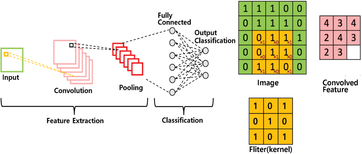
Figure 1: An example of convolutional neural network (CNN) classification structure
A convolution operation is performed by a series of multiplications of weight parameters and input data, followed by accumulating the multiplication results. Fig. 1 shows a convolutional kernel of size 3 × 3 that scans through the image of size 5 × 5 from the top left corner to the right direction and then downwards. First, the convolutional kernel multiplies each pixel within the yellow window by the corresponding weight parameter of the kernel. Then, it accumulates partial products to produce the convolution results as output feature data [4]. The conventional hardware accelerators for the convolution layer often employ an array of parallel multiply-and-accumulate (MAC) operators, which is attributed to the majority of power consumption of the overall CNN accelerator. In an attempt to reduce the power and area of the CNN accelerators, many researchers are adopting mixed-signal approaches [5,6]. To reduce the power consumption and size, this paper introduces an analog convolutional neural network (ACNN) comprising an analog convolutional kernel, an analog max pooling circuit, and a low-power SAR ADC.
An analog convolutional neural network has been introduced in [7]. Fig. 2 illustrates a block diagram of an analog convolutional layer, consisting of 3 analog convolutional kernels, an analog max pooling circuit, and an ADC. In the example of Fig. 2, the three kernels can process three channels for the Red, Green, and Blue colors of the input image. Each of the three convolutional kernels takes nine pixels and nine weight parameters and computes nine multiplications in the current mode. A total of 27 nine multiplications are simultaneously calculated by the three kernels, whose results are accumulated into a capacitor CACC. Once the accumulation is done, the kernel window slides over the image by 1 pixel to the right, downwards, and right. The above operation is repeated by sliding the kernel window to four neighboring pixels. Each of the kernel results is accumulated in the four capacitors respectively. Once the accumulation results of the four kernels are obtained, the analog max-pooling circuit takes the voltage of the four capacitors and selects the highest voltage from the four. Then, the ADC converts the highest voltage from max-pooling into a digital value.
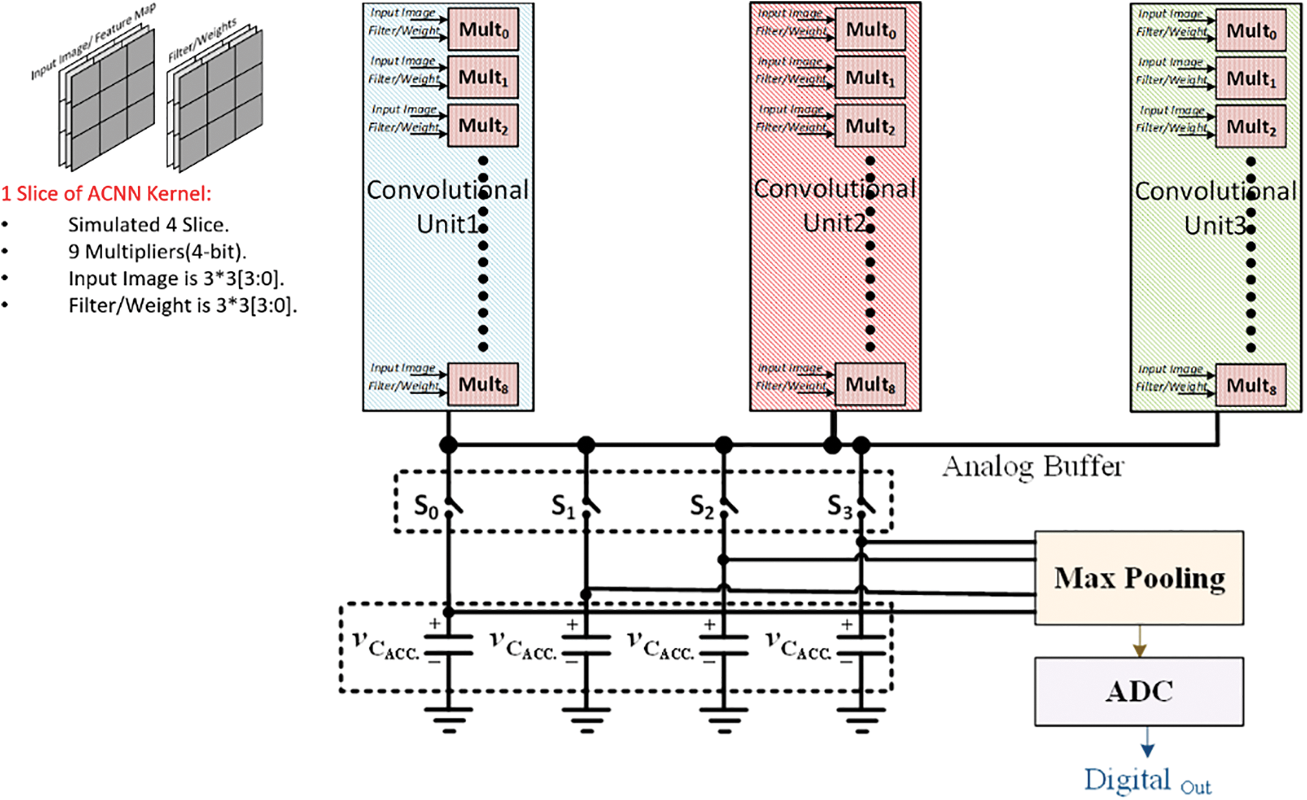
Figure 2: Analog CNN kernel structure including Max pooling
3 Architecture of Proposed 12-Bit SAR ADC
This paper is focused on the ADC specially designed for the analog convolutional kernel. This paper proposes the architecture of SAR ADC with a relatively simple structure and high area and energy efficiency among various ADC types. Capacitor array DAC (CDAC), one of the critical components of the conventional SAR ADC, is composed of Metal-Insulator-Metal Capacitor (MIM Cap). As the resolution increases, the size of the required capacitors increases rapidly, and power consumption increases excessively. Many studies have been conducted to reduce the size and power consumption of these CDACs. Some examples include a method of using a split capacitor array [8], a method of adjusting the magnitude of the supplied reference voltage [9], a method of reducing unnecessary switching in the DAC [10], and a charge recycling method [11]. This paper uses a capacitor array DAC employing split capacitors to reduce CDAC size and power consumption.
SAR ADC requires a sample and hold circuit to stabilize its input voltage. However, the proposed SAR ADC for the ACNN kernel does not require a separate sample and hold circuit because it utilizes the max-pooling circuit as its sample and hold circuit. The 12-bit SAR ADC receives the output voltage of max-pooling as an input and converts the analog value into a digital value by a series of bit decisions through a total of 12 comparisons in the comparator.
Fig. 3 shows the proposed SAR ADC block diagram. The proposed SAR ADC consists of a comparator, SAR logic control, and capacitor array digital-to-analog converter (CDAC). In order to convert the input voltage Vin, the SAR controller successively configures the bit switches of CDAC for a series of 12 cycles and produces the output voltage of CDAC closely matching the max pooling voltage. Eq. (1) models the output voltage Vout of CDAC configured by the SAR controller. It configures the Capacitor ratio of the CDAC to produce Vout that is expressed by Eq. (1). Since the ADC input Vin is the output of MAX Pooling, it is compared with the CDAC output Vout, which starts from the initial voltage of 1/2 Vref and gradually approaching the Vin (voltage value of max pooling output).
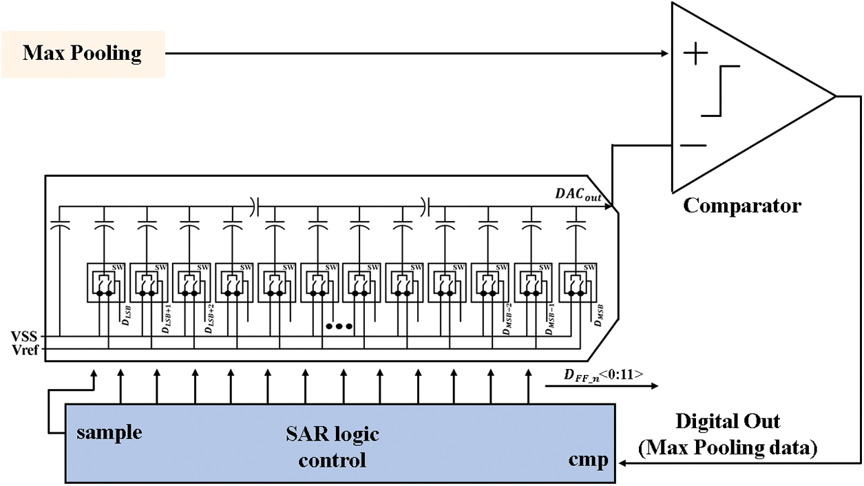
Figure 3: Proposed 12-bit SAR ADC architecture
In Eq. (1), m represents the number of bits of the ADC, while Di represents the i-th bit of the ADC’s digital output. As a result of the comparator, if the Vin value is greater than the CDAC output value, the SAR controller maintains the current digital bit Di as ‘1’. If Vin is smaller, the controller flips Di to ‘0’ and stores it in the output register. The digital conversion is finished upon completing this comparison process for all bits and the digital register provides the final digital value.
3.1 Low-Power Capacitor DAC Design
Fig. 4 shows a basic conventional architecture of 12-bit CDAC. Suppose that the capacitor size for the LSB bit (b = 0) is set to C. Then the size of the capacitors corresponding to the remaining bits b is determined to be
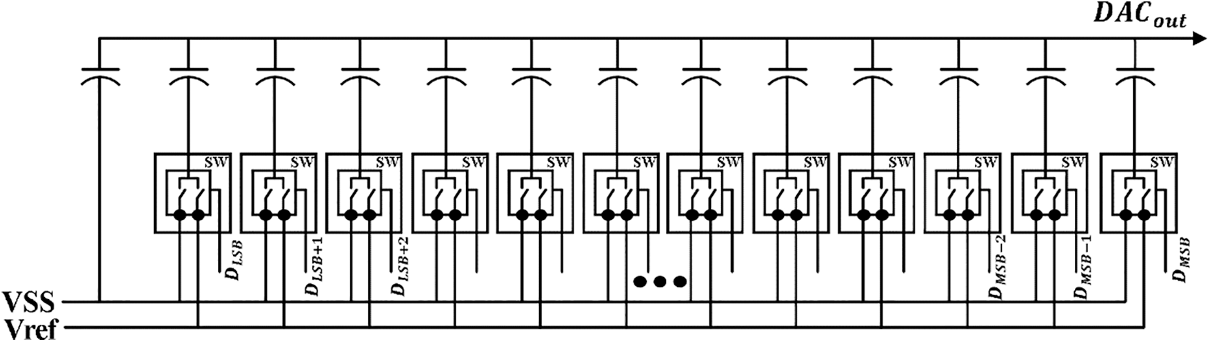
Figure 4: Capacitor array within a standard binary weighted 12-bit CDAC
Fig. 5 shows a compact architecture using a split array structure which inserts a series capacitor called an attenuation capacitor [12]. The attenuation capacitor of size (64/63) C is inserted in a series configuration to split the array into two sub-arrays. The magnitude of the total capacitance of the split array is reduced to (127 + 64/63) C. The value of the attenuation capacitor is determined by Eq. (2).
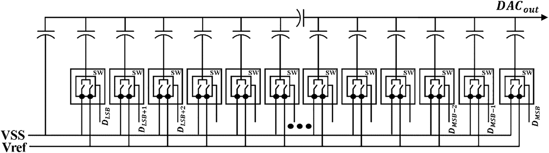
Figure 5: Capacitor array of a 12-bit CDAC with one split capacitor
We can drastically reduce the total capacitor size by inserting more attenuation capacitors into the array. However, as the number of attenuation capacitors increases, the performance of CDAC deteriorates due to the influence of the increasing parasitic capacitance introduced by attenuation capacitors.
Fig. 6 shows the 12-bit CDAC consisting of 3 sub-arrays split up by two attenuation capacitors. The two attenuation capacitors have a size of (16/15) C. The total capacitance of this CDAC array is now reduced to (46 + 32/15) C. The significant decrease in total capacitance offers substantially lower power consumption and faster settling time. However, parasitic capacitance increased in the split capacitor array can deteriorate linearity and the SNDR performance of ADCs.
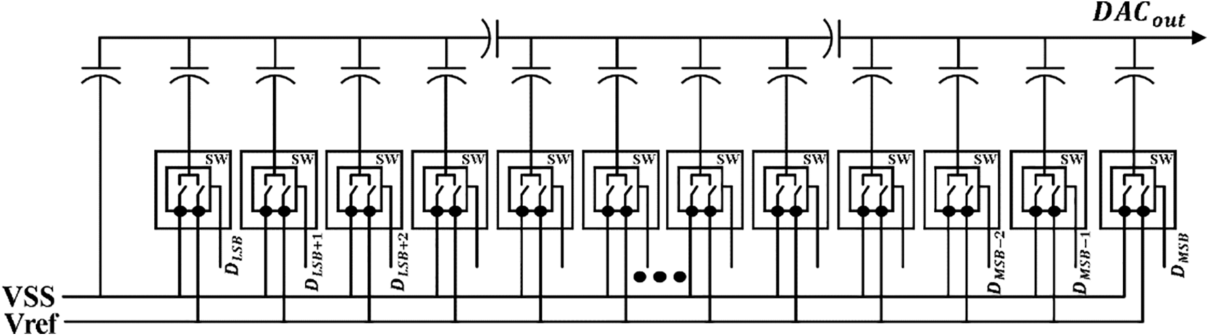
Figure 6: Capacitor array of a 12-bit CDAC with two split capacitors
To optimize linearity, size, and power consumption, we compare capacitors used in CDACs to select capacitors best suited to our target SAR ADC, especially for analog CNN kernel.
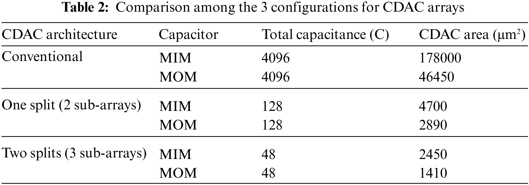
Fig. 7 shows (a) the layout of the metal-oxide-semiconductor (MOS) capacitor, (b) the layout of the metal-oxide-metal (MOM) capacitor, and finally, (c) the layout of the metal-insulator-metal (MIM) capacitor. Table 1 shows the pros and cons, capacitance, and size of each three capacitor types. The MOS capacitors have the highest capacitance density and the smallest size, but their current-voltage (CV) curves show poor linearity. Therefore, they are not suitable for ADCs of high accuracy, where capacitors must maintain constant capacitance over a wide range of voltage changes. On the other hand, MIM capacitors exhibits nearly constant capacitance values regardless of the voltage applied to both ends of the capacitor. However, they suffer from the problem of enormous size. In contrast, MOM capacitors offer relatively high capacitance density with high enough linearity in the CV curve [13]. In this work, therefore, we chose the MOM capacitor type for the 12-bit SAR ADC because we need to minimize its size using multiple split sub-arrays for minimal power consumption and still ensure high enough linearity for high-resolution conversion.
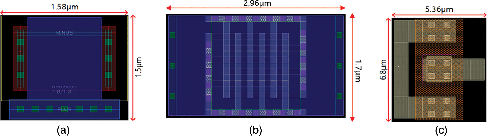
Figure 7: Capacitor layout of (a) MOS capacitor, (b) MOM capacitor and (c) MIM capacitor
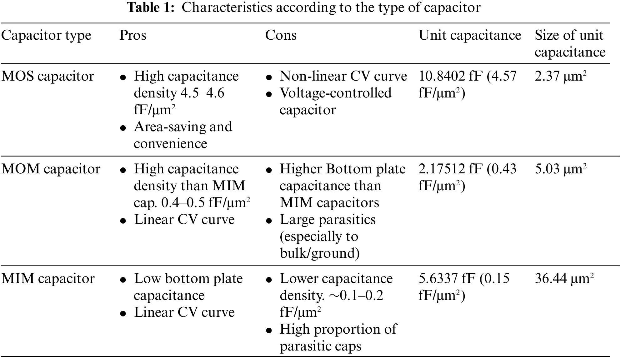
Fig. 8 shows the layout of CDAC of the proposed architecture based on split-array using MOM Capacitors. The total area of this CDAC is 1410 μm2. Table 2 compares three architectures of CDACs: conventional CDAC array, one-spit array, and two-split array. Among the three CDAC architectures, the two-split array is the smallest size. Table 2 compares CDAC designs using MIM and MOM capacitors for each architecture. The CDAC using MOM capacitors is about two times smaller than the CDAC using MIM capacitors. Since the area of CDAC is vital for the whole area of a SAR ADC, we chose the MOM capacitor for CDAC design to reduce both the size and power consumption of the entire target SAR ADC.
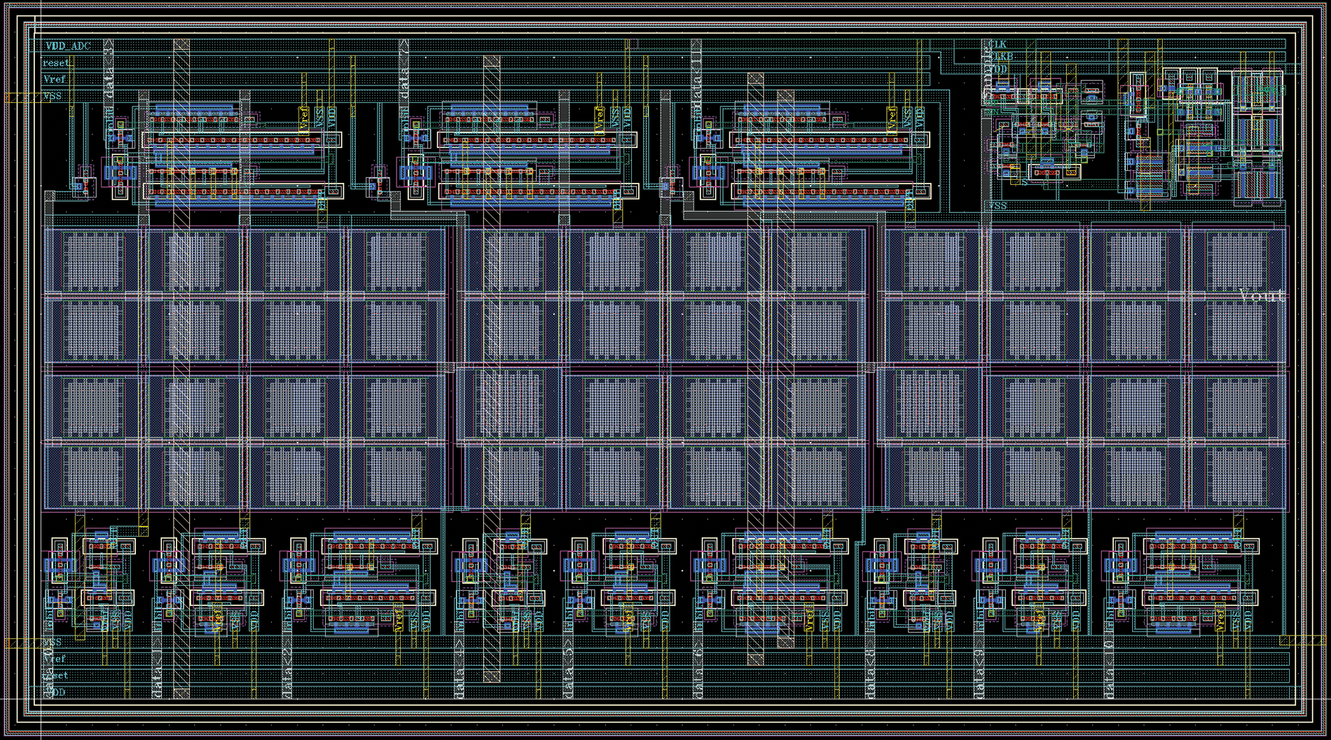
Figure 8: Layout of two split capacitor-array DAC using MOM capacitors
3.2 High Accuracy Low-Power Comparator Design
Conventional latch-based comparators produce a digital output using a latch’s cross-coupled structure with positive feedback. Unfortunately, such comparators suffer from two inherent draws that hinder their performance. First, kick-back noise occurs when a significant voltage variation of the internal node interferes with the input voltage to degrade the performance [14]. Second, the dynamic voltage range of simple latched-based comparators is insufficient due to the limited operating range of transistors in each stage of the comparator, which leads to a loss of signal-to-noise ratio (SNR) [15]. To overcome these drawbacks, this work proposes a comparator that improves SNR by introducing a notion of a complementary dual input stage which significantly increases the dynamic input range without incurring extra power consumption. In addition, the proposed comparator employs a kick-back noise cancellation circuit, further improving SNR.
Fig. 9 shows a circuit of a conventional latch-based comparator with a pre-amplifier. Here, a clock signal (CLK) controls the transistors M4, M5, and M1 in the pre-amplifier stage. This comparator operates in two modes: 1) In the pre-charging step, the output node Out+ and Out− are charged with VDD; 2) In the evaluation step, (a) if Vin+ is higher than Vin−, then the load capacitor at M3 discharges faster than that at M2 until it reaches the threshold voltage of M11 causing it to turn off. Therefore, the output node Out− is ‘0’ and the output node Out+ is ‘1’. (b) If Vin− is higher than Vin+, then the load capacitor at M2 discharges faster than that at M3 until it reaches the threshold voltage of M10 causing it to turn off. Therefore, the output node Out+ is ‘0’ and the output node Out− is still ‘1’ [16]. However, as the input values of Vin+ and Vin− approach VDD, the discharge rate of the two load capacitors becomes virtually the same. Eventually the voltages of node A and node B become the same. Therefore, if a PMOS-based latch-type comparator is used, the input range of the comparator is limited to VDD-|VTHP| in VSS.
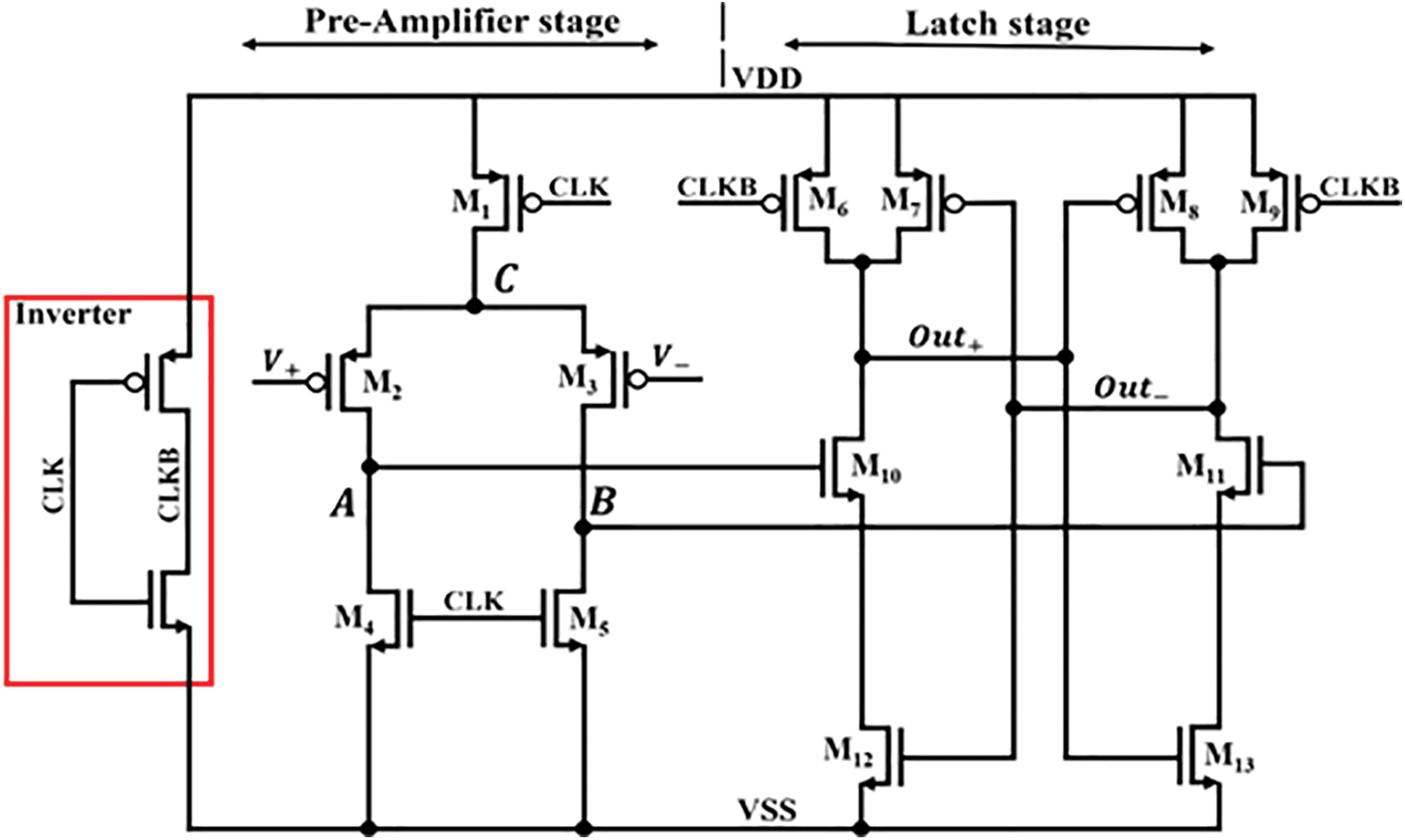
Figure 9: Conventional latch-based comparator with pre-amplifier
Fig. 10 shows the simulation result for Node A and Node B when 1 and 1.1 V are given as inputs. It discloses the problem that the discharge speed of the two load capacitors at nodes A and B is nearly the same as the two inputs approach the maximum voltage of 1.2 V (VDD). Thus, the comparator cannot tell the difference between the input voltages. Therefore, although the conventional latch-based comparator of Fig. 9 has the advantage of low power, its simplistic differential input pair incurs severe limitations in that it cannot distinguish the two inputs when the inputs approach the maximum voltage (VDD).
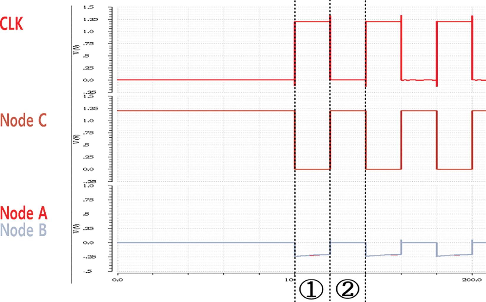
Figure 10: Simulation result of the dynamic comparator with pre-amplifier
Fig. 11 shows the circuitry of the rail-to-rail latch-based comparator with a pre-amplifier [17]. This comparator has a wide input range because it receives input through two differential pairs of PMOS and NMOS types, but it suffers from high power consumption due to more current paths.
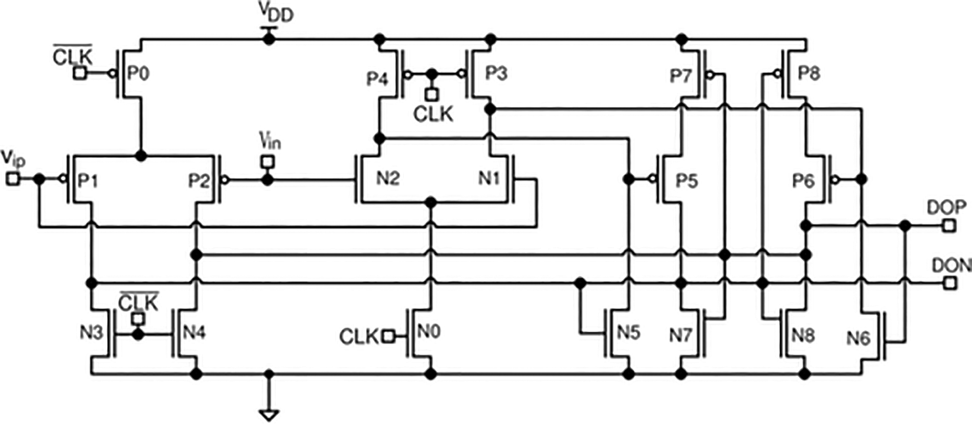
Figure 11: Rail-to-rail latch-based comparator
To overcome the drawbacks of the exiting comparators, this work proposes a new comparator which introduces a complementary structure of dual input transistors in the pre-amplifier stage and is shown in Fig. 12. In order to ensure that the two input paths have different discharge rates even when the two inputs are close to the maximum voltage, complementary transistors M2a and M3a are added. These transistors receive inputs opposite to the existing two inputs. The proposed comparator offers the advantages of low power and compact size since it uses only a single differential pair in the pre-amplifier stage, along with the rail-to-rail input range.
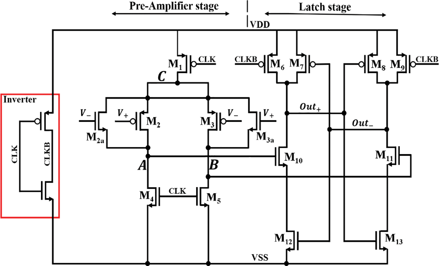
Figure 12: Proposed complementary dual input rail-to-rail Comparator
Fig. 13 shows the simulation results for Node A and Node B when the two inputs are very close to VDD, for example, 1 and 1.1 V, respectively. It can be observed that the discharge speeds of the load capacitors at nodes A and B are different. Therefore, the voltage at Node A is higher than Node B, so output Out+ becomes ‘0’ while output Out− is ‘1’.
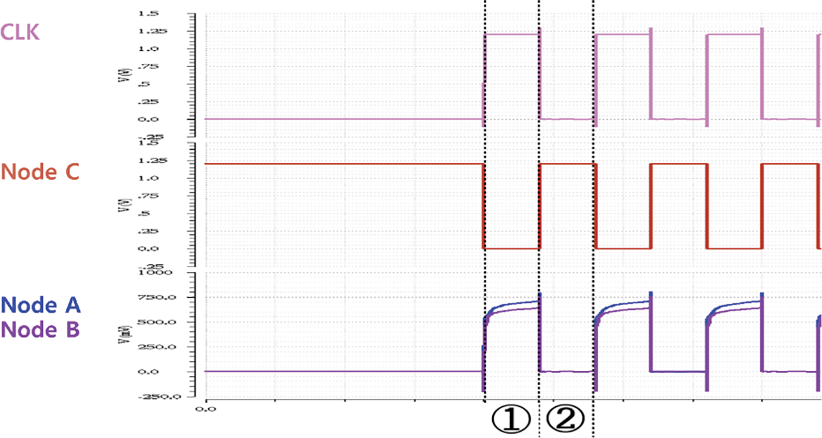
Figure 13: Simulation results of the proposed complementary dual input rail-to-rail dynamic comparator with pre-amplifier
Fig. 14 shows the simulation results of converting the digital output value from SAR ADC for ramp input (Vin) into analog value (Ideal_DAC_out) using an ideal DAC. The input range is from VSS to 1.0 V, over which the output of the ideal DAC is compared against ramp input. Fig. 14a shows the result of the conventional comparator of Fig. 9, while Fig. 14b show the result of the proposed comparator of Fig. 12. Due to its simplistic PMOS differential pair, the conventional comparator of Fig. 14a stops correct operation and saturates at a voltage of 915 mV and above. In contrast, Fig. 14b shows that the proposed comparator correctly operates from VSS to 1.0 V, extending the operational range significantly by 9.2% compared to the conventional comparator.
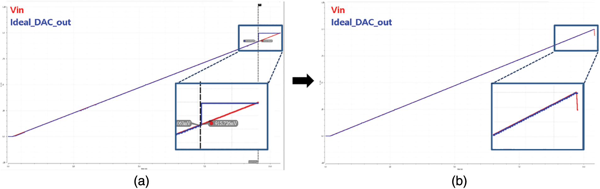
Figure 14: Simulation results of the ADC followed by an ideal DAC for the ramp function (a) using a conventional comparator, and (b) using the proposed the comparator
3.3 Reducing Kick-Back Noise of Comparator
Kick-back noise is one of the causes that degrade the accuracy of the SAR ADC [18]. When a significant voltage variation, like a clock signal, is applied to an internal node that carries the input signal, the kick-back noise occurs and deteriorates the input voltage. Fig. 15 shows the output voltage of the CDAC that is provided to the comparator as input. In Fig. 15 at (c), if the voltage at the internal node fails to return to its original voltage until the next clock, it is not easy to compare the exact values in the comparator. In this work, to reduce this problem, we introduce a method that cancels the kick-back noise by generating kick-back noise of opposite phases through a dummy input circuit [19].
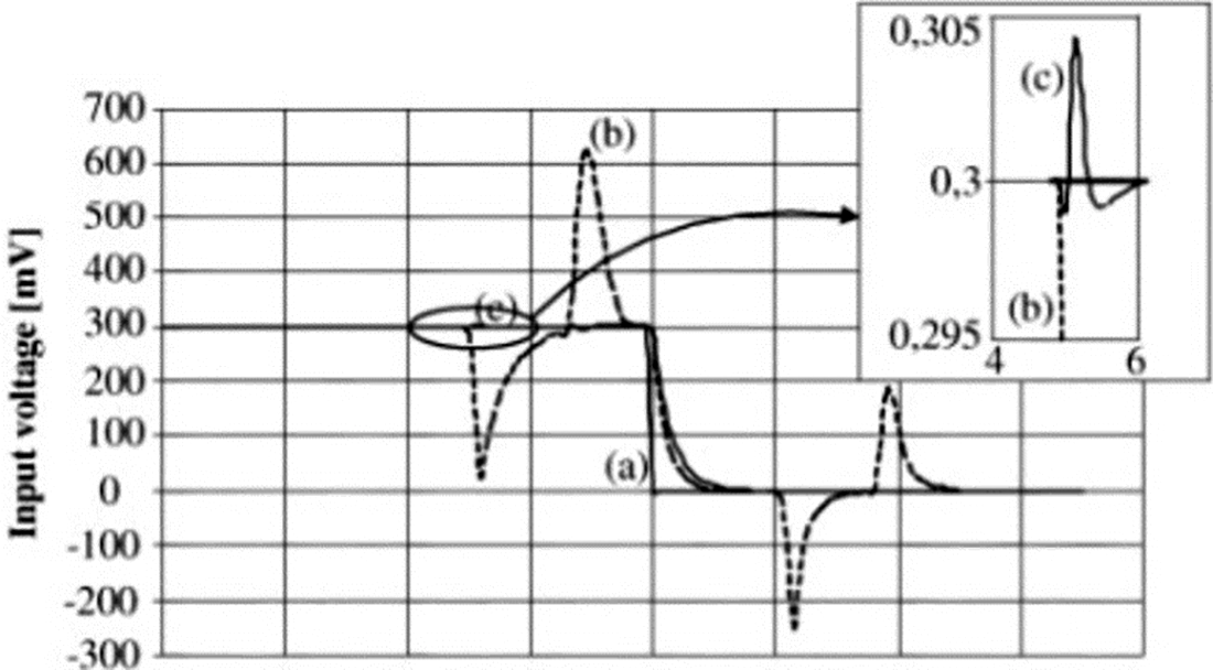
Figure 15: The output results of CDAC
Fig. 16 illustrates the kick-back noise reduction circuit, which adds a dummy capacitor each at the two inputs of the pre-amplifier stage of the comparator input terminals. The dummy capacitors are formed by transistors M1d and M2d. First, using transmission gates triggered by CLK and CLKB, signals of the opposite phase to kick-back noise are applied to pre-charge the dummy capacitors. Next, these oppositely phased signals are added into the two complementary input voltages, V+ and V−. This addition of noise at the input terminals will cancel out the internal node’s voltage variations. Hence the input voltage will not deteriorate, and the Kick-back noise effect will be minimized.
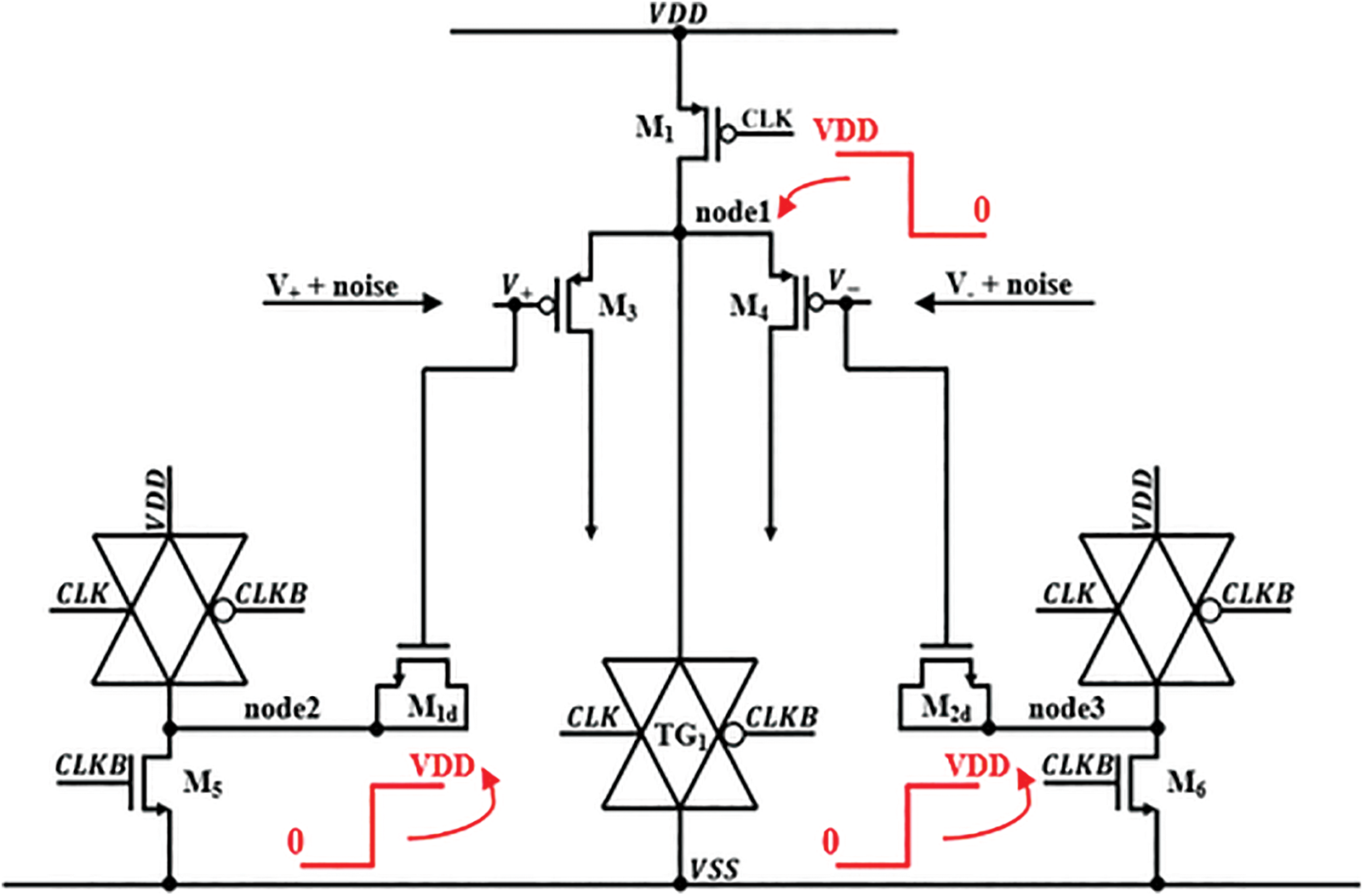
Figure 16: Kick-back noise reduction circuit
Fig. 17 shows the output of the CDAC, which becomes the input of the comparator. Fig. 17a shows the simulation results of the comparator without the cancellation circuit where CDAC_out is deteriorated by kick-back noise for about 2.08 mV. Fig. 17b shows the simulation results of the comparator with the proposed cancellation circuit, where kick-back noise is reduced by about 40% to about 1.27 mV. Due to the decrease in kick-back noise, the ENOB of the proposed 12-bit SAR ADC increases by more than 10% from 10.2 to 11.07 bits.
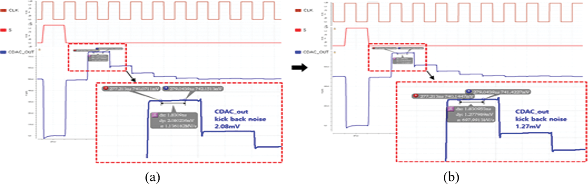
Figure 17: Simulation of the CDAC output (a) before removing the noise (b) after removing the noise
3.4 Analog Convolution Neural Network Kernel Using ADC
Fig. 18 shows the simulation results of an analog convolutional neural network (ACNN) where the proposed ADC is applied. It consists of a total of three units of analog convolutional kernel units (ACUs), each comprising nine analog multipliers. Each analog multiplier takes input image pixel data A [0:3] and filters weights B [0:3]. The three ACUs produce the sum of the multiplications in the form of current. The total current amount from the three ACUs is accumulated in one of the four capacitors CACC to produce output in the form of voltage VCACC, as illustrated in Fig. 18. The above convolutional computation is repeated for 4 four stride movements (stride by one pixel) of filter data over input image data sequentially, starting from upper left corner then moving right, downwards and left. Multiplication results from three ACUs in the form of current are accumulated over each capacitor corresponding to the respective stride movement. Once the four capacitors are charged with four voltages VCACC through the four repeated convolution computations, the analog max-pooling circuit selects the highest voltage among the four. For the example of Fig. 18, the voltage values produced by the four accumulation capacitors are 423, 554, 438, and 356 mV, respectively. The highest voltage, 555 mV, becomes the output value of the max-pooling circuit. This highest voltage value is then converted to a digital value of 100011100111 by the proposed ADC. For verification, this digital value is converted back to an analog voltage by an ideal DAC. The analog voltage value is 556 mV showing an error of only 1 mV, thus verifying the high accuracy of the proposed ADC.
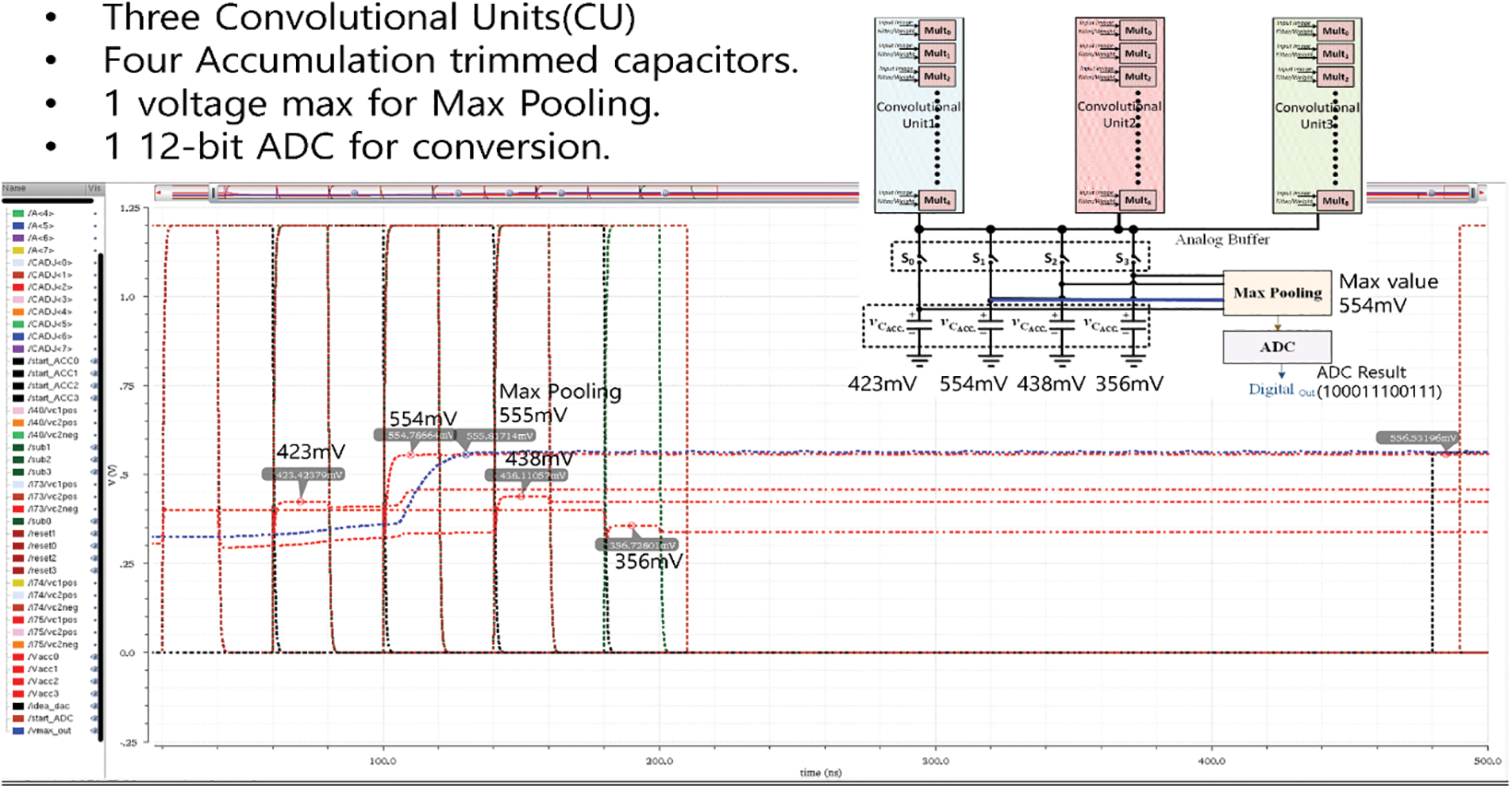
Figure 18: Simulation of analog multiply-and-accumulate for CNN kernel
4.1 Implementation of the Proposed 12-Bit SAR ADC
The proposed 12-bit SAR ADC was designed using a 55 nm CMOS process. Fig. 19 shows the pre-layout simulation results of the SAR ADC. The simulation environment in which performance analysis was performed is as follows. The unit capacitance C of the capacitor array was chosen to be 5.56 fF, which leads to the compact size of 268 fF for capacitor array DAC. For both analog and digital circuits, the supply voltage was 1.2 V. The input range of the ramp function was set to 0 to 1 V, the reference voltage Vref to 1 V, and the sampling rates to 17.857 MHz. In Fig. 19, data_<0> to data_<11> indicates the digital output values of the SAR ADC. As a result of analyzing the performance of ADC after converting these digital output values to analog voltage using ideal DAC, the observed Differential Non-Linearity (DNL) was −0.48/+0.50 LSBs, and the Integral Non-Linearity (INL) was −0.49/+0.58 LSBs.
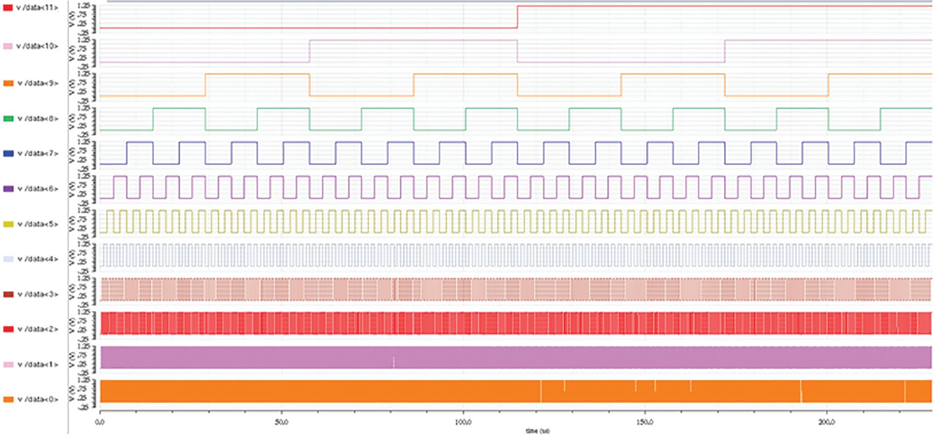
Figure 19: Simulation of 12-bit SAR ADC
Fig. 20 shows the output spectrum with a coherent frequency input
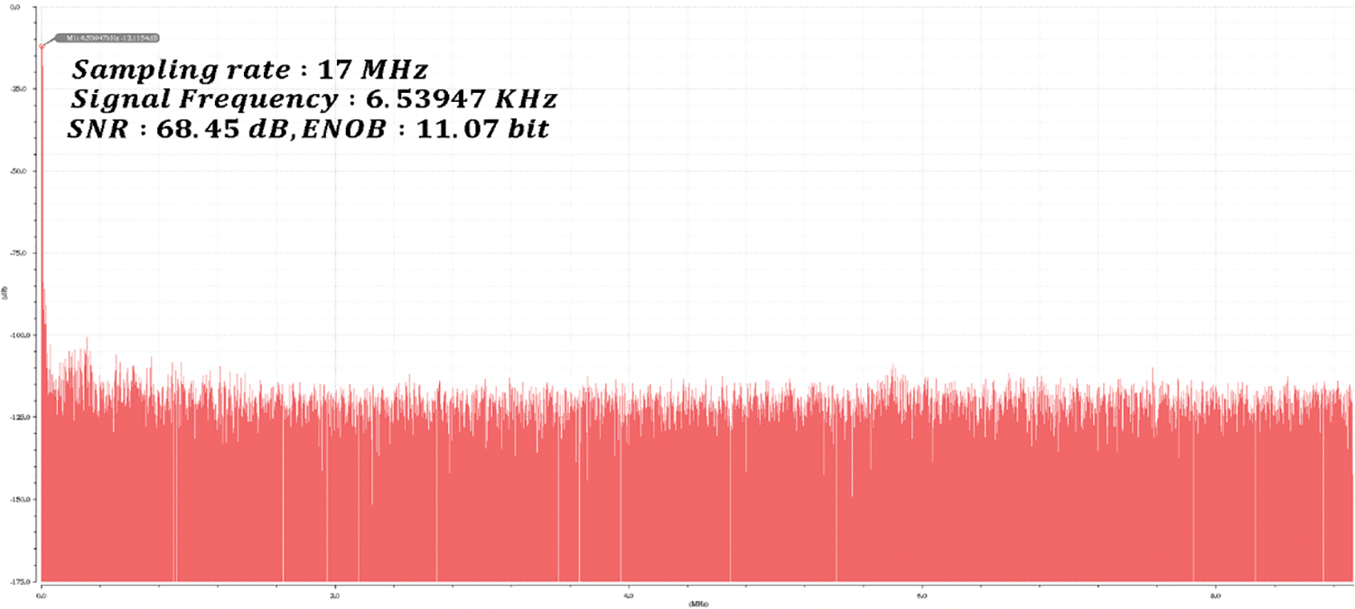
Figure 20: Output spectrum result of proposed 12-bit SAR ADC
Here,
4.2 Implementation of Analog CNN Test Chip
A test chip was implemented to analyze the performance of the SAR ADC and verify the overall behavior of the mixed-signal convolutional neural network accelerator. The test chip was a mixed-signal convolution neural network accelerator chip supporting a convolution filter with three concurrent channels of 3 × 3 kernels It was fabricated using a TSMC CMOS 55 nm process. The test chip was implemented by integrating the proposed SAR ADC with an analog convolutional kernel and a max pooling circuit described in Figs. 2 and 18. The analog convolution kernel consists of 3 analog convolution kernels to realize the convolution layer of the CNN. Each analog kernel comprises nine multiply-and-accumulate (MAC) units which multiply 3 × 3 input image pixels with 3 × 3 weights elementwise and produces the resulting current as the multiplication outputs. Therefore, the total number of analog multiply units is 27, whose outputs are summed by the accumulator circuit and stored in each capacitor. The max pooling circuit selects the highest value among the four capacitor voltage values, while the ADC converts it to a digital value to store in memory.
Fig. 21 shows the entire chip layout of the two sub-test chips: the first sub-test chip of the proposed SAR ADC and the second sub-test chip of the analog CNN accelerator, including the proposed SAR ADC. The first sub-test chip for SAR ADC consists of a CDAC array with split sub-arrays, SAR control logic, and a sample-and-hold circuit. The second sub-test chip integrates analog convolutional kernels, accumulation capacitors, a max-pooling circuit, a 12-bit SAR ADC and a digital controller.
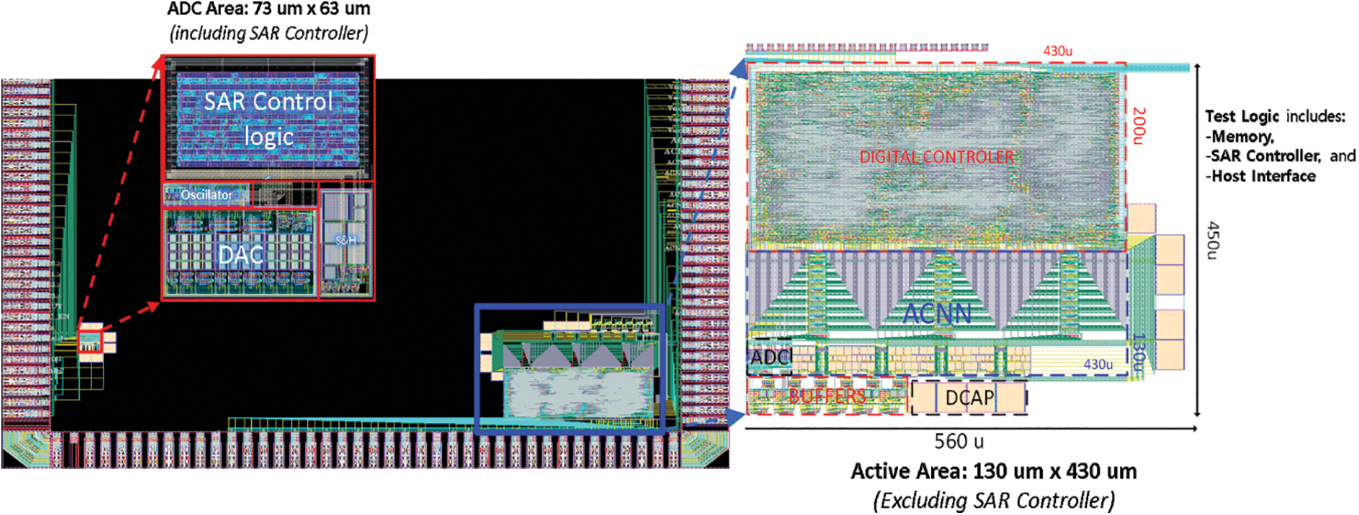
Figure 21: Layout implemented for ACNN and SAR ADC
Table 4 shows the chip area and power consumption of the mixed-signal analog convolution kernel design consisting of a 3 × 3 analog convolution kernel, a max pooling, and the proposed 12-bit SAR ADC in comparison with the full-digital convolution kernel design. It can be observed that the mixed-signal convolution kernel reduces the chip area by 85% and power consumption by 79% compared to the digital convolution kernel.
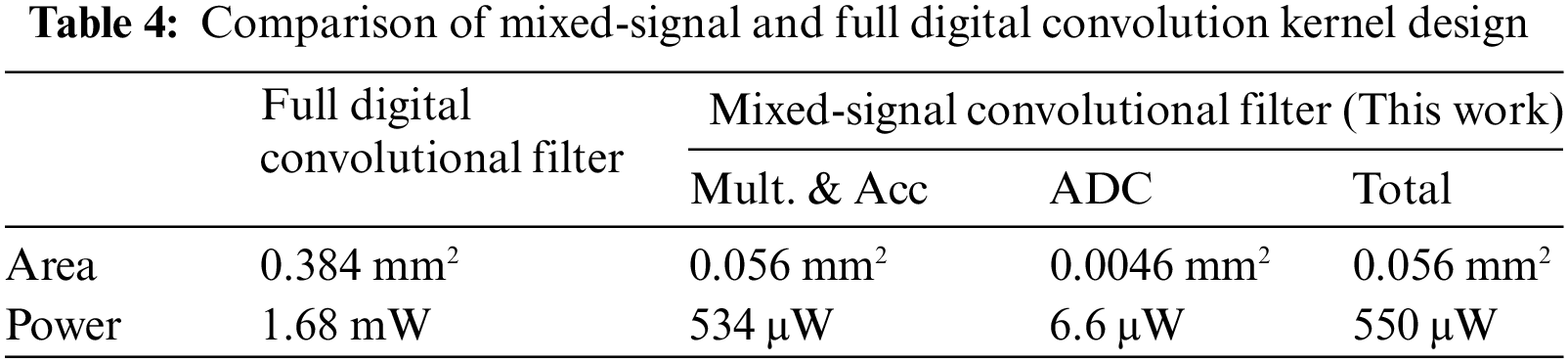
Fig. 22 compares the growth trend in the area and power consumption of the analog convolution kernel and the digital convolution kernel when the size of the convolution filter gradually increases from 3 × 3 to 15 × 15. In the case of digital convolution, when a filter more than 3 × 3 is used, the area and power increase quadratically due to the 2D array structure of the digital multipliers, while in the case of analog convolution filter, the area increases very smoothly.
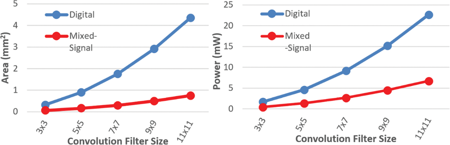
Figure 22: Mixed-signal and digital design comparison for area and power consumption
Since most existing convolutional neural network accelerator chips were designed using digital convolution filters, they need more power consumption and chip size. Until now, analog approaches to convolution kernel circuits have received limited attention due to the overhead of large ADCs or the lack of techniques for improving their accuracy. This paper, in contrast, presented a minimal but highly accurate SAR-ADC design enlightening the alternative roadmap to mixed-signal designs for CNN accelerators.
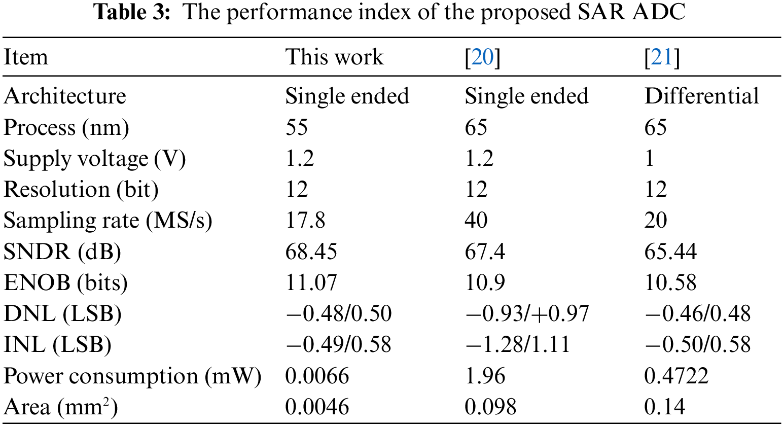
This paper proposes a SAR ADC design optimized for size, power and accuracy targeting for Analog convolutional neural network chips. A low-power 12-bit SAR ADC is proposed using a split capacitor array with three sub-arrays. We also analyzed various capacitor types and selected the MOM capacitor, which offers relatively high capacitance density at the sacrifice of linearity to trade-off between power and accuracy. Design techniques for maximizing the dynamic input range and minimizing the kick-back noise in the comparator of the ADC were presented, which helped to overcome the accuracy loss of the split capacitor array and offered higher SNDR and ENOB. The proposed SAR ADC occupied 4.6 um2 and consumed 6.6 uW power.
To further demonstrate the effectiveness of the proposed ADC, we integrated the ADC into the entire test chip with an analog CNN chip. The analysis of the test chip unveiled that the chip area and power consumption were significantly reduced compared to a conventional CNN accelerator chip designed only for the digital circuit: the chip area was reduced by 85%, and power consumption was reduced by 79%. Therefore, the findings in this study on an optimal design of SAR ADC and its application to the mixed-signal neural network accelerator chip are encouraging and illuminating pioneering paths to ultra-low power CNN accelerator realizations for future mobile AI applications.
Funding Statement: This work was supported by the National Research Foundation of Korea (NRF) grant funded by the Korea government (MSIT) (No. 2022R1A5A8026986), and supported by Institute of Information & communications Technology Planning & Evaluation (IITP) grant funded by the Korea government (MSIT) (No.2020-0-01304, Development of Self-learnable Mobile Recursive Neural Network Processor Technology). It was also supported by the MSIT (Ministry of Science and ICT), Korea, under the Grand Information Technology Research Center support program (IITP-2022-2020-0-01462) supervised by the “IITP (Institute for Information & communications Technology Planning & Evaluation)” and supported by the National Research Foundation of Korea (NRF) grant funded by the Korea government (MSIT) (No. 2021R1F1A1061314). In addition, this work was conducted during the research year of Chungbuk National University in 2020.
Conflicts of Interest: The authors declare that they have no conflicts of interest to report regarding the present study.
References
1. J. Y. Lee, M. S. Asghar, S. Arslan and H. Kim, “Low power ADC design for mixed signal convolutional neural network accelerator,” Journal of the Korea Institute of Information and Communication Engineering, vol. 25, no. 11, pp. 1627–1634, 2021. [Google Scholar]
2. T. Homma, L. E. Atlas and R. J. Marks, “An artificial neural network for spatiotemporal: Application to phoneme classification,” in Proc. Int. Conf. on NIPS, Cambridge, MA, USA, pp. 31–40, 1987. [Google Scholar]
3. M. S. Asghar, S. Arslan and H. Kim, “A low-power spiking neural network chip based on a compact LIF neuron and binary exponential charge injector synapse circuits,” Sensors, vol. 21, no. 13, pp. 4462, 2021. [Google Scholar] [PubMed]
4. Machine-Geon, Convolution neural network (CNN), 2019. [Online]. Available: https://machine-geon.tistory.com/46 [Google Scholar]
5. J. Choi, S. Lee, Y. Son and S. Y. Kim, “Design of an always-on image sensor using an analog lightweight convolutional neural network,” Sensors, vol. 20, no. 11, pp. 3101, 2020. [Google Scholar] [PubMed]
6. M. Z. Wong, B. Guillard, R. Murai, S. Saeedi and P. H. J. Kelly, “AnalogNet: Convolutional neural network inference on analog focal plane sensor processors,” arXiv:2006.01765 [cs, eess], Jun. 2020, Accessed: Nov. 08, 2020. [Online]. Available: http://arxiv.org/abs/2006.01765 [Google Scholar]
7. M. S. Asghar, M. Junaid, H. W. Kim, S. Arslan and S. A. Ali Shah, “A digitally controlled analog kernel for convolutional neural networks,” in Proc. ISOCC, Jeju Island, Republic of Korea, pp. 242–243, 2021. [Google Scholar]
8. H. Kang, S. Asmat Ali Shah and H. Kim, “An energy-efficient 12b 2.56 ms/s sar adc using successive scaling of reference voltages,” Computers, Materials & Continua, vol. 72, no. 1, pp. 2127–2139, 2022. [Google Scholar]
9. V. Hariprasath, J. Guerber, S. H. Lee and U. K. Moon, “Merged capacitor switching based SAR ADC with highest switching energy-efficiency,” Electronics Letters, vol. 46, no. 9, pp. 620–621, 2010. [Google Scholar]
10. B. P. Ginsburg and A. P. Chandrakasan, “An energyefficient charge recycling approach for a SAR converter with capacitive DAC,” 2005 IEEE International Symposium on Circuits and Systems, vol. 1, pp. 184–187, 2005. [Google Scholar]
11. L. Sun, B. Li, A. K. Y. Wong, W. T. Ng and K. P. Pun, “A charge recycling SAR ADC with a LSB-down switching scheme,” IEEE Transactions on Circuits and Systems I: Regular Papers, vol. 62, no. 2, pp. 356–365, 2015. [Google Scholar]
12. A. Ahuja, K. Badami, C. Barbelenet and S. Emery, “Comparison of capacitive DAC architectures for power and area efficient SAR ADC designs,” in Proc. ISCAS, Daegu, Korea, pp. 1–5, 2021. [Google Scholar]
13. Utmel Electronics, What is the difference between MOM, MIM and MOS capacitors, 2021. [Online]. Available: https://www.utmel.com/blog/categories/capacitors/what-is-the-difference-between-mom-mim-and-mos-capacitors [Google Scholar]
14. Y. Huang, H. Schleifer and D. Killat, “Design and analysis of novel dynamic latched comparator with reduced kickback noise for high-speed ADCs,” in Proc. ECCTD, Dresden, Germany, pp. 1–4, 2013. [Google Scholar]
15. S. Lan, C. Yuan, Y. Y. H. Lam and L. Siek, “An ultra-low-power rail-to-rail comparator for ADC designs,” in Proc. MWSCAS, Seoul, Korea, pp. 1–4, 2011. [Google Scholar]
16. D. Yasser, M. A. ElGamal, M. Atef, O. Hamada, A. H. Hassan et al., “A comparative analysis of optimized low-power comparators for biomedical-ADCs,” in Proc. ICM, Beirut, Lebanon, pp. 1–4, 2017. [Google Scholar]
17. S. B. Kobenge and H. Yang, “A 250KS/s, 0.8V ultra low power successive approximation register ADC using a dynamic rail-to-rail comparator,” IEICE Electronics Express, vol. 7, no. 4, pp. 261–267, 2010. [Google Scholar]
18. P. M. Figueiredo and J. C. Vital, “Kickback noise reduction techniques for CMOS latched comparators,” IEEE Transactions on Circuits and Systems II: Express Briefs, vol. 53, no. 7, pp. 541–545, 2006. [Google Scholar]
19. A. Varzaghani, A. Kasapi, D. N. Loizos, S. -H. Paik, S. Verma et al., “A 10.3-GS/s, 6-bit flash ADC for 10G ethernet applications,” IEEE Journal of Solid-State Circuits, vol. 48, no. 12, pp. 3038–3048, 2013. [Google Scholar]
20. I. Yeo and B. G. Lee, “A 12-bit 40 MS/s SAR ADC with digital foreground self-calibration for capacitor mismatches,” Journal of Semiconductor Technology and Science, vol. 20, no. 1, pp. 105–118, 2020. [Google Scholar]
21. K. Shehzad, D. Verma, D. Khan, Q. U. Ain, M. Basim et al., “A low-power 12-bit 20 MS/s asynchronously controlled SAR ADC for WAVE ITS sensor based applications,” Sensors, vol. 21, no. 7, pp. 2260, 2021. [Google Scholar] [PubMed]
Cite This Article
 Copyright © 2023 The Author(s). Published by Tech Science Press.
This work is licensed under a Creative Commons Attribution 4.0 International License , which permits unrestricted use, distribution, and reproduction in any medium, provided the original work is properly cited.
 Downloads
 Citation Tools