
 Submit a Paper
 Propose a Special lssue
 Open Access
ARTICLE
A Scalable Interconnection Scheme in Many-Core Systems
Computer Systems Engineering, Arab American University, Jenin, 240, Palestine
* Corresponding Author: Allam Abumwais. Email:
Computers, Materials & Continua 2023, 77(1), 615-632. https://doi.org/10.32604/cmc.2023.038810
Received 30 December 2022; Accepted 14 April 2023; Issue published 31 October 2023
 View Full Text
 Download PDF
Abstract
Recent architectures of multi-core systems may have a relatively large number of cores that typically ranges from tens to hundreds; therefore called many-core systems. Such systems require an efficient interconnection network that tries to address two major problems. First, the overhead of power and area cost and its effect on scalability. Second, high access latency is caused by multiple cores’ simultaneous accesses of the same shared module. This paper presents an interconnection scheme called N-conjugate Shuffle Clusters (NCSC) based on multi-core multi-cluster architecture to reduce the overhead of the just mentioned problems. NCSC eliminated the need for router devices and their complexity and hence reduced the power and area costs. It also resigned and distributed the shared caches across the interconnection network to increase the ability for simultaneous access and hence reduce the access latency. For intra-cluster communication, Multi-port Content Addressable Memory (MPCAM) is used. The experimental results using four clusters and four cores each indicated that the average access latency for a write process is 1.14785 ± 0.04532 ns which is nearly equal to the latency of a write operation in MPCAM. Moreover, it was demonstrated that the average read latency within a cluster is 1.26226 ± 0.090591 ns and around 1.92738 ± 0.139588 ns for read access between cores from different clusters.Keywords
In multiprocessor systems and multi-core processors afterward, the processors (the cores) of the system compete for access to the shared resources, mainly the interconnection networks and the shared memory. They compete during the execution of the main program instructions and the execution of the cache coherence protocols instructions. This competition leads to contention, arbitration, bottleneck, and time delay as a result. Due to these problems, a longer execution time of the program is expected. In the previous papers, the authors have presented an organization that rids the system of these problems [1–3].
During the past decade, processor designers started working on expanding the multi-core systems to many-core systems where the latter contains a large number, tens to hundreds, of cores [4–6] and they developed several many-core systems over the last few years [7–9]. Because the Interconnection networks architecture is at the core of such systems, various architectures have been proposed in the literature. Network on Chip (NoC) router-based architecture becomes the optimal solution to overcome the long-standing challenges for traditional bus interconnection networks due to many features such as scalability, effective bandwidth, and others. The NoC that uses routers to provide multiple paths between cores to enhance throughput and scalability has two schemes; buffered and buffer-less NoCs. Recently, most research groups work to improve the performance of these schemes by producing a hybrid NoC which merges between buffered and buffer-less NoC to handle distributed resources in many-core systems, and reduce the contentions, power consumption and so provide high-efficiency NoC [10,11].
All many-core interconnection network that uses router-based NoC pays a heavy penalty in terms of area and power consumption due to the complex router structure. Research revealed that routers’ structure in mesh or tour topology consumes about 28% of the total power and 17% of the total area in the Intel chip [12]. In addition, the structure of routers puts additional latency due to the increase in hardware structures that negatively affect the performance. Hence this reduces the scalability. On the other hand, there is still a bottleneck when more than one core simultaneously accesses the same shared cache module because this increases the access latency and hence degrades the system performance.
Designing an effective network topology that reduces the penalties that may be produced in a large-scale system is the main contribution of this paper. Therefore, the goal of this paper is to present a router-less high-effective interconnection network topology based on a multi-cluster architecture capable of improving performance metrics like scalability, size, bandwidth, complexity, and latency. It addresses the scalability problem caused by router structure and reduces the shared cache access latency.
In this paper, an interconnection scheme called NCSC that connects N multi-core clusters each of which consists of n cores, where (n ≥ N), is presented and authors assume that n = N i.e., N2 cores are included in the proposed system. This design consists of two parts. MPCAM organization for communication cores within the same cluster, and conjugate shuffle interconnection for inter-cluster communication. NCSC eliminates the routers devices from both parts leading to an increase in the system scalability. Also, redesigned shared cache organization and distributed across the interconnection network; to increase the ability for simultaneous access and hence reduce the access latency.
The remaining of this paper is organized as follows: Section 2 briefly lists the literature review for many-core interconnection networks. Section 3 explains the main component of the proposed interconnection networks within a cluster and inter-clusters. Section 4 discusses the implementation of the NCSC in Field Programmable Gate Arrays (FPGA) while Section 5 displays the main parts simulation and demonstrates the latency estimation analysis in different scenarios. Finally, Section 6 draws some conclusions from this study and suggests a future vision.
Because of the router-based NoC problems, researchers start with the strenuous pursuit to reduce the number of routers and then produce a router-less NoC. Awal et al. [13] proposed a combination of 2-D mesh on multilayers NoC. It reduces the number of routers needed in the network based on multilayers chip. This network has several attractive metrics, such as network cost, and constant degree. Compared to other interconnection networks, it has moderate latency, fault-tolerant structure, and link count. Whilst this interconnection network has several attractive metrics, it has a drawback of the difficulty to scale the design because this requires additional chip layers making it not feasible in current technology. Moreover, this architecture does not take into account the connection of the cores to shared memory.
Li et al. [14] proposed Nesting Ring NoC (NRO). This topology consists of a set of clusters each with a fixed size of four cores. NRO achieves attractive features in terms of performance and latency but it has an obvious problem in terms of scalability specifically as the number of cores increases to hundreds or more. This will increase the network diameter causing higher delays and increased traffic along inter-cluster paths. In [15] authors try to address these problems using a large-scale NRO interconnection network that modifies NRO in two ways. First, by introducing new links between cores and clusters to reduce the network diameter. Second, by exploiting the advantages of multilevel chips to combine large cores on each cluster. On the other hand, this work does not discuss the shared memory issue between Intra and inter-clusters.
Udipi et al. [6] designed a new interconnection structure that eliminates the routers between segments. This architecture is based on a shorted bus and a segmented bus. The main idea is to divide the system chip into various segments of cores, with a shorted bus interconnection on each segment. Each sub-segment bus is connected to a central bus that is directly connected to the manager core. A simple control unit, called “Filter”, was implemented on each central bus to allow the data to transmit between segments. This design has a scalability problem because large numbers of cores need large links and complex control units especially to preserve consistency for shared cache memory.
Liu et al. [16] proposed a new architecture called Isolated Multi-Ring (IMR) that tries to connect up to 1024 cores with Multi-Ring topology. In IMR, any two cores can be connected via one or more isolated rings so that each packet can reach the destination directly by the same ring structure. This eliminates the need for complex routers and so improves performance and reduces hardware costs. IMR enhanced the throughput and latency but still has many issues like a large number of rings and a large number of buffers at interfaces.
Alazemi et al. [17] proposed a novel router-less architecture that exploits the bus’s resources perfectly to achieve the shortest path and solve the scalability problem. As the new technologies scale the chips to smaller dimensions, it supports a higher level of metal layers for integration. With this new trend, the increasing number of layers will be exploited in routing metal layers. For example, The Intel Xeon Phi series are designed in 13 metal layers [18]. The simulation results show that this architecture achieves a significant advantage in latency, performance, and power consumption. Whilst this idea is so promising, the specific architecture has several issues and deals with ideal many-core architecture without taking into consideration issues related to shared caches.
The authors in [19,20] proposed a new machine learning based on the deep reinforcement method, to decide on the ideal loop placement for routerless NoCs under different design restrictions. The new approach successfully solves issues with the old design, but it still uses a lot of interconnection loops, which increases power consumption.
The cache coherence protocols cause a larger delay because each core must notify other cores of any changes it makes to a shared variable. The authors in [3] suggested a new coherency approach in the MPCAM that guarantees the cache coherence for all shared variables over multi-core. With this method, there is no longer a need for cache coherence operations, and the delay of accessing the shared cache becomes the same as accessing the core’s private memory.
This literature contributes to the research topic: router-less interconnection network in a many-core architecture. The main goal of this article is to propose an effective interconnection network, which improves many-core performance by exploiting MPCAM shared memory and router-less techniques.
3 The Component of the Proposed Scheme
During the early stages of the proposed NCSC design, the decision was taken that using a router device is not a choice, because it adds burden and complexity to network architecture. NCSC uses N-shuffle stages connected by N crossbar network-based clusters; each consists of N processors. N-shuffle stages have been used before in many interconnection networks [21–23]. This scheme has been modified to an N-conjugate shuffle to meet the design needs of multi-cluster connection, where the conjugate core (manager core) in each cluster is responsible for inter-cluster communication. Combining N-conjugate shuffle with the MPCAM, presented in [2] as a shared cache for each cluster, a many-core system is obtained and it has the following features:
A) Within a single cluster (the multi-core system), the communication between cores (intra-cluster communication) is accomplished using the shared cache (the MPCAM) with an access time that equals that of the local (private) cache.
B) In inter-cluster communication, the core can access any shared cache of any other cluster with an access time equal to the time of one or two local cache accesses. The length of the access time (one or two clock cycles) depends on whether there exists a request from a local core to that shared cache or not.
C) In the whole system, each shared data, in whichever shared cache it exists, has a unique tag. This tag can be equally used by any core in any cluster of the system to access its data. The tag includes the variable identity (can be address + version number) in addition to two bits. The first bit decides whether the data is local or shared, and the second decides whether the shared data exists in the cluster shared memory (MPCAM) or in the shared memory of another cluster. This means that the shared cache address space is homogenous to all cores of the system.
N-conjugate shuffle has been chosen in the proposed system because it connects each conjugate core to another one in the multi-cluster system with a reduced number of links cost and a simple way. To better understand this scheme, it is necessary to explain the structure and function of the N-conjugate shuffle. It is a passive N-shuffle (no silicone devices are involved) that connects the element to its conjugate, e.g., it connects the element Eij to the element Eji and vice versa. Fig. 1a shows a 4-conjugate shuffle.
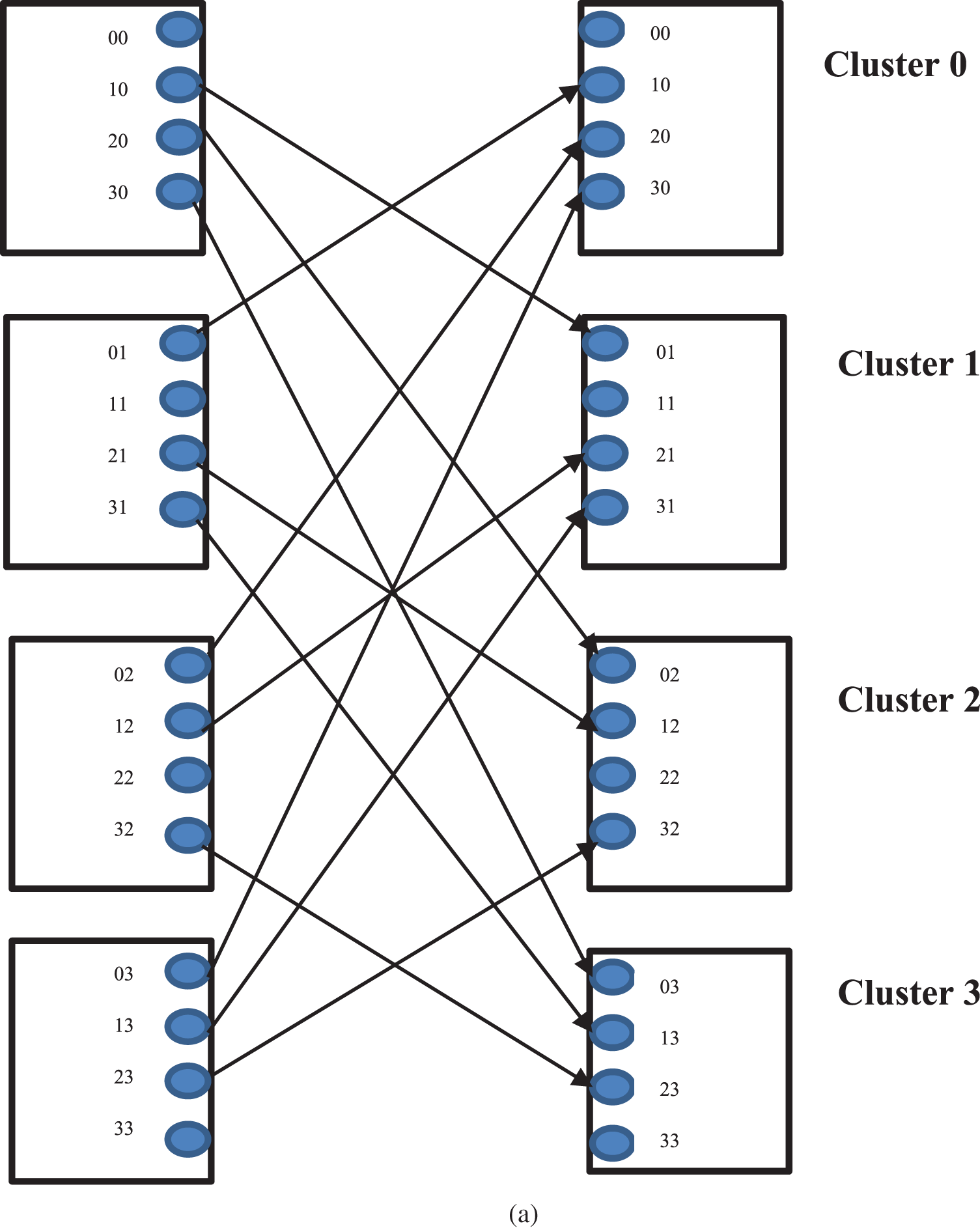
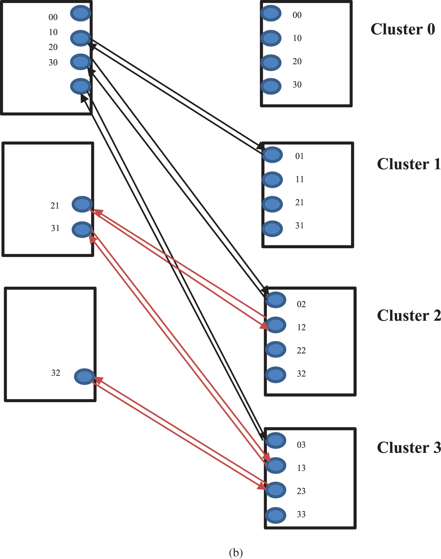
Figure 1: (a) The 4-conjugate shuffle. (b) The equivalent bidirectional connection 4-conjugate shuffle
It can be easily noted that the buses coming out from the same cluster do not cross each other. By aligning the opposite bus with these buses, it can be obtained a group of buses that do not cross each other. As can be seen in Fig. 1b, 12 buses can be put in two groups, i.e., they can be accommodated in two layers of the chip.
The MPCAM organization and the MPCAM-based multi-core system were presented in papers [1,2]. As shown in Fig. 2, the MPCAM is organized as an array of Dual Port Content Addressable Memory modules (DPCAMs) distributed and embedded on the cross points of the multi-core interconnection. The two ports of the DPCAM module allow concurrent read/write operations from the two ports as long as they do not access the same memory location. Through the input port, the Store Back (SB) unit of the core pipeline writes the data and its tag to the least recently written memory line. Through the output port, the Operand Fetch (OF) unit of the core pipeline applies the tag of the required data so that the DPCAM searches for the data in all memory lines simultaneously and reads it if found. In the MPCAM organization, DPCAM modules are connected to the horizontal buses for SB cores, each in its row, and are connected to the vertical buses for OF cores, each in its column, allowing the shared cache to be accessed by any core simultaneously without blocking. It also reduces the access latency which becomes equal to that of the local cache.
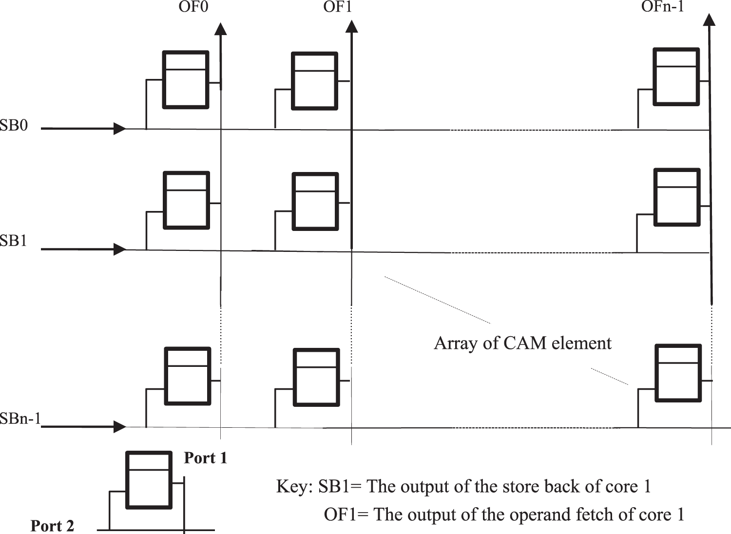
Figure 2: The organization of the MPCAM
3.3 The MPCAM-Based Multi-Core System
In the MPCAM-based multi-core system, if n cores are used, then the MPCAM must have n horizontal buses, n vertical buses, and n2 DPCAM modules; n modules in each row and n modules in each column. The SB units of the core pipelines are connected to the row busses and the OF units are connected to the vertical buses. Through the horizontal bus, the SB unit can write the data and its tag to all DPCAMs in the row. This means that each column will have a copy of the data. So, the OF unit of the core can search for and read the data through the vertical bus of its column. Fig. 3 shows an MPCAM-based multi-core organization. This organization achieves simultaneous access to the shared cache and eliminated the need for router devices between cores inside the same multi-core cluster. This result was fully presented and explored in the article [3].
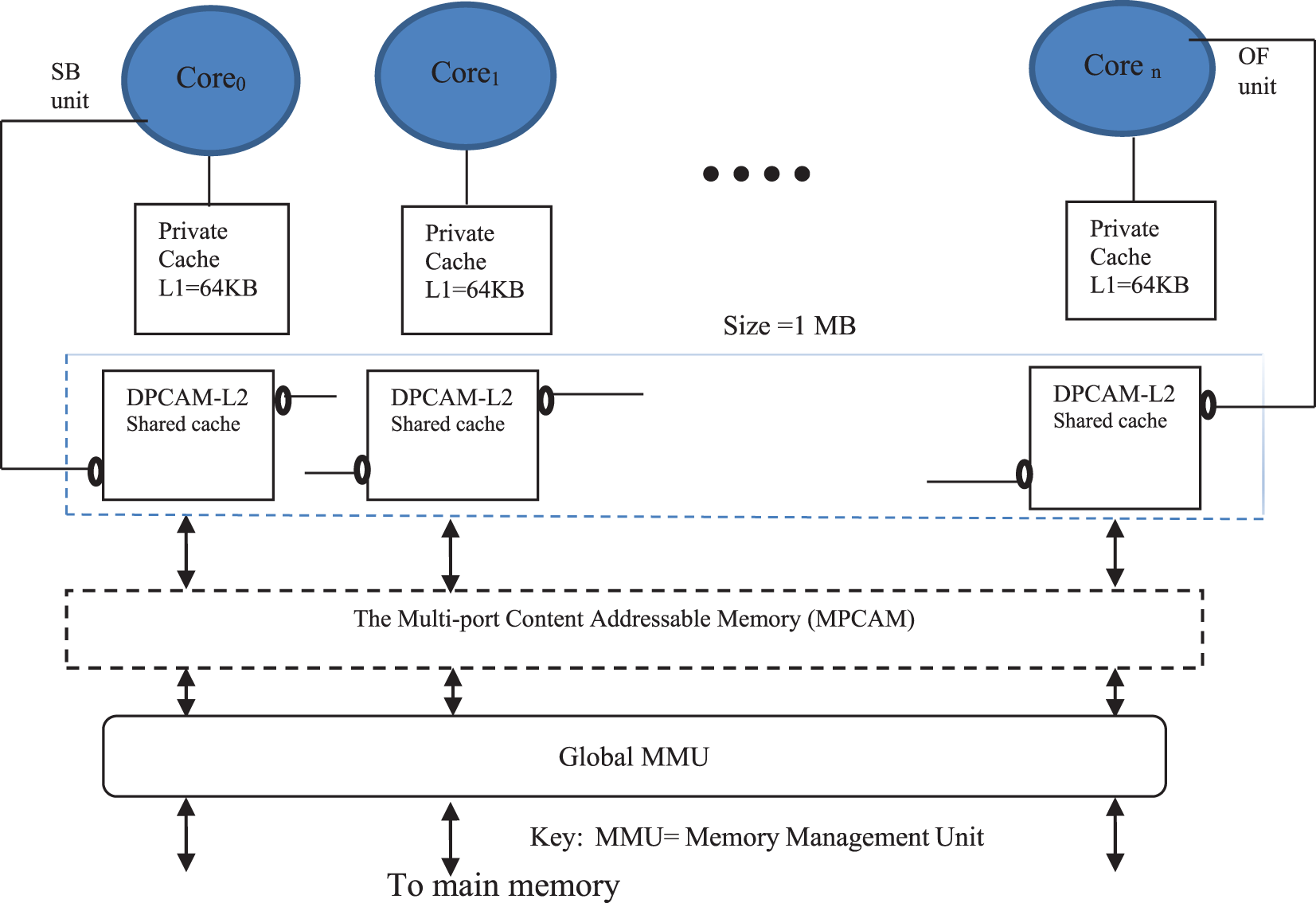
Figure 3: The MPCAM-based multi-core cluster
4 The NCSC Interconnection Scheme
An efficient many-core system can be created if an efficient and simple interconnection scheme is provided and that’s why the NCSC scheme has been chosen for the MPCAM-based clusters. The NCSC uses N-conjugate shuffle combinations to connect between cores of the N system clusters. It is a simple connection method that removes most of the system contention on the inter-cluster level and it is easy to program.
Fig. 4 shows how a bidirectional link (two buses) of the conjugate shuffle connects the OF units of two cores in two different clusters of the many-core system. The switches shown in Fig. 4 guarantee that only one core can access a column of the shared cache of the cluster, regardless of to which cluster this core belongs.
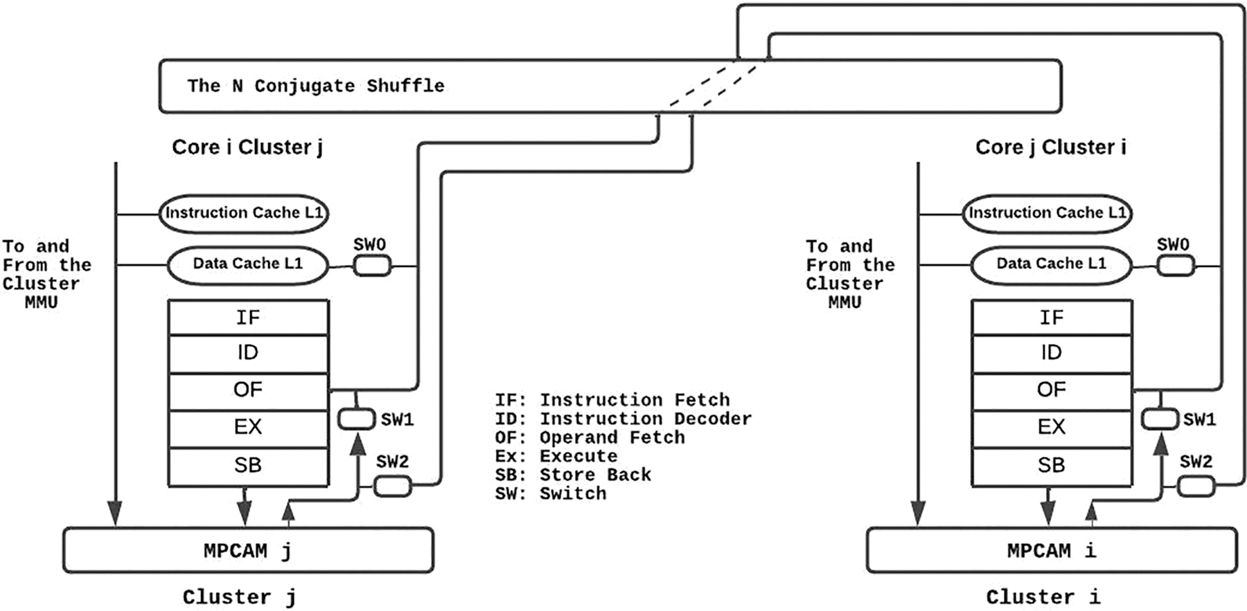
Figure 4: Connecting two cores of two different clusters via the conjugate shuffle
Three bits of the address or the tag would be good enough to control these switches. The only competition occurs when the OF unit of core i in cluster j (OFji) tries to access column j in cluster i while the OFij is trying to access the same column of the MPCAMi in its cluster. The same occurs if OFij tries to fetch data from column i in MPCAMj of cluster j while OFji is trying to access the same column in its cluster (cluster j). In this case, the request coming from within the cluster is given a higher priority, and the request coming from another cluster has to wait for an extra clock cycle. This allows extra time for the core to write the shared data to broadcast the variable to all modules in its row of the MPCAM.
It should be noted that as the core writes the shared data to all modules in its Row, each column of the MPCAM is going to have a copy of this variable. So, any core and its conjugate can access it regardless of which core has produced it.
Let us consider various scenarios in which a path is to be constructed from the source core to the destination as shown in Fig. 5. In scenario 1, assume that core OF00 in cluster 0 wants to access core OF03 in the same cluster and core OF23 in cluster 2 access/read core OF31 in cluster 3 simultaneously. Because the source and destination cores are in the same cluster, the communication process is as follows: OF00 searches the local MPCAM0 and then accesses core 03 data if it was produced formerly.
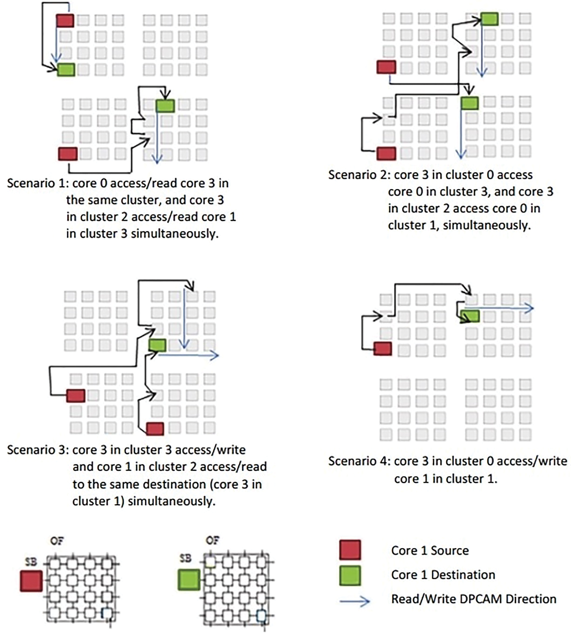
Figure 5: Examples of cores communication
If OF23 doesn’t find the data in local MPCAM2, it recognizes that the data does not belong to this cluster and communicates directly with the OF32, which is the conjugate of OF23 through the NCSC to access internal MPCAM3. In the next cycle, SB32 sends the data to be stored directly to SB23 on MPCAM2. The same happens in scenario 2 but with different addresses of source and destination.
In scenario 3, let’s assume that core SB33 in cluster 3 and OF21 in cluster 2 want to access the same destination core 13, core 3 in cluster 1. This means that SB33 wants to write and OF21 wants to read to/from the same destination simultaneously. Since the source and destination are located in different clusters, SB33 uses SB31 which is the conjugate of SB13. By simple mechanism, SB31 recognizes that the data does not belong to this cluster and communicates directly with SB13 through the NCSC to internally send the data to be stored on MPCAM1. At the same time, OF21 searches the local MPCAM2 and if not found, it will search in the destination cluster. Because OF21 is the conjugate of OF12, they are directly connected through the NCSC to access internal MPCAM2. In the next cycle, SB12 sends the data to be stored directly to SB21 on MPCAM2. In this case, both two sources can be read and stored to/from the same destination without any delay or deflecting the path. Scenario 4 is another example of communication where the source and destination cores are on different clusters
It can be noted that this simple scheme accomplishes the goals of avoiding the complexity of router devices and solving the simultaneous access problem to the same shared memory. Further, the latency (access time) of the shared data is improved as will be explained in the next section.
NCSC and MPCAM have been implemented, compiled, and verified in a many-core system using Quartus Prime 20.1 which includes the Intel-supported ModelSim package and Nios II Embedded Design Suite (EDS) for design and simulation [24]. NCSC was designed using the Cyclone IV-E Field Programmable Gate Array (FPGA) device family, which has new attractive features, especially the number of input/output pins and power consumption [25]. Sixteen cores were used to evaluate the access latency with four cores in each cluster. Both schematic files and Verilog Hardware Description Language (Verilog HDL) code have been used to implement the NCSC in a multi-cluster system. ModelSim and Vector Waveform File (VWF) were used to verify and debug the files in both functional and timing simulations.
The test bench is written using Verilog HDL code that covers all possible access scenarios between cores whether they belong to the same cluster or different clusters. Running the simulator several times shows that the functionality of the NCSC interconnection network based on multi-cluster architecture has been successfully achieved using functional simulation.
In addition to functional simulation, the test bench has also been used to evaluate NCSC access latency. Both functional simulation and access latency are classified into three scenarios. In the first scenario, different cores issued multiple simultaneous writes and read operations for data in the same cluster. In the second scenario, the read and write operations were for data in different clusters. In the third scenario, simultaneous read and write operations in different clusters were made to the same core. The test bench is described in Fig. 6. in detail.
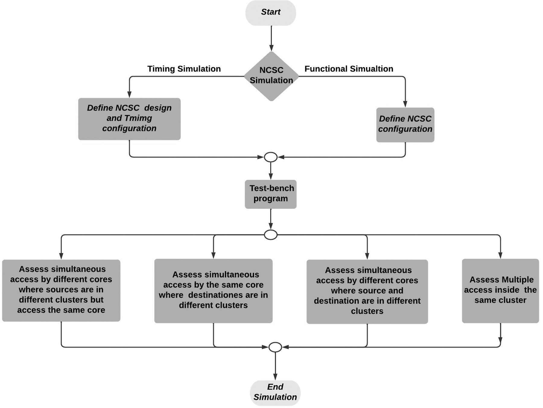
Figure 6: Test benchmark program
Fig. 7 depicts an image of various intervals in the functional simulation of NCSC, the clock period is set to 10 ns for reading and writing. In the first interval (0 to 10 ns), both core 11 in the first cluster and core22 in the second cluster broadcast their shared data with tag source (tags) (A1) and (10C1) respectively. In the second interval (10 to 20 ns), core OF31 in the first cluster read shared data produced by core11 in the same cluster, and core OF44 in the fourth cluster read shared data produced by core22 from another cluster (in the second cluster) simultaneously. In the OF31, because the source and destination cores are in the same cluster, the communication process is followed using the MPCAM1 organization within the local cluster. Whereas OF44 does not belong to the same cluster that has core22, the wanted shared data will not be found in the local cluster. So, by comparing the tags. OF44 communicates directly using the OF24 which is the conjugate of the second cluster through the NCSC to read internal MPCAM2. In this interval, the wanted shared data appeared on the Dout-core31 and Dout-core44 correctly. In the third Interval (20 to 30 ns), various cores from different clusters can read and write simultaneously, where core11 in the first cluster writes its shared data with tags (A7), core OF23 in the third cluster read shared data with tags (A1) produced by another cluster (in the first cluster), and core OF44 in the fourth cluster read shared data with tags (A1) produced from a different cluster (the first cluster) simultaneously. In this scenario, core11 broadcasts its shared data to MPCAM1 in cluster one, and OF23 and OF 44 use OF13 and OF14 respectively which is the conjugate of these cores to cluster one. The output result appeared on the Dout-core23 and Dout-core44 correctly. Finally, in the fourth interval (30 to 40 ns), core OF44 in the fourth cluster reads shared data with tags (A7) produced by another cluster (in the first cluster). Here, OF44 uses OF14 which is the conjugate of cluster one in the NCSC interconnection network. The output result appeared on the output bus Dout-core44 correctly.
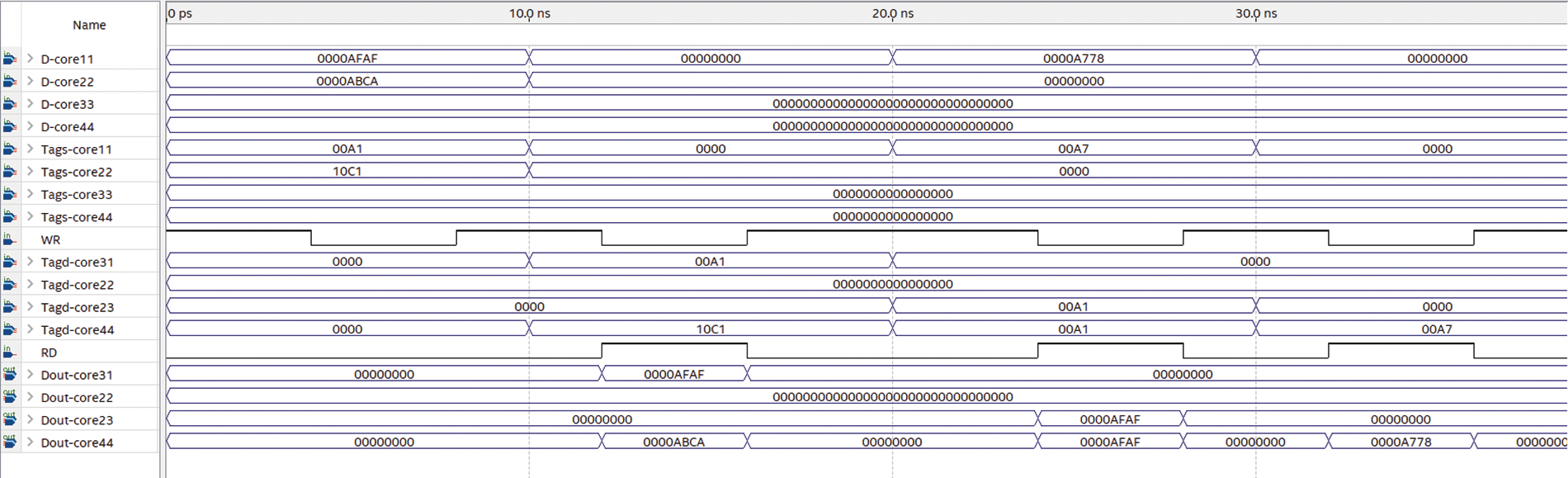
Figure 7: Function simulation for a read operation
Fig. 8 shows an image of several intervals for writing operation over NCSC, a new DI-core pin was added to monitor the writing operation. In the first interval (0 to 10 ns), core21 in the first cluster, core 42 in the second cluster, and core 24 in the fourth cluster write their shared data with tags (0211), (1422), and (3074), respectively, each to its MPCAM. It can be observed that the written data are stored correctly and displayed in DI-core21, DI-core42, and DI-core24. In the second interval (10 to 20 ns), core21, core42, and core 24 write the shared data to these MPCAM simultaneously, each one uses its special tags. The written data appeared on the DI-core21, Dout-core42, and Dout-core24 correctly.
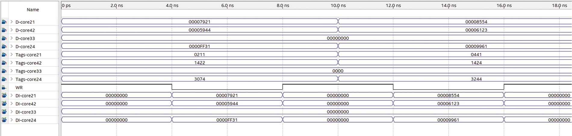
Figure 8: Function simulation for a write operation
In the functional simulation, it can be noticed that written or read data appear on the DI-core and Dout-core pins without taking into account the delay produced by design components.
The Timing Analyzer tool is used to evaluate the read/write latency for the MPCAM and NCSC. In this section, all scenarios that were presented in the functional simulation will be assessed in the timing simulation. The timing simulation for read/write operations of the proposed system is shown in Figs. 9–12.
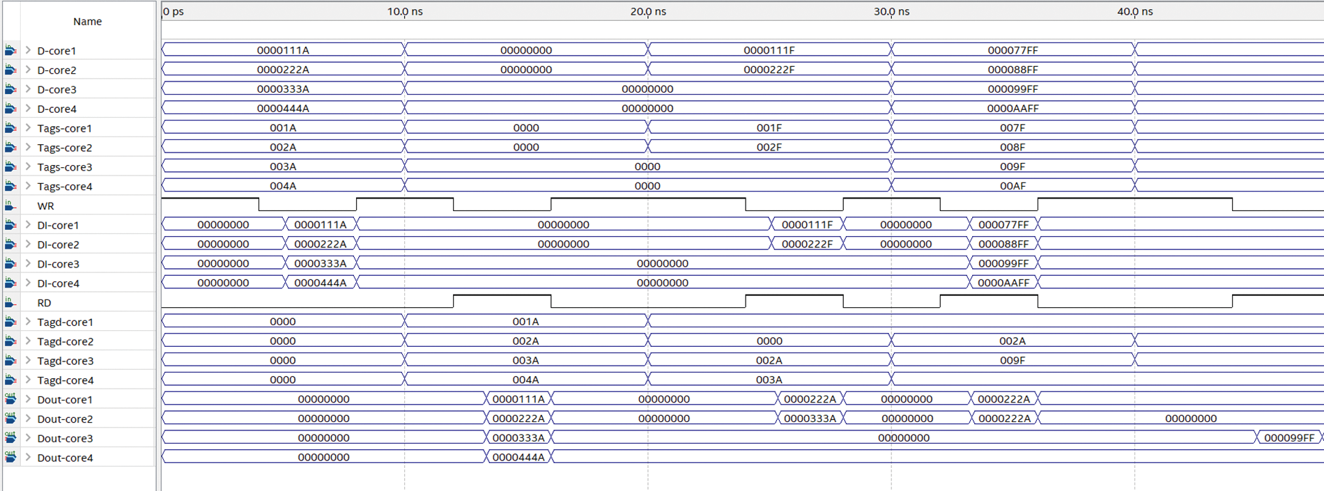
Figure 9: MPCAM organization Timing Simulation 1
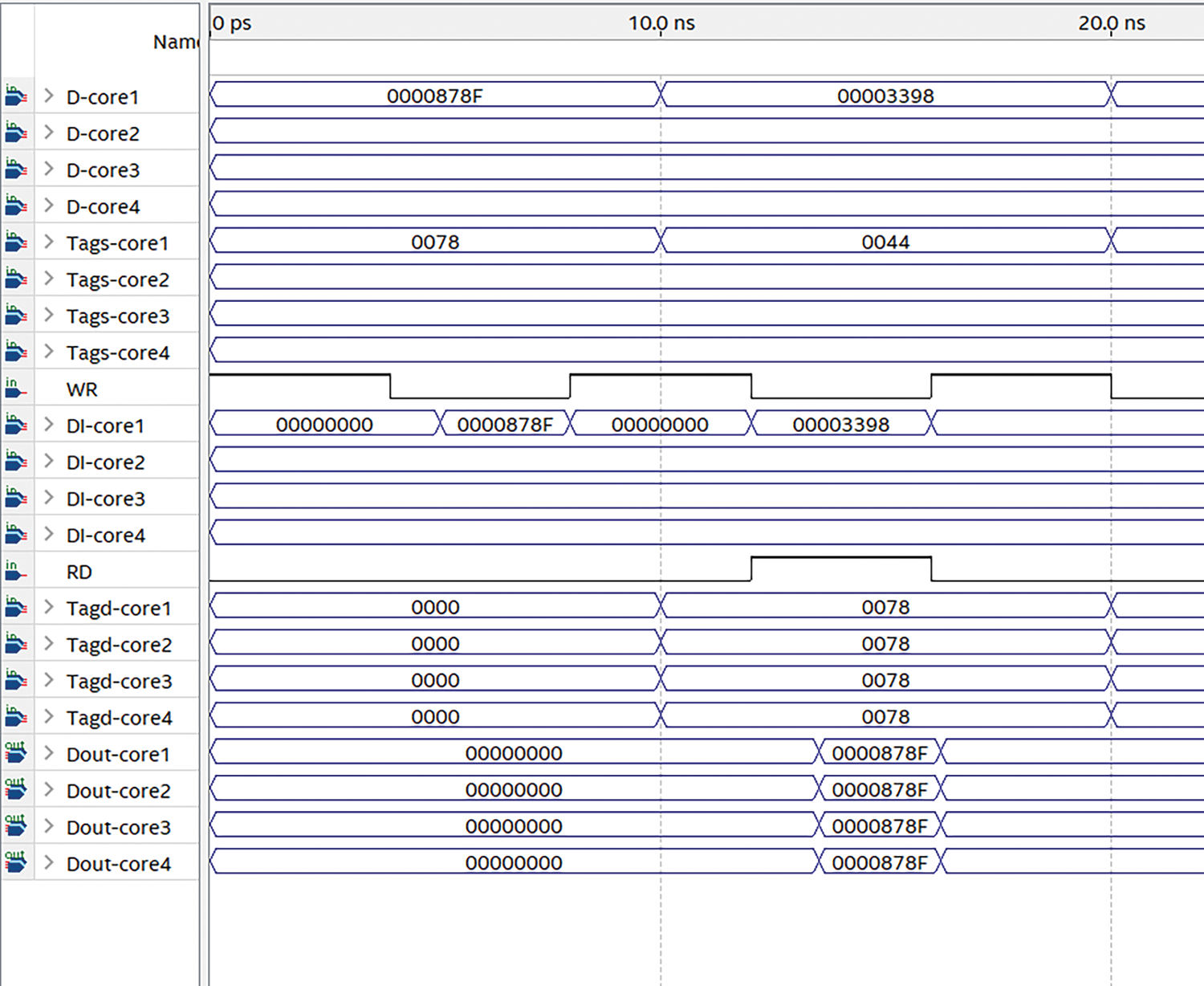
Figure 10: MPCAM organization Timing Simulation 2
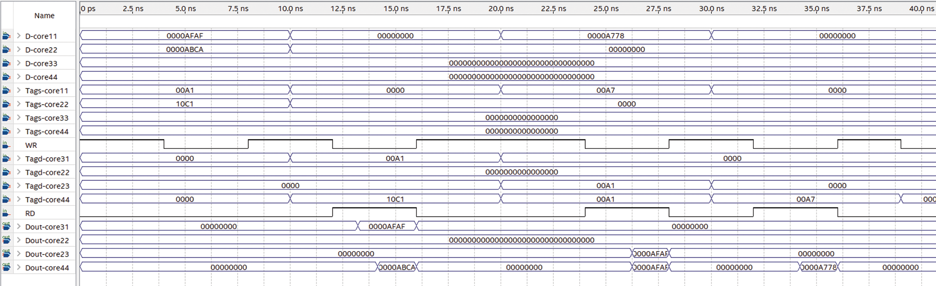
Figure 11: NCSC organization Timing Simulation for a read operation
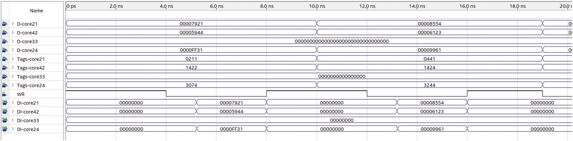
Figure 12: NCSC organization Timing Simulation for a write operation
Fig. 9 shows the timing simulation for MPCAM. In the first interval (0 to 10 ns), all cores simultaneously broadcast their shared data with their special Tags. Instantly the written data (pine DI-core) appears clearly on all modules in its row after a short delay as soon as the WR signal goes down. After running the test bench on the simulator one hundred times, it can be noticed that the average access latency of writing on MPCAM organization is around 1.084115 ± 0.03384 ns. The second (10 to 20 ns) interval shows the latency assessment for a read access. To read data that is already written in all MPCAM modules, the Tage destination (Tagd) (1A, 2A, 3A, and 4A) which is provided by core1, core2, core3, and core4 respectively are simultaneously compared to the tags in all MPCAM modules in the same column. The results appear on output buses (Dout-core) after the delay time. The delay for read operation was calculated using an average of roughly one hundred intervals of test benches, it was noticed that the delay for a read operation is around 1.27804 ± 0.086823 ns. The latencies assessment for concurrent read and write operations to the memory locations are shown in the third (20 to 30 ns) and fourth (40 to 50 ns) periods which was performed around 100 times for each of the two cases. For the scenario when many memory locations are being read and written simultaneously, the latency is 1.1909 ± 0.02363 ns this is almost the same as the separate read operations latency. On the other hand, when write and read operations are performed simultaneously to the same memory locations, the data is written with a latency of 1.3105 ± 0.091955 ns to the destination location, while the read process waits for the following interval then the shared data is read with a total latency 1.2780 ± 0.086823 plus the time of the interval. All these measurements were proved by using Statistical Package for Social Sciences (SPSS) and T-tested with a confidence interval of 95%.
Fig. 10 shows two scenarios of read/write over MPCAM. In the first interval (0 to 10 ns), core 1 broadcasts shared data to all DPCAM models in its row with Tags (0078). Instantly the written data (pine DI-core) appears clearly after a time delay of 1.084115 ± 0.03384 ns as soon as the WR signal goes down this is almost the same as the separate write operations latency. In the second interval (10 to 20 ns), all cores simultaneously read the shared data which was produced by core 1 in the first interval. The results appear on Dout-core pines with a time delay of 1.27804 ± 0.086823 ns, which is almost the same as the separate read operations latency. From the timing simulation, it can be noticed that the write and read operations to the shared cache would not take more than 1.3 ns compared to 5.3 ns at the L2 cache and 19.5 ns in the L3 cache in Nehalem Intel i7. On the other hand, it needs 12 ns at the L2 cache, and 21 ns in the L3 cache in AMD’s Bulldozer family [26].
As a result of this simulation, it was demonstrated that all cores in the MPCAM organization can access shared data simultaneously without contention, blocking, and arbitration issues.
Fig. 11 shows the timing simulation of the proposed NCSC with several intervals. In the first interval (0 to 10 ns), both core 11 and core 22 write their shared data with tags (00A1) and (10C1) respectively. In the second interval (10 to 20 ns), core OF31 read shared data with tags (00A1) from the same cluster, and core OF44 read shared data with tags (10C1) from another cluster simultaneously. In this interval, the read latency between the two cases is different. To read data that is already written in the same cluster, the tagd (00A1) which is provided by core31 is simultaneously compared to the tags in the MPCAM column within cluster one. The results appear on output buses (Dout-core 31) after some delay. The delay for read operation was assessed using an average of roughly one hundred intervals of test benches, it was found that the read process delay within the same cluster is around 1.26226 ± 0.090591 ns. On the other hand, to read data that is already written in another cluster, core44 wants to read data produced by core22. OF44 communicates directly using the OF24 which is the conjugate of the second cluster through the NCSC to read internal MPCAM2. The results appear on output buses (Dout-core 44) after some delay. Using an average of one hundred intervals of test benches, it was noticed that the delay for read access between cores that belong to different clusters is around 1.92738 ± 0.139588. In the third Interval (20 to 30 ns), core11 in the first cluster writes its shared data with tags (00A7), core23 in the third cluster read shared data with tags (00A1) produced by core11, and core OF44 read shared data with tags (00A1) simultaneously. In this interval, core11 broadcast its shared data to MPCAM1 in cluster one, and OF23 and OF44 connect to core 11 in the first cluster using OF13 and OF14 respectively which is the conjugate of these cores to cluster one through the NCSC IN. The results appear on output buses (Dout-core23) after some delay. It was noticed that the delay for read access between cores in different clusters is around 1.92738 ± 0.139588 ns, which is nearly equal to the latency of read operation in (Dout-core44). The third Interval (30 to 40 ns) shows the same behavior as the second interval l (20 to 30 ns).
Fig. 12 shows an image of two intervals to assess the write latency over NCSC. In the first interval (0 to 10 ns), core21, core42, and core24 write their shared data with their tags (0211), (1422), and (3074) respectively, each to its MPCAM. It can be observed that the written data are stored in DI-core21, DI-core42, and DI-core24 pins after a delay time with an average of 1.14785 ± 0.04532 which is almost the same as the separate write operations latency in the MPCAM organization. In the second interval (10 to 20 ns), core21, core42, and core24 write the shared data to their MPCAM simultaneously with an average delay of 1.15235 ± 0.06132 which is identical to the latency in the previous interval.
5.3 Area and Power Consumption Analysis
Cache memories and routers on any NoC topology are the dominant factors in area and power consumption. Unfortunately, NoC consumes a lot of power, increasing the chip’s total power consumption. Research has already verified that NoC consumes about 40% of the chip’s power without counting the cache power consumption [4]. On the other hand, other studies revealed that routers’ structure in mesh or tour topology consumes about 28% of the total power and 17% of the total area in the Intel chip [17], and also adds additional latency due to increased hardware structures that negatively affect the performance. Therefore, since routers are the most power-consuming components of the interconnect network, this paper proposed the NCSC interconnection scheme that eleminates the need for router devices and enhances both area and power overheads. Furthermore, NoC with appropriate power consumption plays a leading role in increasing scalability in many-core systems.
As a future work, a Power analysis simulator can be used to estimate power and area overhead for NCSC which was used for this purpose in MPCAM [1,3].
In on-chip many-core systems, the NoC topologies have been considered to be the best; however, they have some disadvantages like high scalability cost, power, latency, and contention during access to shared cache, which is mostly due to the usage of router-based structures. Therefore, researchers try to find alternatives for these topologies based on router-less interconnection. In this paper, a scalable topology of the many-core processor systems called NCSC was presented. The proposed topology has additional features such as high scalability, fixed latency on the intra-cluster and inter-cluster levels, and elimination of routers and arbiters which solves the problem of simultaneous access to the shared cache.
NCSC has been implemented using the Cyclone IV-E FPGA device family. After running the test bench program several times it was found that the main functions of NCSC organization in terms of reading, writing, and simultaneous read-write are accomplished inside and between clusters. The latency of reading and writing by multiple cores within the cluster and between clusters has been assessed. NCSC provides non-blocking access between cores with average latency for write access within the same cluster is around 1.14785 ± 0.04532 ns which is almost the same as the separate write operation in MPCAM, the average read latency within the same cluster is 1.26226 ± 0.090591 ns and the latency for read access between cores from different clusters is around 1.92738 ± 0.139588 ns. On the other hand, the simulation result shows that competition happens only if simultaneous access comes from the same cluster and a request comes from another to the same column in MPCAM. In this case, access coming from the same cluster is given a higher priority, whereas the request coming from another cluster has to wait until the next clock cycle. So, the read latency becomes 1.92738 ± 0.139588 ns pulse the delay from the competition.
The realization of the MPCAM-based multi-core cluster and conjugate shuffle network in many-core systems opens the door wide for massively parallel processing on a chip and makes life easier for chip designers and programmers.
In future work, more research can be conducted on the NCSC topology. Other crucial dynamic performance metrics like throughput, latency overhead, area, and power consumption can be evaluated. In addition, all components of this topology, including core interfaces, can be built to ensure the authenticity of NCSC within a many-core system. After that, it can be implemented in Verilog and verified and synthesized using some design tools.
Acknowledgement: We would like to thank Prof. Adil Amirjanov for his valuable advice and continuous support. We would also like to acknowledge the advice and support from the Department of Computer System Engineering, Arab American University.
Funding Statement: The authors received no specific funding for this study.
Author Contributions: The authors confirm their contribution to the paper as follows: study conception and related work: Allam Abumwais and Mujahed Eleyat; data analysis: Allam Abumwais; the components of the proposed system: Allam Abumwais; performance analysis: Allam Abumwais and Mujahed Eleyat; draft manuscript preparation: Mujahed Eleyat. All authors reviewed the results and approved the final version of the manuscript.
Availability of Data and Materials: Available upon request.
Conflicts of Interest: The authors declare that they have no conflicts of interest to report regarding the present study.
References
1. A. Abumwais, A. Amirjanov, K. Uyar1 and M. Eleyat, “Dual-port content addressable memory for cache memory applications,” Computer, Material & Continua, vol. 3, no. 70, pp. 4583–4597, 2021. [Google Scholar]
2. A. Abumwais and A. Ayyad, “The MPCAM based multi-core processor architecture: A contention free architecture,” Wseas Transactions on Electronics, vol. 9, no. 13, pp. 105–111, 2018. [Google Scholar]
3. A. Abumwais and M. Obaid, “Shared cache based on content addressable memory in a multi-core architecture,” Computers, Materials & Continua, vol. 74, no. 3, pp. 4952–4963, 2022. [Google Scholar]
4. J. Hennessy and D. Patterson, Computer Organization and Design: The Hardware Software Interface. 2nd ed., Cambridge, MA, United States: Elsevier, pp. 520–580, 2020. [Google Scholar]
5. A. Singh, M. Shafique, A. Kumar and J. Henkel, “Mapping on multi/many-core systems: Survey of current and emerging trends,” in 50th ACM/EDAC/IEEE Design Automation Conf., (DAC), Austin, TX, USA, pp. 1–10, 2013. [Google Scholar]
6. A. N. Udipi, N. Muralimanohar and R. Balasubramonian, “Towards scalable, energy-efficient, bus based on-chip networks,” in HPCA-16 2010 the Sixteenth Int. Symp. on High-Performance Computer Architecture, Bangalore, India, pp. 1–12, 2010. [Google Scholar]
7. S. R. Vangal, J. Howard, G. Ruhl, S. Dighe, H. Wilson et al., “An 80-tile sub-100-w teraflops processor in 65-nm CMOS,” IEEE Journal of Solid-State Circuits, vol. 43, no. 1, pp. 29–41, 2008. [Google Scholar]
8. Z. Zhang, D. Refauvelet, A. Greiner, M. Benabdenbi and F. Pecheux, “On-the-field test and configuration infrastructure for 2-D-mesh NoCs in shared-memory many-core architectures,” IEEE Transactions on Very Large Scale Integration (VLSI) Systems, vol. 22, no. 6, pp. 1364–1376, 2013. [Google Scholar]
9. C. A. Guzman, Y. Cho and B. Egger, “SnuMAP: An open-source trace profiler for manycore systems,” in European Network on High Performance and Embedded Architecture and Compilation (HiPEAC), Stockholm, Sweden, pp. 1–13, 2017. [Google Scholar]
10. S. Liu, S. Liu, Y. Cheng and L. Yu, “Hybrid network-on-chip: An application-aware framework for big data,” Complexity, vol. 2018, pp. 1–11, 2018. [Google Scholar]
11. Y. He, J. Jiao, T. Cao and M. Kondo, “Energy-efficient on-chip networks through profiled hybrid switching,” in Proc. of the 2020 on Great Lakes Symp. on VLSI, Beijing, China, pp. 241–246, 2020. [Google Scholar]
12. Y. Hoskote, S. Vangal, A. Singh, N. Borkar and S. Borkar, “A 5-GHz mesh interconnect for a teraflops processor,” IEEE Micro, vol. 27, no. 5, pp. 51–61, 2007. [Google Scholar]
13. M. R. Awal, M. M. H. Rahman, R. M. Nor, T. Sembok and M. A. H. Akhand, “Architecture and network-on-chip implementation of a new hierarchical interconnection network,” Journal of Circuits, Systems and Computers, vol. 24, no. 2, pp. 1–21, 2015. [Google Scholar]
14. W. Li, B. Guo, X. Li, S. Yin, Y. Zhou et al., “Nesting ring architecture of multichip optical network on chip for many-core processor systems,” Optical Engineering, vol. 56, no. 3, pp. 35096–35106, 2017. [Google Scholar]
15. W. Li, B. Guo, X. Li, Y. Zhou, S. Huang et al., “A large-scale nesting ring multi-chip architecture for manycore processor systems,” Optical Switching and Networking, vol. 31, no. 1, pp. 183–192, 2019. [Google Scholar]
16. S. Liu, T. Chen, L. Li, X. Feng, Z. Xu et al., “IMR: High-performance low-cost multi-ring nocs,” IEEE Transactions on Parallel and Distributed Systems, vol. 27, no. 6, pp. 1700–1712, 2015. [Google Scholar]
17. F. Alazemi, A. AziziMazreah, B. Bose and L. Chen, “Routerless networks-on-chip,” in IEEE Int. Symp. on High Performance Computer Architecture (HPCA), Vienna, Austria, pp. 492–503, 2018. [Google Scholar]
18. B. Bohnenstiehl, A. Stillmaker, J. Pimentel, T. Andreas, B. Liu et al., “A 5.8 pJ/Op 115 billion ops/sec, to 1.78 trillion ops/sec 32 nm 1000-processor array,” in Symp. on VLSI Circuits (VLSI-Circuits), Honolulu, HI, USA, pp. 1–2, 2016. [Google Scholar]
19. T. Lin, D. Penney, M. Pedram and L. Chen, “A deep reinforcement learning framework for architectural exploration: A routerless NoC case study,” in 2020 IEEE Int. Symp. on High Performance Computer Architecture (HPCA), San Diego, CA, USA, pp. 99–110, 2020. [Google Scholar]
20. T. Lin, D. Penney, M. Pedram and L. Chen, “Optimizing routerless network-on-chip designs: An innovative learning-based framework,” arXiv preprint arXiv:1905.04423, 2019. [Google Scholar]
21. M. Abd-El-Barr and T. F. Al-Somani, “Topological properties of hierarchical interconnection networks: A review and comparison,” Journal of Electrical and Computer Engineering, vol. 2011, pp. 1–12, 2011. [Google Scholar]
22. G. Khanna, R. Mishra and S. K. Chaturvedi, “Design of fault tolerant shuffle exchange gamma interconnection network layouts,” Journal of Interconnection Networks, vol. 17, no. 2, pp. 1750005-1–1750005-18, 2017. [Google Scholar]
23. H. Lahdhiri, J. Lorandel, S. Monteleone, E. Bourdel and M. Palesi, “Framework for design exploration and performance analysis of RF-NoC manycore architecture,” Journal of Low Power Electronics and Applications, vol. 10, no. 4, pp. 1–15, 2020. [Google Scholar]
24. I. Corporation, “Intel® quartus® prime Pro edition user guide, timing analyzer tool,” 2021. [Google Scholar]
25. I. Marouf, M. M. Asad, A. Bakhuraibah and Q. Abu Al-Haija, “Cost analysis study of variable parallel prefix adders using altera cyclone IV FPGA kit,” in 2017 Int. Conf. on Electrical and Computing Technologies and Applications (ICECTA), Ras Al Khaimah, United Arab Emirates, pp. 1–4, 2017. [Google Scholar]
26. J. Hruska, “How L1 and L2 CPU caches work, and Why they’re an essential part of modern chips,” Extremetech, vol. 1, pp. 1–6, 2018. [Google Scholar]
Cite This Article
 Copyright © 2023 The Author(s). Published by Tech Science Press.
This work is licensed under a Creative Commons Attribution 4.0 International License , which permits unrestricted use, distribution, and reproduction in any medium, provided the original work is properly cited.
 Downloads
 Citation Tools