
 Submit a Paper
 Propose a Special lssue
 Open Access
ARTICLE
Atomistic Insights into Aluminium–Boron Nitride Nanolayered Interconnects for High-Performance VLSI Systems
1 Department of Electronics and Communication Engineering, Dayananda Sagar Academy of Technology and Management, Bengaluru, 560082, India
2 School of Electronics Engineering, Vellore Institute of Technology University, Vellore, 632014, India
* Corresponding Author: Mandar Jatkar. Email:
Computers, Materials & Continua 2026, 86(3), 23 https://doi.org/10.32604/cmc.2025.072507
Received 28 August 2025; Accepted 19 November 2025; Issue published 12 January 2026
 View Full Text
 Download PDF
Abstract
As circuit feature sizes approach the nanoscale, traditional Copper (Cu) interconnects face significant hurdles posed by rising resistance-capacitance (RC) delay, electromigration, and high power dissipation. These limitations impose constraints on the scalability and reliability of future semiconductor technologies. Our paper describes the new Vertical multilayer Aluminium Boron Nitride Nanoribbon (AlBN) interconnect structure, integrated with Density functional theory (DFT) using first-principles calculations. This study explores AlBN-based nanostructures with doping of 1Cu, 2Cu, 1Fe (Iron), and 2Fe for the application of Very Large Scale Integration (VLSI) interconnects. The AlBN structure utilized the advantages of vertical multilayer interconnects to both reduce the RC delay while enhancing signal integrity. Key parameters like Fermi energy, bandgap, binding energy, conduction channels, quantum resistance, and RC delay were analyzed. Through modeling and large-scale simulation, the structural, electronic, and stability attributes of the AlBN interconnects are analyzed, and the results illustrate considerable improvements in signal propagation against Cu interconnect structures. These findings confirm the tunable, high-performance nature of AlBN-2Fe, making it a promising candidate for future high-speed, low-power VLSI interconnect technologies. We demonstrated an advanced energy-efficient interconnect that can be easily scaled for future nanoscale VLSI circuit design and gives rise to a next generation of viable interconnect technology for high-capacity, high-speed, reliable semiconductor technology.Keywords
The performance of contemporary electronic systems has been greatly improved by the ongoing downsizing of semiconductor devices and the quick development of VLSI technology. However, increased signal propagation delay, high resistivity, high power consumption, and electromigration problems are some of the significant nanoscale obstacles that conventional Cu interconnects must overcome. These limitations hinder the performance and reliability of high-speed, low-power circuits used in modern computing, communication, and artificial intelligence applications [1,2]. Copper has been the dominant interconnect material in semiconductor technology due to its relatively low resistivity and high conductivity. However, as transistor sizes approach the sub-7 nm node, Cu interconnects exhibit increasing resistance-capacitance (RC) delays due to factors such as surface scattering, grain boundary effects, and electron mean free path limitations [3]. Carbon-based nanomaterials such as carbon nanotubes and nanoribbons have emerged as potential replacements due to their superior electrical and thermal properties [4,5]. However, due to electron hopping between layers, horizontal interconnects have resistance and decreased carrier mobilities. Their overall performance is also affected by contact resistance, particularly at the metal interface level, where fabrication problems can arise. The integration of these materials helps stabilize charge transport, reduce leakage currents, and improve performance scalability for future semiconductor nodes [6]. As semiconductor technology advances toward nanoscale VLSI circuits, traditional Cu interconnects face severe challenges such as high resistivity, RC delay, electromigration, and thermal instability, leading to degraded signal transmission, power efficiency, and reliability. As operational frequencies increase, parasitic effects and Joule heating further limit Cu’s performance, making efficient thermal management difficult. A summary of recent advancements in Aluminium (Al)-based interconnects has been added to provide better context. Recent studies highlight improved electromigration resistance, lower cost, and compatibility with Complementary Metal Oxide Semiconductor (CMOS) processes. These developments justify exploring Al-based interconnects as potential alternatives to copper for advanced VLSI systems [7–9]. The demand for faster, energy-efficient, and reliable semiconductor devices has surged with advancements in Artificial Intelligence (AI), Internet of Things (IoT), high-speed computing, and 5G. New materials are needed for interconnects that are high-speed, thermally stable, and low-power, because traditional Cu interconnects have physical and electrical limitations. Because of graphene’s extraordinary heat conductivity and exceptionally high electron mobility, Cu has the potential to replace graphene. These interconnects provide high-speed charge transport and low RC delay, but horizontal interconnects have obstacles in electron hopping and impedance mismatches. The scaling of Very Large-Scale Integration circuits has highlighted the drawbacks associated with conventional Cu interconnects, including high resistivity, electromigration, and increasing RC latency at nanoscale dimensions [10]. As a result of these disadvantages, researchers have investigated alternative materials as a remedy, such as carbon-based nanostructures, such as carbon nanotubes (CNTs) and graphene nanoribbons (GNRs), because they are believed to have greater electrical and thermal properties [11–14]. Nanoscale VLSI circuits that combine Aluminium-boron-nitride (AlBN) interconnects with high-K dielectric materials (H-KDM) represent an alternative to conventional copper interconnects. Studies of AlBN interconnects with H-KDM showed that AlBN has unique material properties, including high dielectric strength and excellent thermal resistance, which together enhance signal integrity, reduce RC timing delays, and improve power efficiency. In order to solve the shortcomings of Horizontal Multilayer Interconnect (HMI), researchers have proposed Vertical Multilayer Interconnect (VMI), enabling better charge transport, reduced resistance, and improved performance. Studies have shown that VMI’s outperform Cu and HMI’s in terms of signal integrity, propagation delay, and power efficiency [15,16]. The integration of High-K Dielectric Materials has been explored to enhance the performance of interconnects. High-K materials reduce impedance mismatches, improve charge transport, and minimize signal losses, making them suitable for next-generation high-speed interconnects [17,18]. Recent studies have explored novel nanoribbon-based interconnects using first-principles methods. GaN, antimonene, and doped GeS nanoribbons have shown promising electrical and structural properties for high-speed nanoscale interconnect applications [19–21]. These Non-Equilibrium Green’s Function (NEGF) analysis highlights their potential as next-generation materials for nanoelectronics [22–24]. Research indicates that embedding H-KDM AlBN structures significantly improves electron mobility, reduces power dissipation, and enhances scalability. Comparative studies confirm that AlBN with H-KDM outperforms Cu, CNT, and GNR interconnects in terms of delay, bandwidth, and thermal stability, making it a strong candidate for future nanoscale VLSI applications.
In this work, First-principles calculations were performed under the density DFT framework in the Quantum Atomistix ToolKit (ATK) software. For the exchange–correlation interaction description, the local density approximation (LDA) functional was utilized. The Kohn–Sham wave functions were expressed in a plane-wave basis set with a kinetic energy cutoff of 100 Ry, chosen from interatomic force and total energy convergence tests. Vacuum spacing was added, 10 Å, perpendicular to the plane of the nanoribbon. It avoids spurious periodic image interactions in the non-periodic direction. Brillouin zone (BZ) sampling was carried out using a Monkhorst–Pack k-point mesh of 1 × 1 × 100 for geometry optimization according to the periodicity of the nanoribbon. The structural optimization includes van der Waals (vdW) interactions to accurately capture interlayer and surface adhesion effects. Incorporating vdW forces ensures reliable estimation of equilibrium geometries and binding energies in the optimized structure. All atomic positions were relaxed until the force on each atom was less than 0.01 eV/Å, and the total energy convergence threshold was set to 10−6 eV. For structural modeling, AlBN structures were constructed using a rectangular supercell with periodic boundary conditions along the ribbon axis. The total energy was minimized with respect to the lattice parameter along this axis to obtain the equilibrium ribbon geometry. All computed electronic band structures and density of states (DOS) were post-processed using the built-in Quantum Atomistic (ATK) Simulation Software tool.
The performance of the proposed AlBN interconnects with High-K Dielectric Materials is evaluated through computational modeling and simulations. Various parameters such as resistance, capacitance, propagation delay, and power dissipation are analyzed. The obtained results demonstrate the superior electronic and thermal performance of AlBNs, making them a promising alternative for next-generation VLSI circuits. The following sections present a detailed analysis of the key findings, including the impact of high-k materials, structural variations, electronic properties, stability analysis, and interconnect modelling.
The study of the band structure showed that AlBNs exhibit a narrow bandgap, which enhances their metallic behavior and charge carrier mobility. Unlike horizontal multilayer nanoribbons, which suffer from electron hopping between layers, the vertical configuration reduces interlayer resistance and allows for efficient ballistic electron transport. The band structures of the layers taken are represented below for AlBN doped with Cu and Fe atoms.
The electronic band structures of AlBN doped with Cu and Fe atoms are shown in Figs. 1 and 2, respectively. The left and right panels correspond to systems doped with one and two metal atoms. For Cu-doped AlBN (Fig. 1), the overall band dispersion shows a reduction in the band gap compared to pristine AlBN, indicating enhanced electronic conductivity upon Cu incorporation. In the single-atom doped case, the Fermi level shifts slightly toward the conduction band, suggesting n-type doping behavior due to the Cu contribution of additional electrons. With two Cu atoms, additional impurity states emerge near the Fermi level, further narrowing the band gap and enabling continuous electronic states across the Fermi energy, a sign of metallic character. This indicates that higher Cu concentration improves the carrier transport capability of the AlBN framework, beneficial for interconnect applications. For Fe-doped AlBN (Fig. 2), Similar to Cu doping, Fe incorporation leads to the appearance of impurity bands near the Fermi level. However, the Fe-doped system shows a slightly larger density of states around the Fermi energy, suggesting stronger hybridization between Fe-3d and N-2p orbitals. The overlap of valence and conduction bands for two Fe atoms indicates a metallic or semi-metallic transition, which enhances electrical conductivity. The stronger interaction and higher cohesive energy of Fe may also contribute to better structural stability under operational stress. Overall, both dopants induce band gap narrowing and metallic transition, but Fe doping exhibits slightly stronger electronic coupling and band dispersion near the Fermi level, implying improved charge transport and structural robustness compared to Cu doping.
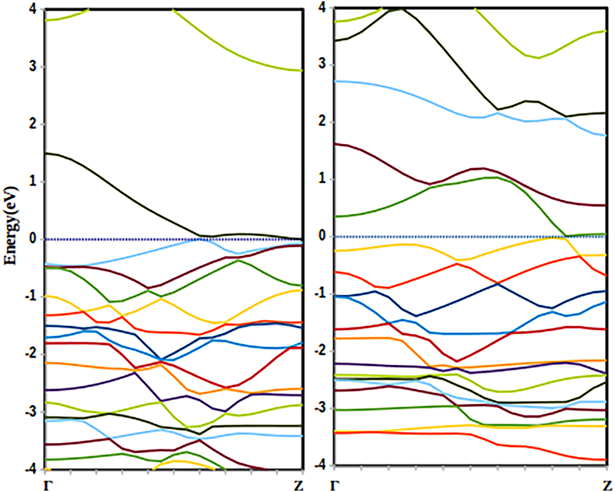
Figure 1: Band structure of AlBN with doped Cu atoms [1 atom (left) & 2 atoms (right)]
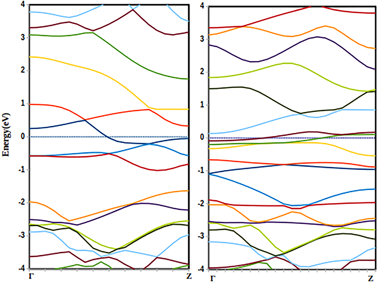
Figure 2: Band structure of AlBN with doped Fe atoms [1 atom (left) & 2 atoms (right)]
Table 1 refers to the band gap analysis of AlBN-doped structures. The electronic band structure of pristine AlBN (Fig. 3) exhibits a distinct separation between the valence and conduction bands, indicating its semiconducting nature with a band gap of 2.3 eV. The Fermi level lies within the band gap, confirming the absence of states at the Fermi energy. The calculated band gap, estimated from the energy difference between the valence-band maximum (VBM) and the conduction-band minimum (CBM), is 2.3 eV, which is consistent with the wide-band-gap behavior reported for hexagonal AlBN Pristine nanoribbon. The relatively flat nature of the valence bands near the VBM suggests localized electronic states, while the more dispersive conduction bands indicate delocalized charge carriers, beneficial for electron mobility upon doping. This semiconducting behavior serves as a reference for analyzing the effect of transition-metal incorporation. When Cu or Fe atoms are introduced, the band gap narrows and additional impurity levels appear near the Fermi level, leading to enhanced electrical conductivity and potential semiconductor-to-metal transition.
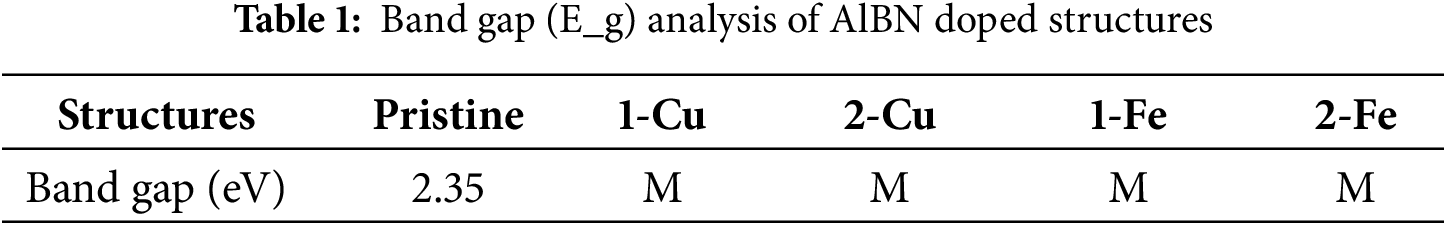
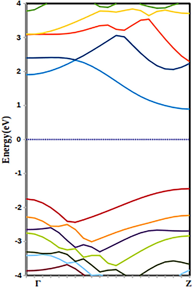
Figure 3: Band structure of AlBN-pristine
1Cu–AlBNR DOS (Fig. 4) states that Cu creates shallow impurity states near the Fermi level, reducing the band gap. 2Cu–AlBNR gives increased Cu concentration that leads to overlapping states at the Fermi level, indicating metallic behavior. 1Fe–AlBNR demonstrates that Fe doping introduces strong Fe-3d and N-2p hybrid states near the Fermi level, enhancing conductivity. 2Fe–AlBNR gives a high density of Fe-3d states at the Fermi level, confirming a complete metallic transition and strong hybridization shown in Fig. 5. Pristine AlBNR shows a clear band gap around the Fermi level, confirming semiconducting behavior shown in Fig. 6.
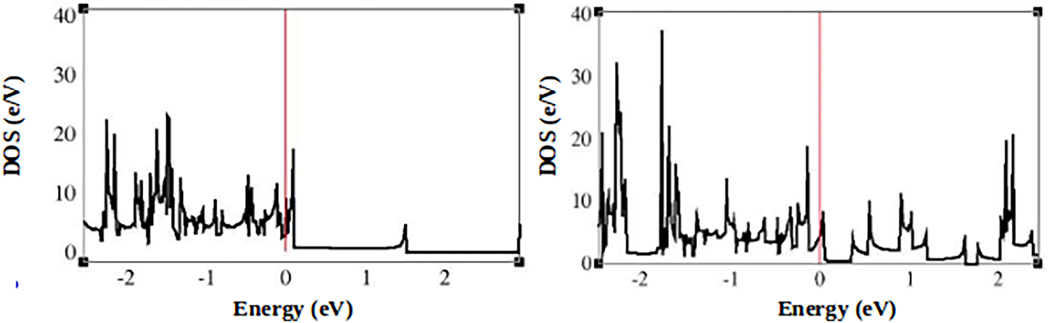
Figure 4: Density of states of AlBN with doped Cu atoms [1 atom (left) & 2 atoms (right)]
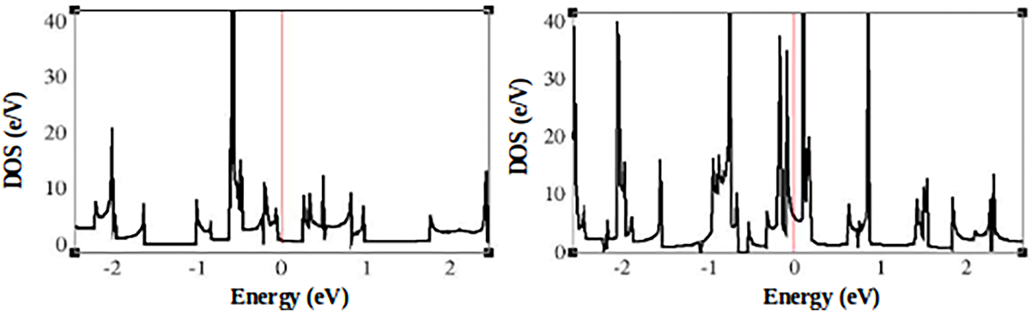
Figure 5: Density of states of AlBN with doped Fe atoms [1 atom (left) & 2 atoms (right)]
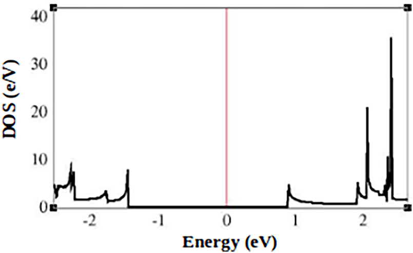
Figure 6: Density of states of AlBN-pristine
The Projected Density of States (PDOS) shows the number of available electronic states per unit energy. The Fermi level, marked by the vertical dashed line, represents the energy level up to which electronic states are filled at 0 K. Fig. 7a shows the PDOS of 1–Cu doped AlBN. Several sharp peaks appear around the Fermi level. A finite DOS at εF indicates that Cu doping introduces metallic behavior. The Cu 3d states hybridize with AlBN orbitals, filling the band gap and improving conductivity. The strong peaks near εF suggest localized Cu-induced electronic states. Fig. 7b corresponds to 2–Cu doped AlBN. The PDOS intensity near εF increases compared to 1–Cu doping. A higher Cu concentration enhances metallicity and provides more conduction states. Interaction between Cu dopants broadens the states near εF, leading to slight electron delocalization. Fig. 7c shows the PDOS for 1–Fe–doped AlBN. The DOS near εF remains finite but with sharper, spin-split peaks. Fe 3d orbitals contribute strongly near εF, indicating magnetic and metallic behavior. Compared to Cu doping, Fe introduces more localized d-states, which may cause half-metallic or spin-polarized characteristics depending on spin configuration. Fig. 7d presents the PDOS of 2–Fe–doped AlBN. Broader peaks and a higher DOS at εF suggest enhanced metallicity due to Fe–Fe interactions. The overlap of Fe 3d states increases, promoting easier electron transport. Possible ferromagnetic coupling between Fe atoms may occur, depending on their arrangement. Fig. 7e shows pristine AlBN. A clear band gap is observed around εF, with no states present at the Fermi level. This confirms the semiconducting nature of undoped AlBN. The valence and conduction bands are well separated, as expected for a wide-bandgap 2D material.
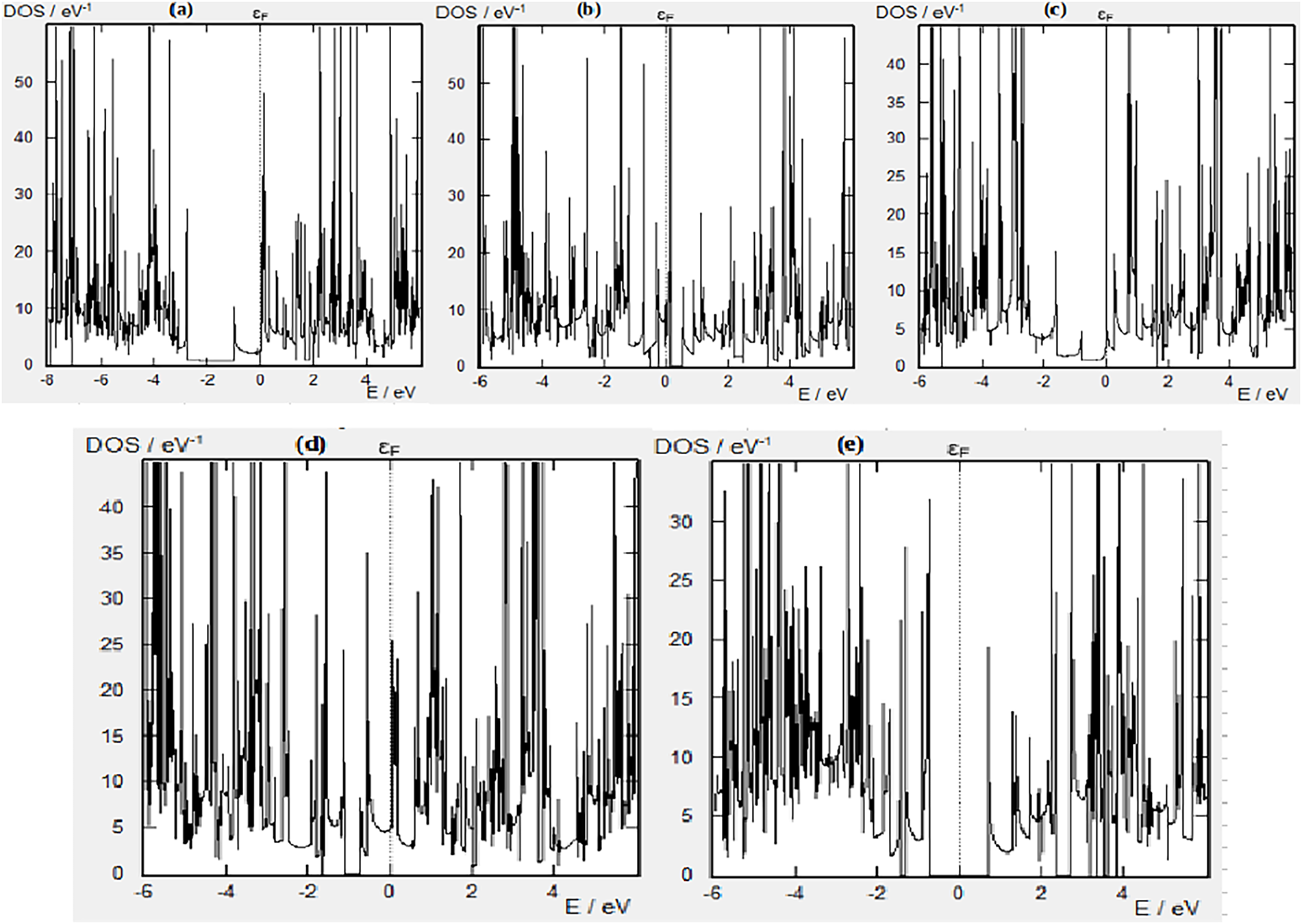
Figure 7: Projected density of states of AlBN with doped. (a) 1-Cu; (b) 2-Cu; (c) 1-Fe configurations; (d) 2-Fe and (e) Pristine configurations
The AlBN network in the proposed structure was observed to maintain a highly ordered hexagonal lattice, which ensures strong covalent bonding and low defect density. The vertical stacking of layers, combined with high-k dielectric materials such as Aluminium Boron N (AlBN), helps optimize the interlayer spacing. This optimization reduces electron hopping losses and minimizes impedance mismatches. This tight integration contributed to enhanced mechanical stability and uniform charge transport across the interconnects. Figs. 8–10 illustrate the optimized geometries of AlBN structures. Fig. 8 shows Cu-doped configurations (a) 1-Cu and (b) 2-Cu. Fig. 9 presents Fe-doped configurations (a) 1-Fe and (b) 2-Fe, and Fig. 8 depicts the pristine AlBN structure. It is designed using Quantum ATK. It is atomistic models of materials, molecules, or nanostructures that are constructed, optimized, and analysed using computational simulations. These structures allow us to study the properties and behaviors of materials at the atomic scale. Below is an overview of simulated nanostructures.
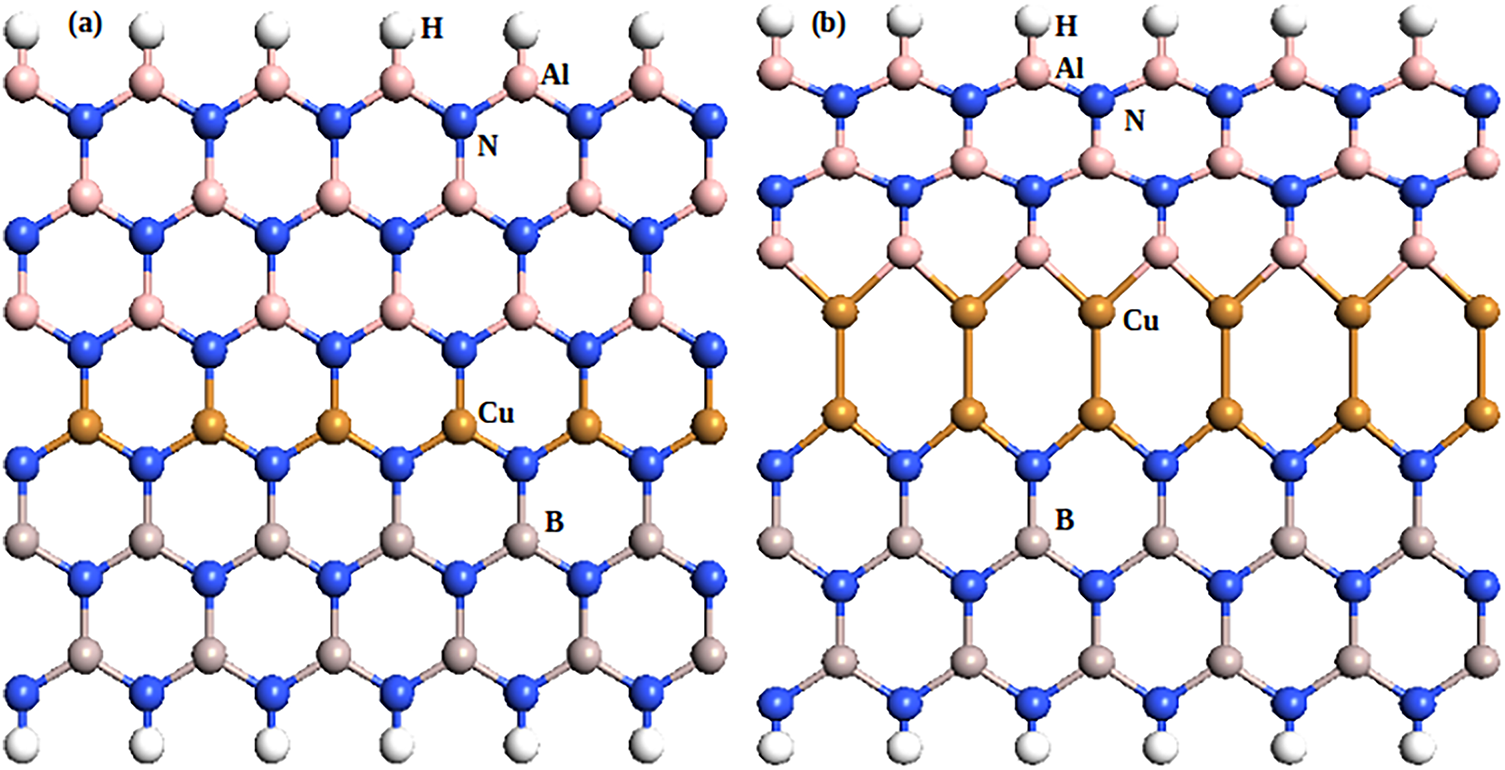
Figure 8: AlBN-Cu structure [(a) 1-Cu doped (left) & (b) 2-Cu doped (right)]
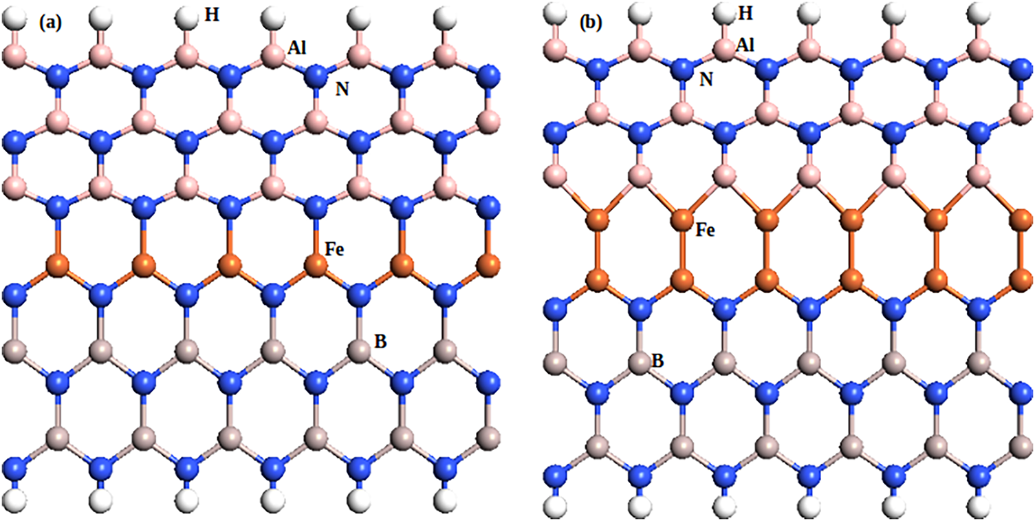
Figure 9: AlBN-Fe structure [(a) 1-Fe doped (left) & (b) 2-Fe doped (right)]
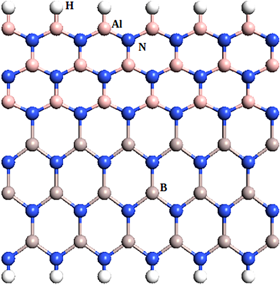
Figure 10: AlBN pristine structure
As compared to conventional Cu interconnects, which suffer from electromigration and mechanical degradation at smaller dimensions, these AlBN structures demonstrated superior mechanical strength due to its high Young’s modulus and intrinsic tensile strength. The addition of high-k dielectrics provided additional rigidity, reducing the likelihood of structural deformations under high-frequency operations and thermal fluctuations.
The absence of borders between grains, which are typical in Cu, further improved the structural reliability of structures. Doping copper into a nanostructure is primarily used to modify its electronic properties. It often leads to changes in the optical, electrical, and magnetic behaviors of the material. Copper doping can fine-tune a material’s characteristics by introducing localized electron states within the structure. This allows for enhanced conductivity, altered emission wavelengths, or improved catalytic activity, depending on the material being doped.
The binding energy values indicate the thermodynamic stability of the AlBN structures. Higher (more negative) binding energy suggests stronger atomic bonding and greater structural feasibility during synthesis. These computed values correlate with experimental deposition methods such as sputtering or atomic layer deposition (ALD), where stable configurations with favorable binding energies are more likely to form and sustain under realistic growth conditions.
Doping Fe often leads to changes in a material’s conductivity, optical absorption, and catalytic activity. It introduces additional electron states within the band gap, which modify the electronic behavior. Fe incorporation can also influence the lattice structure and overall stability, depending on the host material and doping concentration. The structural flexibility and atomic thinness of AlBNs allowed for smooth incorporation with current VLSI fabrication processes, particularly for sub-7 nm node technologies. The calculated total energies (Etotal) for pristine and metal-doped AlBN structures are listed in Fig. 11. The pristine AlBN exhibits a total energy of −2339.27 eV, which becomes more negative upon Cu or Fe doping, indicating improved structural stabilization due to the incorporation of metal atoms. For Cu-doped systems, the total energy decreases from −3534.27 eV (1Cu) to −4602.70 eV (2Cu), suggesting that the system becomes increasingly stable with higher Cu concentration. Similarly, for Fe doping, Etotal values of −2947.33 eV (1Fe) and −3425.73 eV (2Fe) also indicate enhanced binding upon addition of Fe atoms. These results are consistent with the higher cohesive (binding) energy of Fe relative to Cu, confirming that Fe doping strengthens the atomic network and improves the structural integrity of AlBN nanoribbons, which is advantageous for high-speed and thermally stable nanoscale interconnect applications.
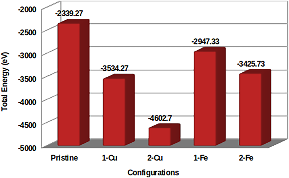
Figure 11: Total energies (ETotal) analysis of AlBN doped structures
The values of the binding energy, taken from the simulation data from Fig. 12, indicate that AlBNs with high-k dielectrics exhibit stronger interlayer bonding compared to other nanostructures. The high-k materials provide additional stability through strengthening the van der Waals connections between layers, reducing layer separation and improving mechanical integrity. Higher binding energy values indicate stronger structural cohesion, ensuring greater resistance to delamination under high-frequency operation.
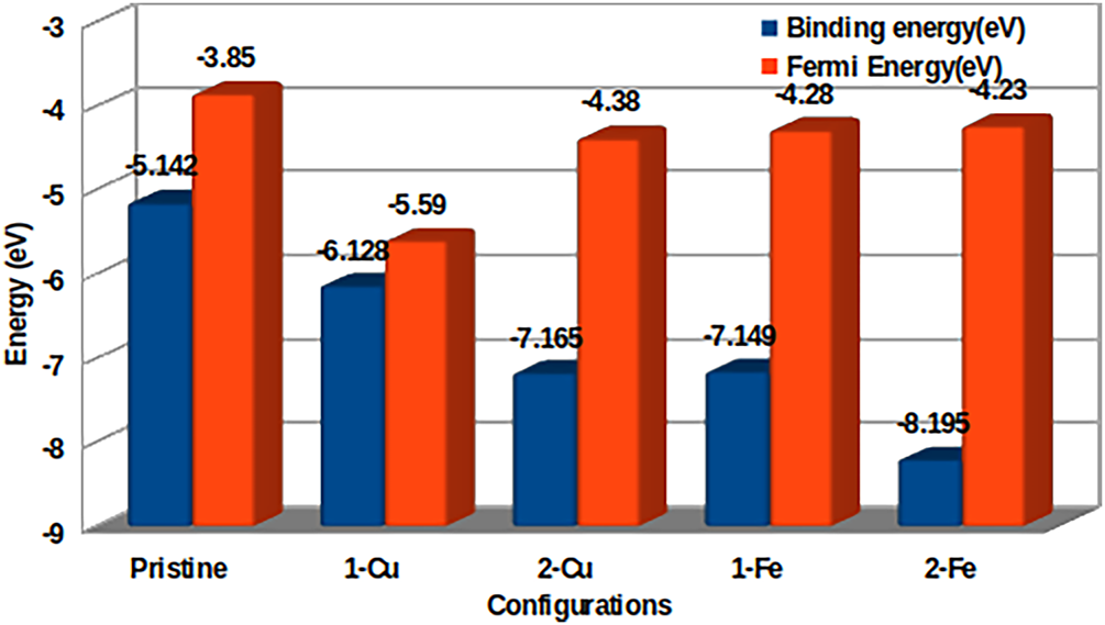
Figure 12: Binding (E_be) & fermi (E_Fe) energies analysis of AlBN doped structures
The stability of a nanostructure is primarily determined by its binding energy, with more negative binding energy values indicating stronger atomic interactions and higher stability. In the given figure, the pristine structure (−5.12 eV) exhibits a highly negative binding energy, signifying a naturally stable configuration. When a single copper atom is introduced (1-Cu, −6.12 eV), the binding energy becomes slightly more negative, suggesting a minor increase in stability due to structural stability caused by Cu doping. However, when two Cu atoms are introduced (2-Cu, −7.16 eV), the E_be increases significantly (less negative), indicating a substantial stability. This sharp increase suggests that excessive Cu doping strengthens the overall molecular integrity, possibly due to increased lattice strain and charge redistribution effects. Iron (Fe) doped, on the contrary, has a clear pattern of stability. The configuration with a single Fe atom (1-Fe, −7.1.49 eV) has a more stable value, and it has a greater negative binding energy than the pure form of the material, which suggests that Fe doping enhances the stability of the material’s structure and enhances the bonds between atoms. The E_be becomes more negative with the addition of two Fe atoms (2-Fe, −8.1 eV), meaning stability is increased slightly. However, 2-Fe is still more stable than 2-Cu, meaning Fe has a more positive intermolecular structure interaction and better relieves strain than Cu. The differences in stability between Cu- and Fe-doped structures are due to the differences in electronic and atomic interactivity each dopant contributes. The presence of Fe atoms improves the stability, primarily due to the more robust atomic contacts and suitability of the Fe atoms in the lattice structure. However, excessive Fe doping (2-Fe) imposes less stress on the structure and consequently increases stability. To summarize, 2-Fe remains the most stable positive-density structure modification path. In contrast, double Cu doping (1-Cu) results in significant instability, which clearly indicates that over-quantity Cu substitution is detrimental to structural stability. Further, Cu doping can be optimized in the study so as not to diminish performance, whereas Fe appears to be a reasonable dopant to stabilize material structure. Maintaining structural stability is crucial for material functionality and performance in real-world applications, and the results obtained in this study may serve as a valuable tool for developing next-generation interconnect materials.
The resistance of an interconnect is determined by the conductivity, length, and cross-sectional area of the material. Unlike Cu, AlBN nanoribbons demonstrate ballistic transport properties where the scattering of electrons is reduced and resistance is lower. The proposed AlBN structure minimizes this effect by utilizing vertical stacking, reducing interlayer resistance and improving conductivity. The impact of doping is also considered, where Fe doping demonstrates the lowest resistance due to its near-metallic bandgap, while excessive Cu doping leads to increased resistance and instability. Here, we have considered only rq and Nch values.
Inductance has a vital part in high-speed interconnect performance, affecting signal integrity and delay. Due to their nanoscale structure and vertical stacking, AlBN interconnect modelling exhibits a combination of kinetic inductance (lq) and magnetic inductance (LM). Here we have considered only kinetic inductance.
Capacitance affects crosstalk noise, power dissipation and signal propagation delay. The capacitance of AlBN interconnects is composed of electrostatic capacitance (CE) and quantum capacitance (Cq). In VLSI circuits, this will lead to less power dissipation, better signal integrity, and reduced RC latency.
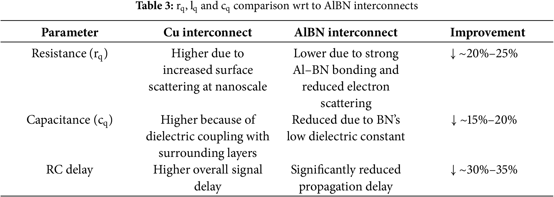
Equivalent series combination of Electrostatic capacitance (CE)—due to geometry and dielectric environment. Quantum capacitance (CQ)—arises from finite density of states. Below, the values of rq, cq, lq and delay obtained and shown in Table 2. The values are presented in the table which is used for the analysis of the interconnect circuits. The interconnect modeling is represented in Fig. 13. Table 3 states rq, lq and cq comparison wrt to AlBN Interconnects. Since it impacts quickly when signals are transmitted, as well as overall circuit performance, propagation delay is an important attribute in high-speed VLSI interconnects.
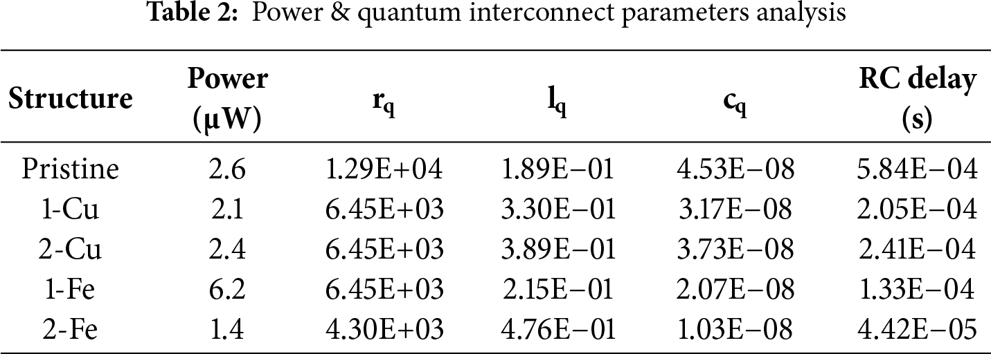
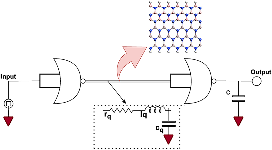
Figure 13: Equivalent RLC interconnect model
The resistance (rq), capacitance (cq), and inductance (lq) of the connector material have the greatest effects. Elmore delay for length L of the connection is given by,
The efficiency of traditional copper interconnects used in high-speed applications is limited primarily by the increasing RC delay and electromigration effects, which lead to a significant increase in propagation delay when looking at the nanoscale. As a viable alternative, AlBN structures are being developed to potentially reduce resistance, increase electron mobility, and reduce signal distortion in the new interconnect model. The electrical and mechanical properties of the material, which are often changed due to doping constituents such as Cu and Fe, greatly influence the effectiveness of the interconnects based on AlBNs. The AlBN structure is compatible with existing CMOS back-end-of-line (BEOL) processes due to its low-temperature fabrication, chemical stability, and ability to integrate with conventional Al metallization. This ensures seamless incorporation into current semiconductor manufacturing workflows without major process modifications. The AlBN interconnects exhibit reduced capacitive coupling and lower line-to-line interference, leading to improved noise margins and minimized cross-talk compared to Cu. This enhancement is primarily due to the high dielectric strength and uniform interface quality of the BN layer, which effectively suppresses unwanted signal coupling in dense interconnect layouts. AlBN interconnects maintain relatively stable thermal conductivity and exhibit a slower increase in resistance with temperature compared to Cu. This stability ensures reliable performance under high thermal stress conditions in advanced VLSI systems. Future experimental studies could employ advanced characterization techniques capable of resolving atomic structure, bonding, and local electronic states in AlBN systems. High-resolution transmission electron microscopy (HRTEM) and scanning transmission electron microscopy (STEM), combined with energy-dispersive X-ray spectroscopy (EDX) or electron energy loss spectroscopy (EELS), could directly visualize dopant incorporation. Nano-Raman spectroscopy would further enable the detection of strain distributions, phonon confinement effects, and chemical bonding variations associated with different dopant concentrations.
This research presents a novel AlBN structure with High-K Dielectric Material as a promising alternative to conventional copper interconnects for nanoscale VLSI circuits. By leveraging the superior electronic and structural properties of AlBN, our proposed interconnect modelling significantly reduces resistance (4.30E+03) Ω, inductance (4.76E−01), and capacitance (1.03E−08), leading to enhanced signal integrity and minimized power dissipation (1.4 μW). The results obtained indicate that Fe doping (2-Fe) offers the best stability and electronic performance, with minimal resistance, making it the most suitable doping strategy for interconnects. Overall, the proposed AlBN architecture successfully addresses the limitations of Cu interconnects, providing a scalable and energy-efficient solution for next-generation semiconductor technology. With continuous research and development, proposed interconnects have the potential to revolutionize semiconductor technology, enabling faster, more efficient, and scalable VLSI circuits in future computing and communication applications.
Acknowledgement: The authors would like to thank the VIT for providing laboratory support and computational facilities required for this research.
Funding Statement: The authors received no specific funding for this study.
Author Contributions: Rame Gowda D. N., Trisha J. K. designed the study and developed the methodology. Varshini M., Poornesha S. Shetty, Arpan Shah performed simulations, data analysis, and experiments. Mandar Jatkar, Mallikarjun P. Y. contributed to writing, reviewing, and editing the manuscript. All authors reviewed the results and approved the final version of the manuscript.
Availability of Data and Materials: The datasets generated and/or analyzed during the current study are available from the corresponding author on reasonable request.
Ethics Approval: This article does not involve studies with human participants or animals; therefore, ethics approval is not required.
Conflicts of Interest: The authors declare no conflicts of interest to report regarding the present study.
References
1. Xu P, Huang H, Zou F, Xie L. Applying the high-k dielectric materials in vertical multilayer graphene nanoribbon (V-MLGNR) based interconnect for improving transmission performance. Micro Nanostruct. 2024;193:207926. doi:10.1016/j.micrna.2024.207926. [Google Scholar] [CrossRef]
2. Zhao WS, Cheng ZH, Wang J, Fu K, Wang DW, Zhao P, et al. Vertical graphene nanoribbon interconnects at the end of the roadmap. IEEE Trans Electron Devices. 2018;65(6):2632–7. doi:10.1109/ted.2018.2822664. [Google Scholar] [CrossRef]
3. Gambino JP. Copper interconnect technology for the 22 nm node. In: Proceedings of 2011 International Symposium on VLSI Technology, Systems and Applications; 2011 Apr 25–27; Hsinchu, Taiwan. p. 1–2. doi:10.1109/vtsa.2011.5872228. [Google Scholar] [CrossRef]
4. Hughes KJ, Iyer KA, Bird RE, Ivanov J, Banerjee S, Georges G, et al. Review of carbon nanotube research and development: materials and emerging applications. ACS Appl Nano Mater. 2024;7(16):18695–713. doi:10.1021/acsanm.4c02721. [Google Scholar] [CrossRef]
5. Nishad AK, Sharma R. Performance improvement in SC-MLGNRs interconnects using interlayer dielectric insertion. IEEE Trans Emerg Topics Comput. 2015;3(4):470–82. doi:10.1109/tetc.2015.2486748. [Google Scholar] [CrossRef]
6. Zou F, Pan Z, Xu P. Modeling and performance analysis of coupled multilayer graphene nanoribbon (MLGNR) interconnects with intercalation doping. Microelectron J. 2023;141:105971. doi:10.1016/j.mejo.2023.105971. [Google Scholar] [CrossRef]
7. Das S, Bhattacharya S, Das D, Rahaman H. A short review on graphene nanoribbon interconnect. In: Proceedings of the 2020 International Symposium on Devices, Circuits and Systems (ISDCS); 2020 Mar 4–6; Howrah, India. p. 1–7. doi:10.1109/isdcs49393.2020.9263018. [Google Scholar] [CrossRef]
8. Hummel RE. Electromigration and related failure mechanisms in integrated circuit interconnects. Int Mater Rev. 1994;39(3):97–112. doi:10.1179/imr.1994.39.3.97. [Google Scholar] [CrossRef]
9. Cheng P, Mao LF, Shen WH, Yan YL. Electromigration failures in integrated circuits: a review of physics-based models and analytical methods. Electronics. 2025;14(15):3151. doi:10.3390/electronics14153151. [Google Scholar] [CrossRef]
10. Yin Y, Liu B, Zhang Y, Han Y, Liu Q, Feng J. Wafer-scale nanoprinting of 3D interconnects beyond Cu. ACS Nano. 2025;19(18):17578–88. doi:10.1021/acsnano.5c00720. [Google Scholar] [PubMed] [CrossRef]
11. Nishad AK, Sharma R. Analytical time-domain models for performance optimization of multilayer GNR interconnects. IEEE J Sel Top Quantum Electron. 2014;20(1):17–24. doi:10.1109/jstqe.2013.2272458. [Google Scholar] [CrossRef]
12. Jatkar M, Jha KK, Patra SK. Fermi velocity and effective mass variations in ZGaN ribbons: influence of Li-passivation. IEEE Access. 2021;9:154857–63. doi:10.1109/access.2021.3128294. [Google Scholar] [CrossRef]
13. Agrawal Y, Chandel R, Kumar MG. Performance analysis of multilayer graphene nano-ribbon in current-mode signaling interconnect system. In: Proceedings of the 2015 IEEE International Symposium on Nanoelectronic and Information Systems; 2015 Dec 21–23; Indore, India. p. 297–302. doi:10.1109/inis.2015.44. [Google Scholar] [CrossRef]
14. Politou M, Wu X, Contino A, Soree B. Multi-layer graphene interconnect. In: Proceedings of the 2016 IEEE International Interconnect Technology Conference/Advanced Metallization Conference (IITC/AMCIEEE); 2016 May 23–26; San Jose, CA, USA. p. 200–2. doi:10.1109/IITC-AMC.2016.7507731. [Google Scholar] [CrossRef]
15. Sharda V, Agarwal RP. Analysis of graphene nanoribbon (GNR) interconnects with multi-gate device technology for VLSI applications. In: Proceedings of the 2015 IEEE UP Section Conference on Electrical Computer and Electronics (UPCON); 2015 Dec 4–6; Allahabad, India. p. 1–6. doi:10.1109/upcon.2015.7456742. [Google Scholar] [CrossRef]
16. Xu C, Li H, Banerjee K. Modeling, analysis, and design of graphene nano-ribbon interconnects. IEEE Trans Electron Devices. 2009;56(8):1567–78. doi:10.1109/ted.2009.2024254. [Google Scholar] [CrossRef]
17. Sanaeepur M. Crosstalk delay and stability analysis of MLGNR interconnects on rough surface dielectrics. IEEE Trans Nanotechnol. 2019;18:1181–7. doi:10.1109/TNANO.2019.2945354. [Google Scholar] [CrossRef]
18. Jatkar M, Jha KK, Patra SK. DFT investigation on targeted gas molecules based on zigzag GaN nanoribbons for nano sensors. IEEE J Electron Devices Soc. 2022;10:139–45. doi:10.1109/jeds.2022.3144014. [Google Scholar] [CrossRef]
19. Nemu A, Singh S, Jha KK, Tyagi N, Jaiswal NK. First-principles design of high speed nanoscale interconnects based on GaN nanoribbons. Comput Mater Sci. 2025;249:113625. doi:10.1016/j.commatsci.2024.113625. [Google Scholar] [CrossRef]
20. Krishna MS, Singh S, Gupta S, Kumar Kaushik B. Nanointerconnect design using unsaturated edged antimonene nanoribbons: DFT-NEGF analysis. IEEE Trans Electron Devices. 2024;71(8):5066–72. doi:10.1109/ted.2024.3408780. [Google Scholar] [CrossRef]
21. Yadav B, Srivastava P, Sharma V. Substitutionally doped zigzag germanium sulfide nanoribbon for interconnect applications: DFT-NEGF approach. IEEE Trans Nanotechnol. 2024;23:809–14. doi:10.1109/tnano.2024.3504601. [Google Scholar] [CrossRef]
22. Agrawal S, Srivastava A, Kaushal G. Performance metrics of doped graphene nanoribbons based nanoscale interconnects: DFT and NEGF analysis. Solid State Commun. 2024;380(3):115389. doi:10.1016/j.ssc.2023.115389. [Google Scholar] [CrossRef]
23. Rub Ansari H, Nizamuddin M, Manzoor S, Mishra P. Performance analysis of doped zigzag graphene nanoribbon-based device for practical electronic applications using first principle approach. Comput Mater Sci. 2025;247(24):113464. doi:10.1016/j.commatsci.2024.113464. [Google Scholar] [CrossRef]
24. Jatkar M, Mallikarjun PY. Optimized Cu/Fe doped Boron Nitride Nanoribbons as nanoscale interconnect: DFT investigation. Mater Sci Semicond Process. 2025;186(1):109050. doi:10.1016/j.mssp.2024.109050. [Google Scholar] [CrossRef]
Cite This Article
 Copyright © 2026 The Author(s). Published by Tech Science Press.
This work is licensed under a Creative Commons Attribution 4.0 International License , which permits unrestricted use, distribution, and reproduction in any medium, provided the original work is properly cited.
 Downloads
 Citation Tools