 Submit a Paper
 Propose a Special lssue
 Open Access
ARTICLE

N×N Clos Digital Cross-Connect Switch Using Quantum Dot Cellular Automata (QCA)
1 Amity University, Lucknow, 226028, India
2 The Oxford College of Engineering, Bangalore, 560019, India
* Corresponding Author: Amita Asthana. Email:
Computer Systems Science and Engineering 2023, 45(3), 2901-2917. https://doi.org/10.32604/csse.2023.030548
Received 29 March 2022; Accepted 18 May 2022; Issue published 21 December 2022
 View Full Text
 Download PDF
Abstract
Quantum dot cellular automata (QCA) technology is emerging as a future technology which designs the digital circuits at quantum levels. The technology has gained popularity in terms of designing digital circuits, which occupy very less area and less power dissipation in comparison to the present complementary metal oxide semiconductor (CMOS) technology. For designing the routers at quantum levels with non-blocking capabilities various multi-stage networks have been proposed. This manuscript presents the design of the N×N Clos switch matrix as a multistage interconnecting network using quantum-dot cellular automata technology. The design of the Clos switch matrix presented in the article uses three input majority gates (MG). To design the 4 × 4 Clos switch matrix, a basic 2 × 2 switch architecture has been proposed as a basic module. The 2 × 2 switching matrix (SM) design presented in the manuscript utilizes three input majority gates. Also, the 2 × 2 SM has been proposed using five input majority gates. Two different approaches (1&2) have been presented for designing 2 × 2 SM using five input majority gates. The 2 × 2 SM design based on three input majority gate utilizes four zone clocking scheme to allow signal transmission. Although, the clocking scheme used in 2 × 2 SM using three input MG and in 2 × 2 SM approach 1 using five input MG is conventional. The 2 × 2 SM approach 2 design, utilizes the clocking scheme in which clocks can be applied by electric field generators easily and in turn the switch element becomes physically realizable. The simulation results conclude that the 2 × 2 SM is suitable for designing a 4 × 4 Clos network. A higher order of input-output switching matrix, supporting more number of users can utilize the proposed designs.Keywords
This manuscript presents an original design and simulation of cross connect switch using quantum-dot cellular automata (QCA). QCA based contention and their implementation requires an expeditious simulation and design layout tool to determine the functionality of QCA circuits. In QCA technology, the transmission of signal eventuates due to electrostatic interaction force among the adjacent and diagonally located electrons in the QCA cell. The flow of charge in a QCA wire, and also the crossovers available in the simulated designs have been discussed. The simulation results of the proposed basic logic gates-based network switches have been presented in the manuscript.
The objective of this work is to design:
• 2:1 multiplexer circuit using 19 cells only
• 1:2 demultiplexer using 21 nano cells
• 2 × 2 switch using multiplexers as basic switching block or matrix (SM) by using a reduced number of cells
• 4 × 4 Clos switching network using proposed 2 × 2 SM
• 2 × 2 SM using five input majority gates using two different approaches. The proposed work is significant and opens new possibilities for designing various non-blocking quantum switches.
The manuscript is arranged as follows: a brief investigation of QCA related work is in Section 2. Section 3, provides the operating principle of QCA. Section 4, illustrates the proposed circuits’ design. In Section 5, the simulation results of the proposed 2 × 2 switching matrix using three input MG, the non-blocking Clos switch matrix design and a 2 × 2 switch matrix using five input majority gates with both the approaches have been explained. The outcomes and findings are in Section 6. In Section 7, the simulation results are compared with published work. Finally, the conclusion and future work is presented in Sections 8 and 9 respectively.
Quantum-dot cellular automata is an important tool to design digital circuits at the quantum level. It is an emerging nanotechnology to design the circuits and networks with feature size at nanometers level with less power consumption [1]. The concept of QCA was first introduced in 1993 [2]. An even parity generator and even parity checker have been designed using quantum-dot cellular automata by reducing the cell count, area and latency [3]. Similarly, various digital circuits like binary coded decimal adders [4–6], multiplexers, multipliers i.e., have been designed and investigated with reduced cell count and area. Different digital circuits such as full adder and multiplexer have also been proposed using a majority gate with simple and rotated cell, which are fault-tolerant against single-cell omission and extra cell deposition effects [7]. Serial and parallel memory designs have been proposed for QCA implementation [8,9]. QCA implementation is a powerful tool for designing the nanoscale circuits, and hence it can also be used to design the field-programmable gate arrays configurable logical blocks [10]. A four-bit microprocessor has been proposed using quantum-dot cellular automata [11]. Green computing has also been performed using reversible logic in quantum-dot cellular automata. The design of the router to transmit the data packets has been done using multilayer nanocircuits by adopting reversible logic abstraction [12]. The correct data transmission depends primarily on the parity data added to the endowed bitstream. To effectuate this the 3-bit odd and even parity generators and checkers have been designed elicited from QCA, x-or /x-nor gates using a congruent layer of cells [13]. An error detecting even parity generator and checker were designed using QCA with reduction in cell count, area, latency along with better bit error coverage [14]. The execution of clocked QCA circuits has been scrutinized based on the Bayesian probabilistic model in terms of steady-state polarization and thermal specifications of the cells, in which the nodes being random variables and the links between the nodes represent the dependent functions [15]. It has been well validated that the performance of data communication through networks depends on the switch matrix architecture. The performance of various switches can also be examined using nano digital circuits. Wire crossing networks have been proposed using dynamic programming to contribute to different interconnections at different times [16]. Some reversible logic-based circuits have been proposed for the authentication of the users using Feynman gates which operates on the principle of 2 × 2 mapping. The designed nanocircuit can be utilized for the certainty of user palm vein image [17]. Several routing and distributive networks have been proposed using sequential circuits like 2-bit counters or 3-bit counters. Also, the wire crossing concept has been elaborated by the researchers to dispatch the data on the correct route by providing special clock phases [18]. Various multistage networks along with delta network have been realized using QCA designer embedding 2 × 2 switching element (SE) as the basic unit based on multiplexers [19]. To modify the interconnectivity hamming code generator QCA circuits have also been implemented [20]. Many concepts of blocking and non-blocking switch configurations have been proposed and delineated using quantum-dot cellular automata for nano-communication. Furthermore, the Banyan switch network has been proposed as a multi-stage network using two input and two output crossbar switches. The number of inputs and outputs of a crossbar switch can be increased using multi-stage design but using the 2 × 2, as a basic switching element. The basic SE can be designed efficiently to improve the cell count, area and number of majority gates [21]. A butterfly switch matrix architecture was proposed, based on a basic switching element using a modified majority gate being fully utilized and hence successfully administered the cost efficiency and adaptability of the proposed structure. The butterfly switch matrix networks implemented using quantum-dot cellular automata has been compared with the CMOS technology for the same 2 × 2, 4 × 4 and 8 × 8 switch matrix networks in terms of area and power. The total energy dissipation and cost function analysis vanquished the existing CMOS designs [22]. To achieve the high data rate on-chip scheduler has been proposed using a round Robin algorithm [23]. The basic logic primary structure in quantum-dot cellular automata is a majority voter, which is not defined as a universal logic. A tile-based design has been proposed as a basic logic component. Cells must be grouped into tiles of the same clock, which shifts the abstraction level in the QCA layout process from cell-based design to tile-based design [24]. It was suggested that clocking in QCA is different from clocking in conventional CMOS circuitry. Every circuit needs to be clocked in the quantum dot to allow for the transmission of signals. These clocks are applied by electric field generators beneath the substrate [25]. The connection chain concept has been introduced to avoid blocking of Clos switch matrix by dispatching rearrangement algorithms.
The algorithms presented in the paper put an upper bound on the number of rearrangements and also manifests the condition of only one rearrangement for the switch to perform as an optimum non-blocking switch [26]. The speculative demonstration has been presented by configuring 4 × 4 microring (MRRs), switch and select (S&S) to evaluate the performance of a 16 × 16 Clos network using 12.5 Gbps PAM4 signal across the network and 1.1 dB maximum power retribution at a bit error rate of 1.03 × 10⁻⁷ [27]. Clos network has been analyzed to reduce the power consumption by switching off some switches temporarily depending on the traffic parameters at any time, also few routing techniques have been developed to improve the blocking probability, propagation time and delay along with shuffle exchange networks have been suggested for multiple stages interconnecting switch matrix [28–30]. For providing flexibility in terms of giving clocks to the nanocircuits the overall design has been segregated in various grids in clockwise and anticlockwise directions. The suggested algorithm enhances the accuracy in placement of the nano cells and accomplishes flawless routing [31,32]. In addition to the famous three-input majority voter circuit, five input majority contributors and seven input majority contributors were also designed [33–36]. To reduce the computation power and to increase the fault tolerance of nanocircuits, different atomic scale technologies have been presented considering few physical realities for preferable utilization of majority gates [37].
The quantum dot cellular automata technology is basically designing the digital circuits using quantum cells. This technology can be seen as the future of nano computation. The circuit works on the majority voter and inverter gates. Each QCA cell consists of four quantum dots with two mobile electrons which can tunnel between the dots. The electrons due to their coulombic repulsion force occupy the corner positions. The QCA cell and their possible polarizations to maintain the minimum energy, are shown in Fig. 1.
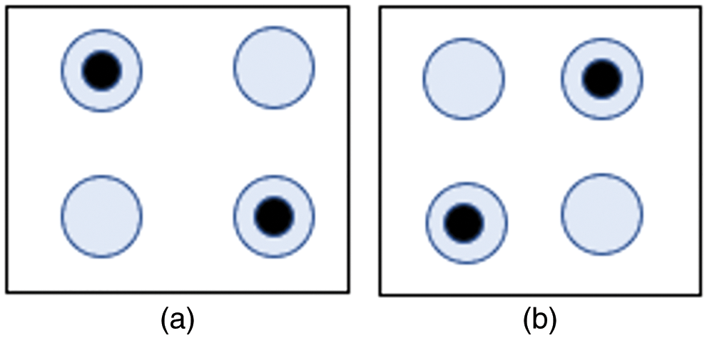
Figure 1: (a) and (b) are Binary zero & binary one respectively
QCA has the potential to replace conventional dominating technologies such as CMOS and guarantees exceptionally low-power, exceedingly dense and prompt structures at the nanoscale. This work includes a robust QCA based on multiple input majority gate. QCA is an emerging concept in computational nanotechnology for the realization of quantum computer using arrays of four-dot cells. The objective is to design the systemized and energy efficient circuits in terms of cell-count, complexity and latency as compared to the previously published depictions. The circuits can be modified over their conventional design due to technology change in QCA. This design in contrast to its counterparts uses a robust crossover scheme. The simulations of the proposed designs were done using simulation engines of the QCA-Designer. The proposed designs are compared to the previous QCA works.
The multiplexer can be used as a line selector in the switching matrix. The proposed multiplexer has been designed to have a smaller number of cells and less area at the nanometer scale as shown in Fig. 2. The circuit is composed of three majority gates along with an inverter. Whenever select input is zero the data from i0 is being selected. Similarly, the output follows the input i2 for the select input one. The reduction of two cells just below the input cell i0 and just above the input cell i1, does not make any changes to the output. In this paper, a new five input majority gate 2:1 multiplexer has been proposed. The energy between two cells depends on various positions of electrons between the adjacent cells. The previously designed multiplexer [35] is using 73 nano-cells and, in the current work, only 16 cells are being utilized. The paper proposes 73 cell 2:1 multiplexer nanocircuit with 76734 nano-meters square area. The 16 cells proposed 2:1 multiplexer circuit simulation has been performed by coherence vector simulation engine, which took only six seconds with five iterations to converge the initial steady state polarization at 1 K temperature. The calculated circuit area of proposed circuit is 11514 nano-meters square.
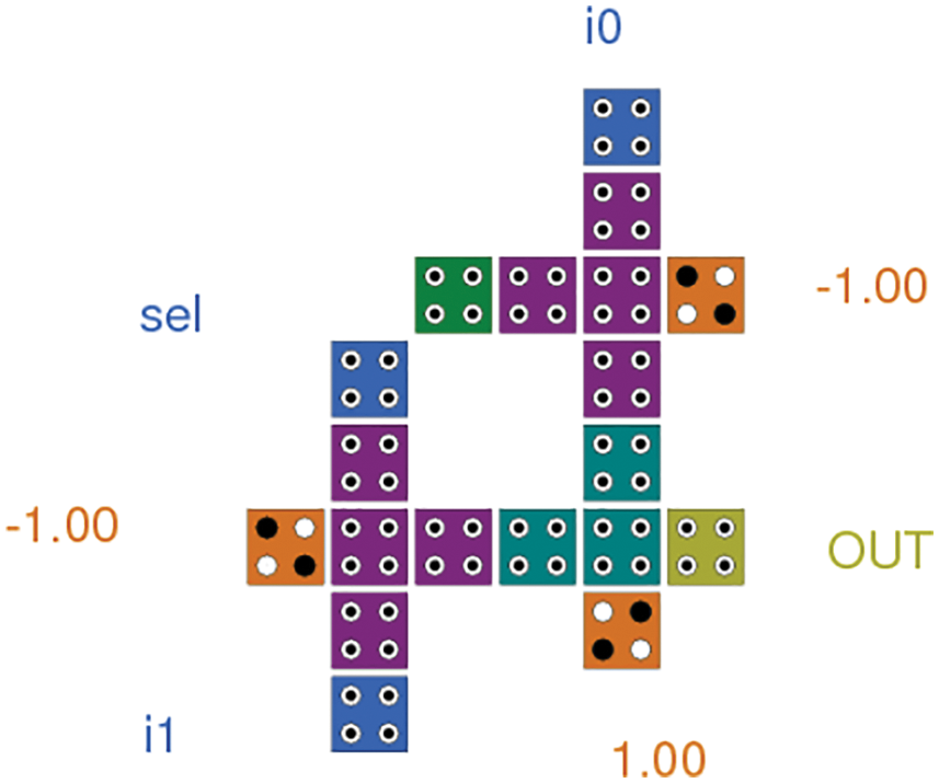
Figure 2: Three input majority gate 2:1 multiplexer
The proposed multiplexer uses only one majority gate or majority voter (MV) and both negative and positive fixed polarities have been given as shown in Fig. 3.
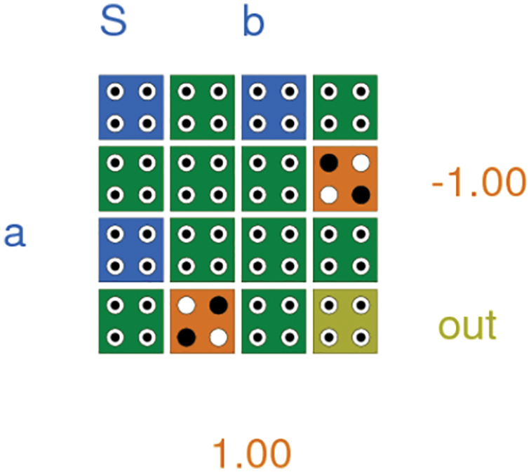
Figure 3: Five input majority gate 2:1 multiplexer
The inputs i0 and i1 are designated as a and b respectively and the select line as S.
The demultiplexer design as shown in Fig. 4 uses two majority gates and two inverters. Depending on the select input, the inputs are transferred to the output.
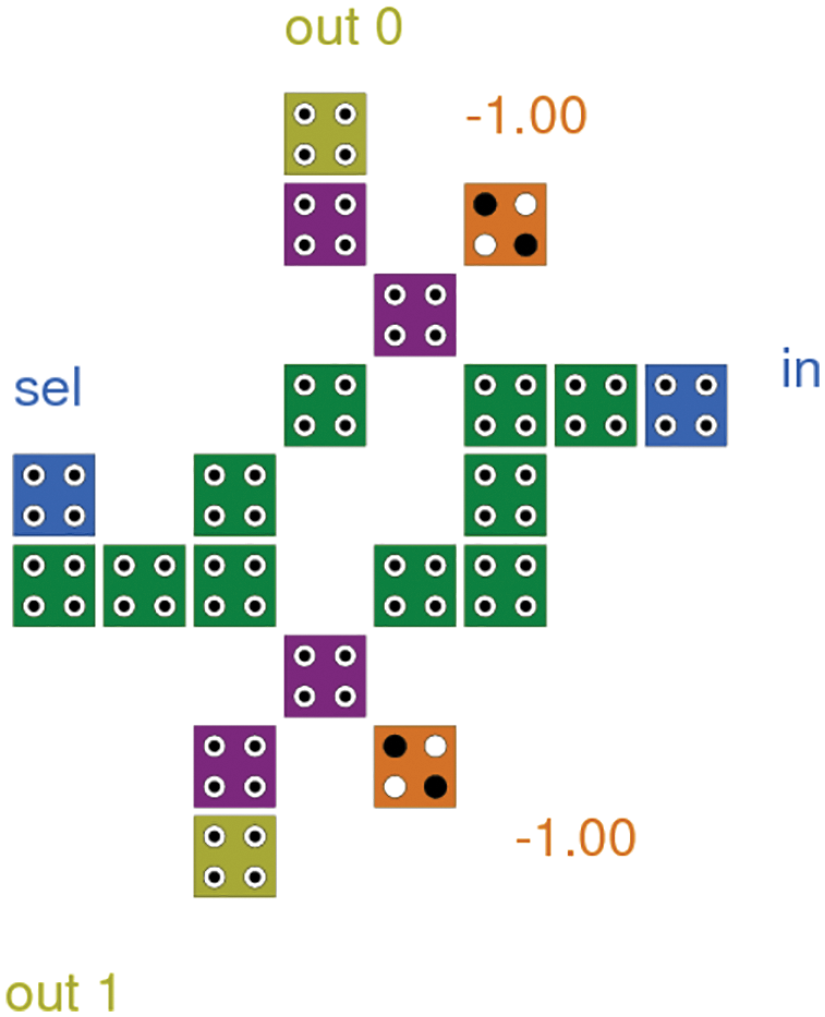
Figure 4: 2:1 Demultiplexer
4.3 The 2 × 2 Switching Matrix
The 2 × 2 switching matrix circuit using three input majority gates is shown in Fig. 5. The proposed 2 × 2 switch has been designed using six, 3-input majority gates. Two inputs are represented as x1 and x2, whereas the outputs are out1 and out2. The circuit has been designed using two inverters to invert the select lines as input to corresponding majority gates. The majority gates with negative polarities are AND gates and the majority gates with positive polarities are OR gates and hence constitutes the two multiplexer circuits and hence the 2 × 2 switching matrix.
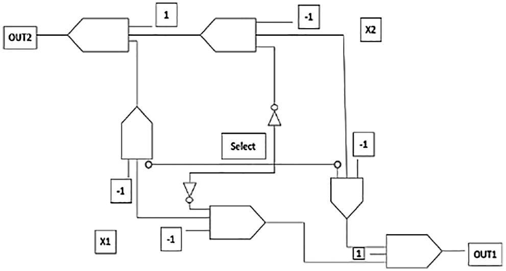
Figure 5: The circuit layout of proposed 2 × 2 switching matrix
The circuit uses six majority gates along with two inverters.
The outputs are selected based on the select input as simulated in Fig. 6. The majority gate based QCA depiction can be represented by the following equation set.
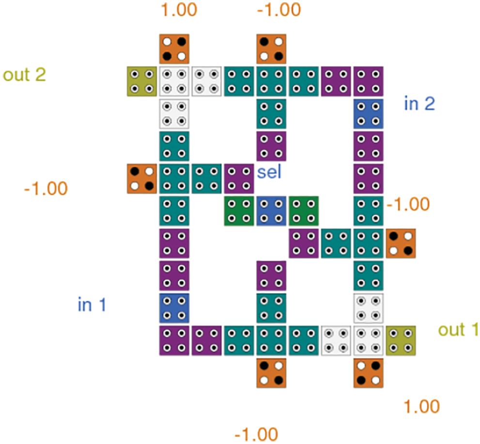
Figure 6: The simulated circuit layout 2 × 2 switching matrix
The basic advantage of multistage networks is that using small modules the large switches can be designed. The proposed 2 × 2 SM can be used to design the multistage Clos network. The Clos switch matrix has been designed using the proposed 2 × 2 SM as a basic element. The circuit has been constructed using four 2 × 2 switch matrices, and hence supports four cross four switch matrix. The design can be extended to 8 × 8 and even more to support several inputs and outputs. The designed circuit layout of the 4 × 4 Clos switch matrix using the proposed 2 × 2 switching matrix is shown in Fig. 7. There are two stages of four 2 × 2 switches in which O1 and O2 are the first stage upper 2 × 2 switch outputs and O3 and O4 are the lower 2 × 2 switch outputs. The outputs of first stage are connected to the inputs of the second stage. The second stage outputs are z1, z2, z3 and z4. A total of two inputs and two outputs for each block has been designed and connectivity of the four 2 × 2 switch modules have been shown in the simulation.
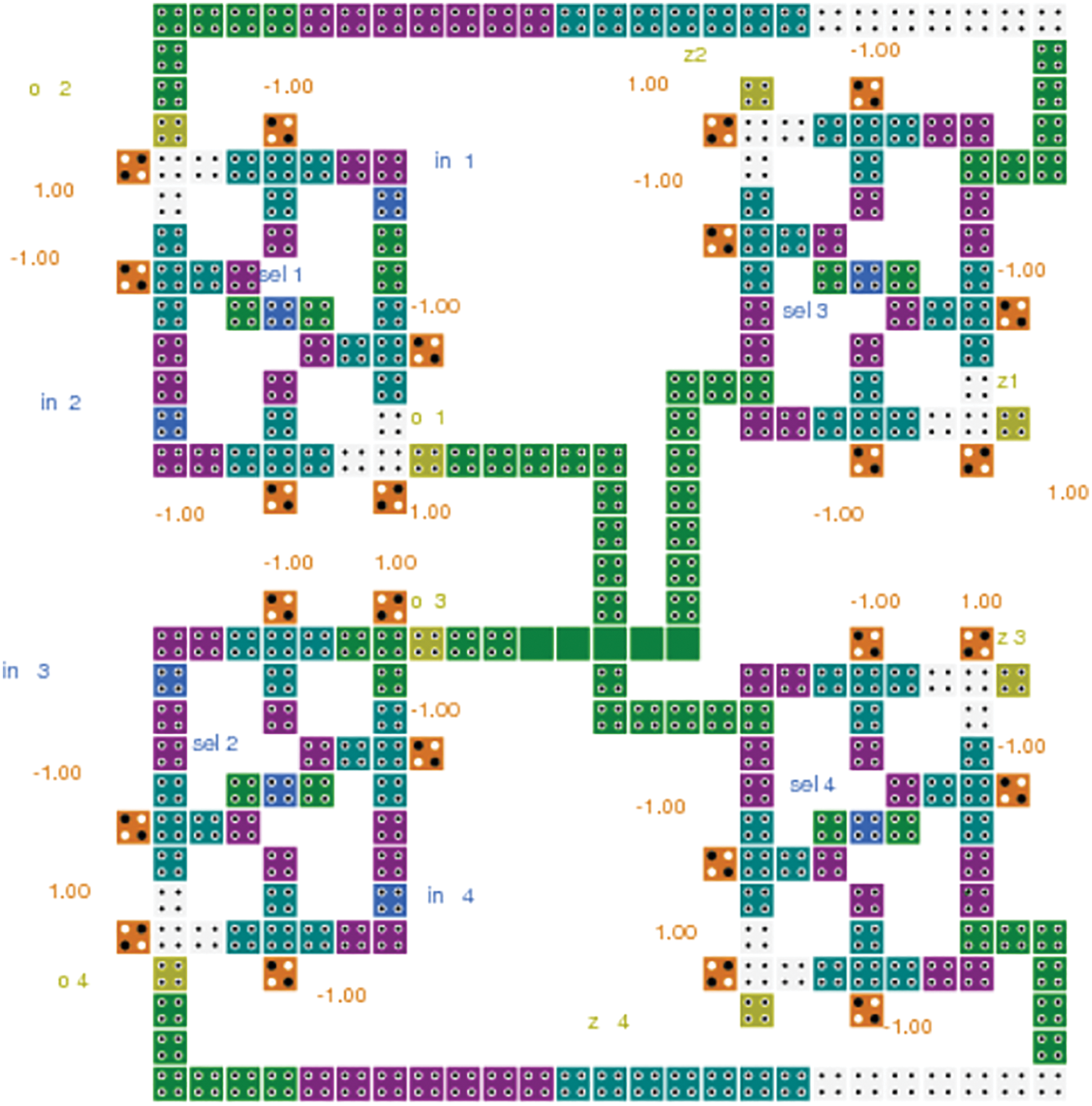
Figure 7: The simulated circuit layout of 4 x 4 Clos switch matrix using proposed 2 × 2 SM
4.5 2 × 2 SM Using Five Input Majority Gate
Next, we can also design the 2 × 2 switch matrix using five inputs majority gate. The proposed switch uses only two five input majority gates to work as 2 × 2 switch matrix as depicted in Fig. 8.
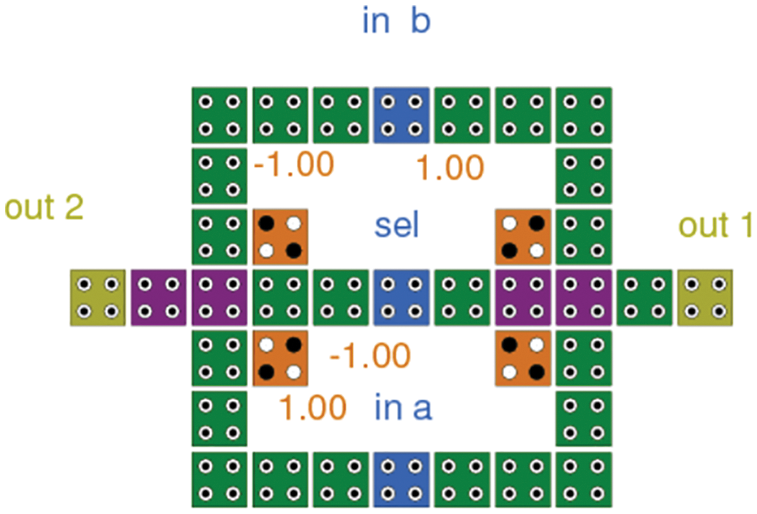
Figure 8: The circuit layout in QCA Designer for 2 × 2 switching matrix using five input majority gate (approach 1)
Three inputs being given as A, B and Sel with the two outputs as out1 and out2. The logical expression for the SM can be defined as follows s,
The next approach for making a 2 × 2 SM is shown in Fig. 9.
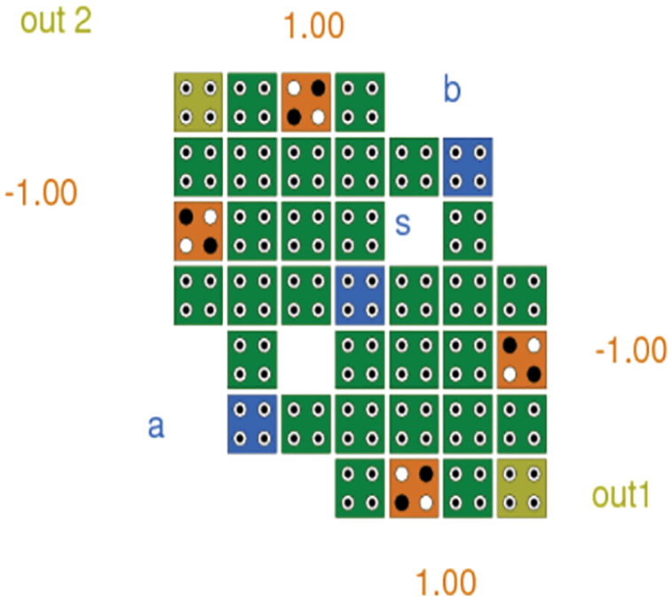
Figure 9: The circuit layout in QCA Designer for 2 × 2 switching matrix using five input majority gate (approach 2)
The circuit functions following the input on the select line. In the two input and two outputs, proposed SM, the two inputs are a and b. The two outputs are out1 and out2, which are controlled by s input as shown in the simulation result.
Our proposed design has been implemented using QCA Designer, using coherence vector simulation engine, other parameters used as default parameters. Three clock zones have been used so that the output is delayed by 0.75 cycles. When Sel is zero, i0 will be selected making output equal to i0. Fig. 10 shows the simulation result of the 3-input majority gate 2:1 multiplexer.
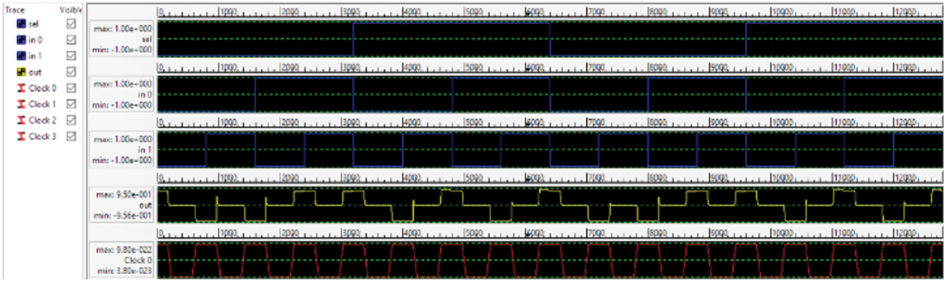
Figure 10: Simulation result of the 3-input majority gate 2:1 multiplexer
Fig. 11 shows five input majority gate using QCA cells on the QCA Designer tool the simulation supports the tile-based design in which the clocking beneath the cells gets much easier from the physical implementation point of view. Although, in the circuit, only one clock zone has been used for simulation.
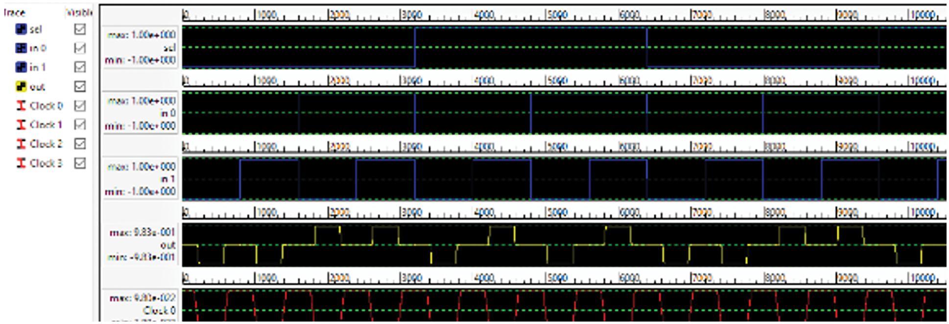
Figure 11: Simulation result of 5 input majority gate based 2:1
Fig. 12 shows the simulation result for the 2:1 demultiplexer where all the four clock zones have been used utilizing the default parameters at 1 K temperature with a coherence vector simulation engine. The simulation results are following the standard input-output results.
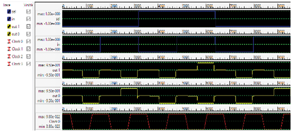
Figure 12: Simulation result of 1:2 Demultiplexer
Fig. 13 represents the simulation of 2 × 2 switch matrix in which four clock zones have been used. Hence there is a delay of one clock cycle.
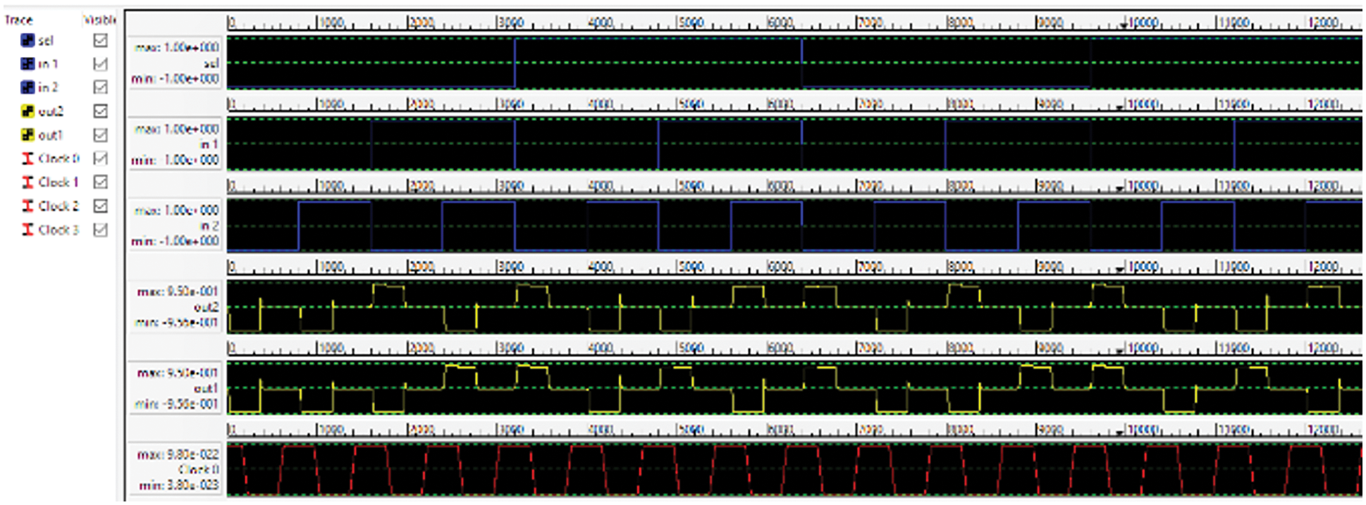
Figure 13: QCA simulation of proposed 2 × 2 SM
The proposed design layout of Clos switch matrix is simulated using QCA Designer tool by coherence vector simulation method at 1 K temperature with default relaxation time of 1 × 10⁻¹⁵ seconds. The layer separation and relative permittivity is 11.5 nanometers and 12.9, respectively. The simulated layout consists of three layers: main cell layer, middle cell layer and the upper layer. The main cell layer has been constructed using 277 normal cells and 2 vertical cells. The middle layer has been designed using 2 cells only, in which both the cells are vertically aligned. The upper layer has been simulated using five cells in which there are two vertical cells and three crossover cells. The complete circuit layout is having one cross over which is an advantage in itself. There are 24 majority gates and eight 2:1 multiplexer in the complete circuit layout.
The first stage outputs are O1, O2, O3 and O4 whereas the second stage outputs are z1, z2, z3 and z4 as shown in Fig. 14.
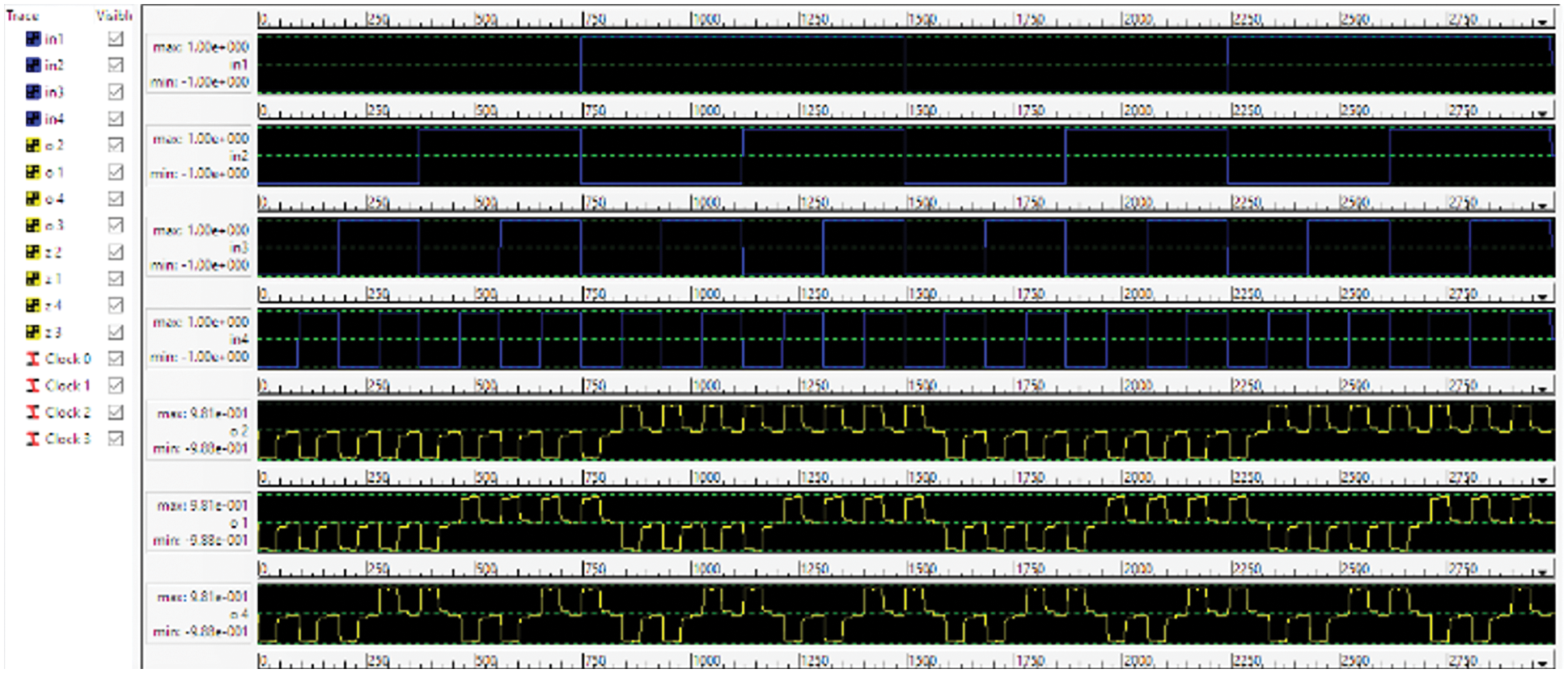
Figure 14: Evaluation diagram for Clos switch matrix
The simulation result shows the inputs A and B along with the sel input, two polarities inputs have been given as two more inputs for making it a combined 2 × 2 switch. The simulation results are in accordance as described. For out 1, if sel = 0, input ‘a’ will be selected and it appears on the output, whereas for sel = 1, input ‘b’ will appear on the output. Similarly, for out 2, if sel = 0, input ‘b’ will appear in output and for sel = 1, input ‘a’ will be visible as output.
For out 1, if sel = 0, input ‘a’ will be selected and it appears as the output, whereas for sel = 1, input ‘b’ will appear as the output. Similarly, for out 2, if sel = 0, input ‘b’ will appear as output and for sel = 1, input ‘a’ will be visible as output.
The simulation result shows the inputs A and B along with the sel input. Two polarities inputs have been given for making it a combined 2 × 2 switch as in Figs. 15 and 16.
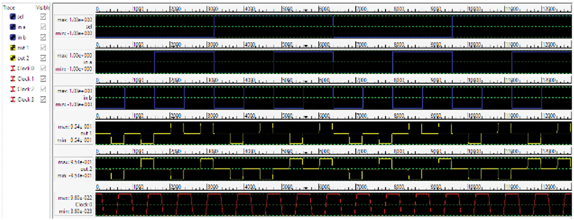
Figure 15: 2 × 2 SM output using 5 inputs majority gate (approach1)
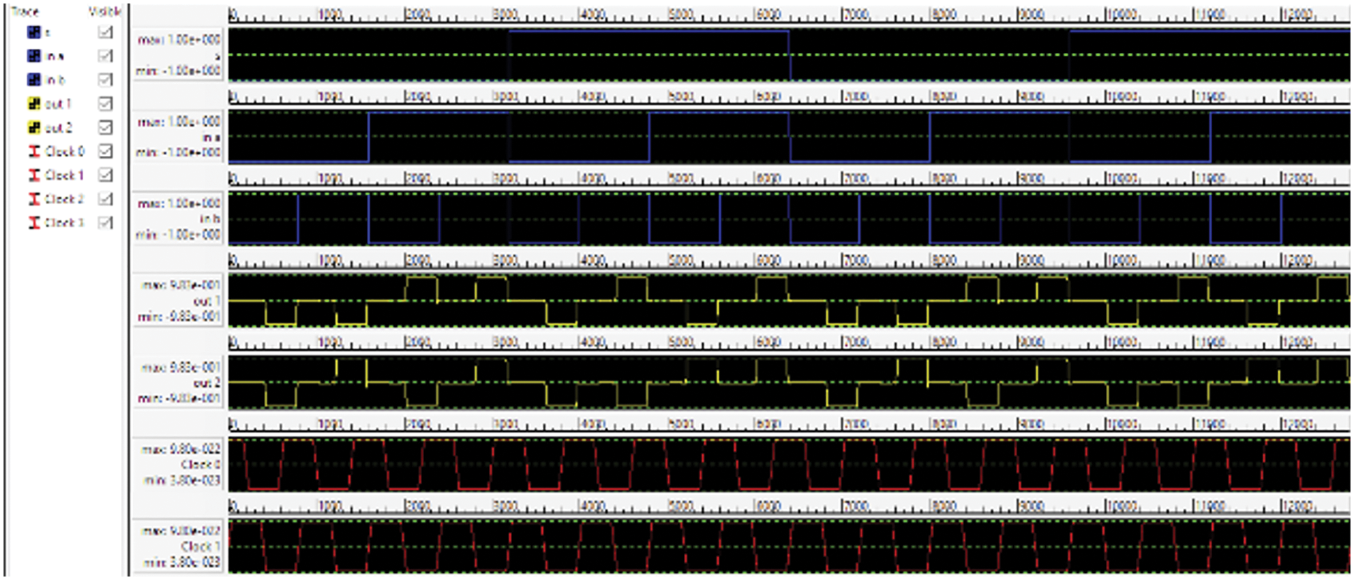
Figure 16: 2 × 2 SM output using 5 inputs majority gate (approach2)
The implementation of 8 × 8 clos switch has been presented using three stage interconnections has been demonstrated in Fig. 17. The middle stage includes four 2 × 2 switch matrices, whereas the first and third stages are utilizing two 4 × 4 switch matrices. Similarly, higher order of clos switch can be designed.
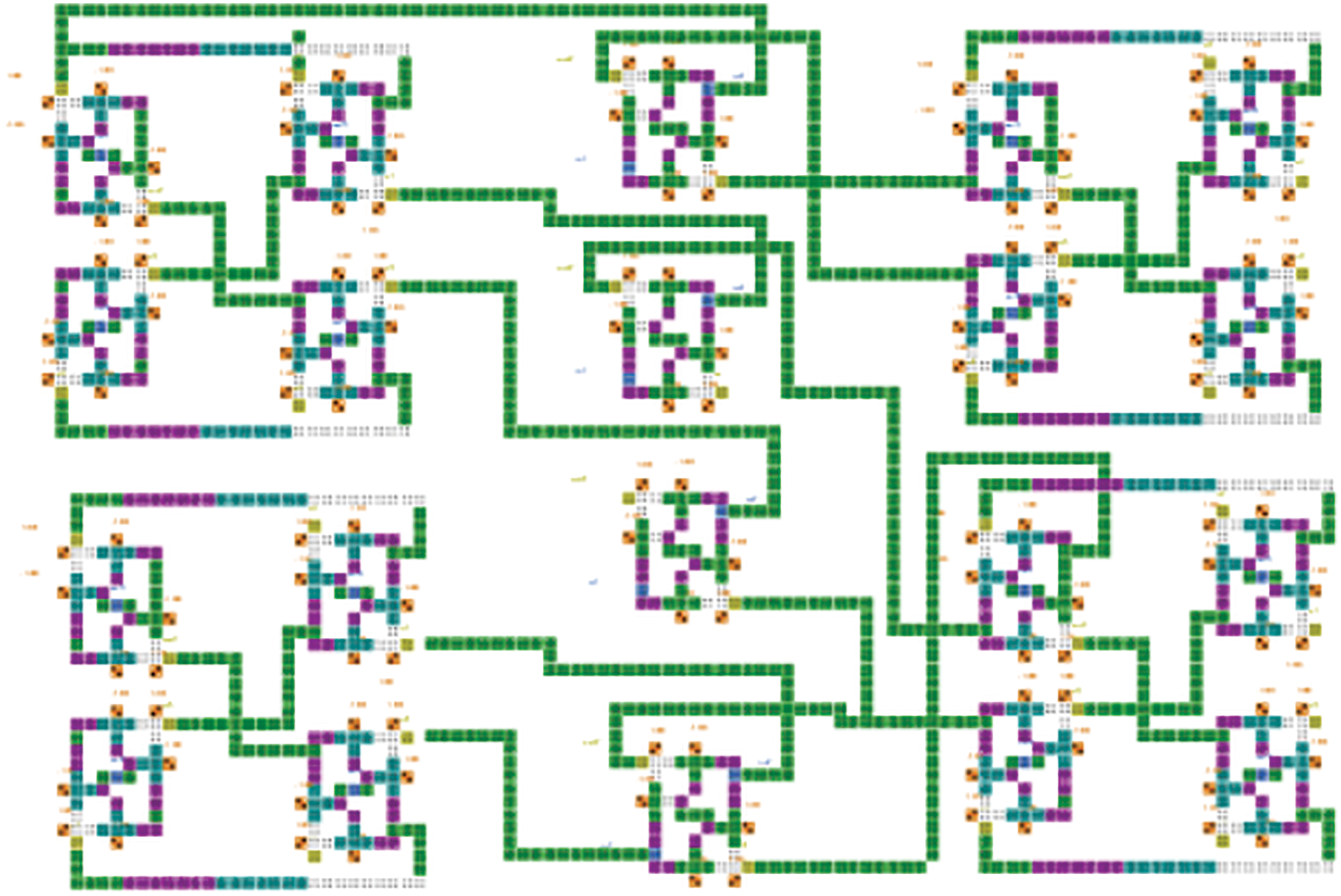
Figure 17: QCA simulation of 8 × 8 three stage Clos switch matrix
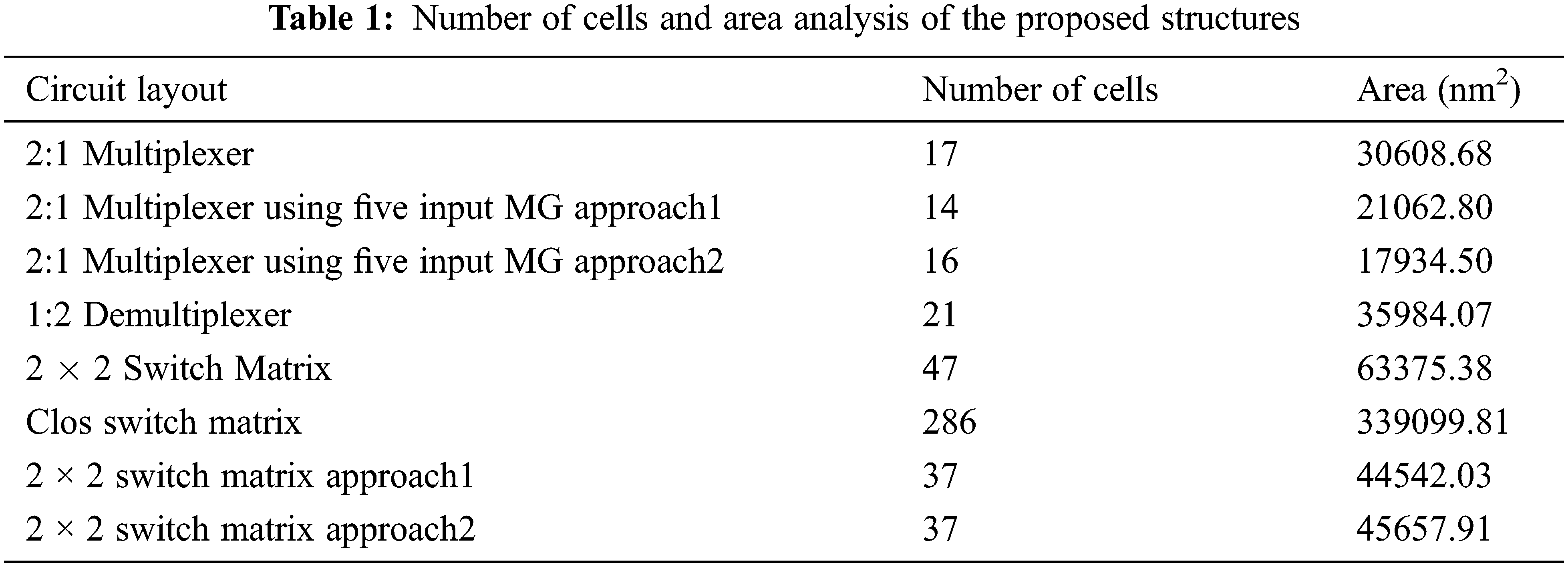
Tab. 1 summarizes all the circuits with number of cells and the area in nanometer square.
The manuscript shows the improvement in area, number of cells and cost of the QCA in comparison to the previous literatures available. Approach 1 and Approach 2 designs for 2 × 2 SMs are based on multi-input majority gates. Proposed SMs based on five input majority gates are less complicated in comparison to three input majority gate based SM. To improve the physical realization of nano circuits clocking arrangements have been taken care of, in case of approach 2 SM. It has been shown that it is not possible to clock single cells arbitrarily by these generators [24]. Therefore, cells are grouped in same clock arrangement as in design approach 2. This shifts the abstraction level in the QCA layout process from cell-based design to tile-based design [25] which is the de-facto standard to date.
• Approach 1 design- 2 × 2 SM, using approach 1 is not fully cell based but an improved version towards the clock partitioning technique.
• Approach 2 design- Approach 2 is similar to tile-based design.
The 2 × 2 SM approach 1 using five inputs majority gate (A, B, Sel, 1 and −1 polarizations) has been simulated using QCA Designer simulation software. Simulation has been performed for three inputs and two outputs with coherence vector simulation with 700000 samples, where 3000 samples have been recorded for graphing. The simulation took five iterations to converge the initial steady state polarization. 2 × 2 SM approach 2 has been simulated using three inputs and two outputs. The simulation took 6 iterations using coherence vector simulation. The same results can be obtained using bistable approximation method with simulation time of approximately 16 s, with layer separation of 11.5 nanometers. The 2 × 2 SM using three inputs majority gate has been simulated using coherence vector simulation method. Tab. 2 represents the improvement in cell count and area using all three design methodologies for all the SMs as proposed in the paper.
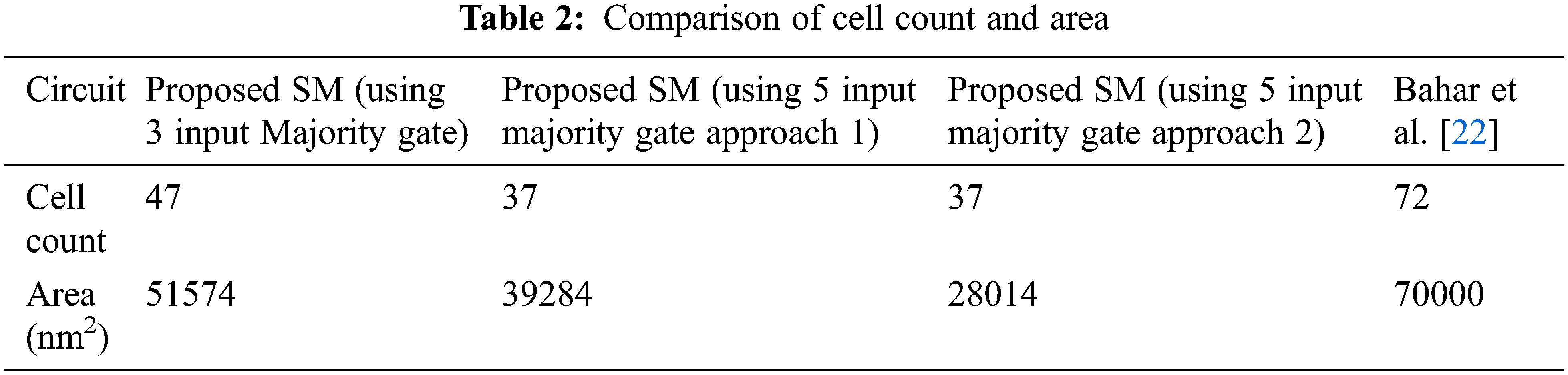
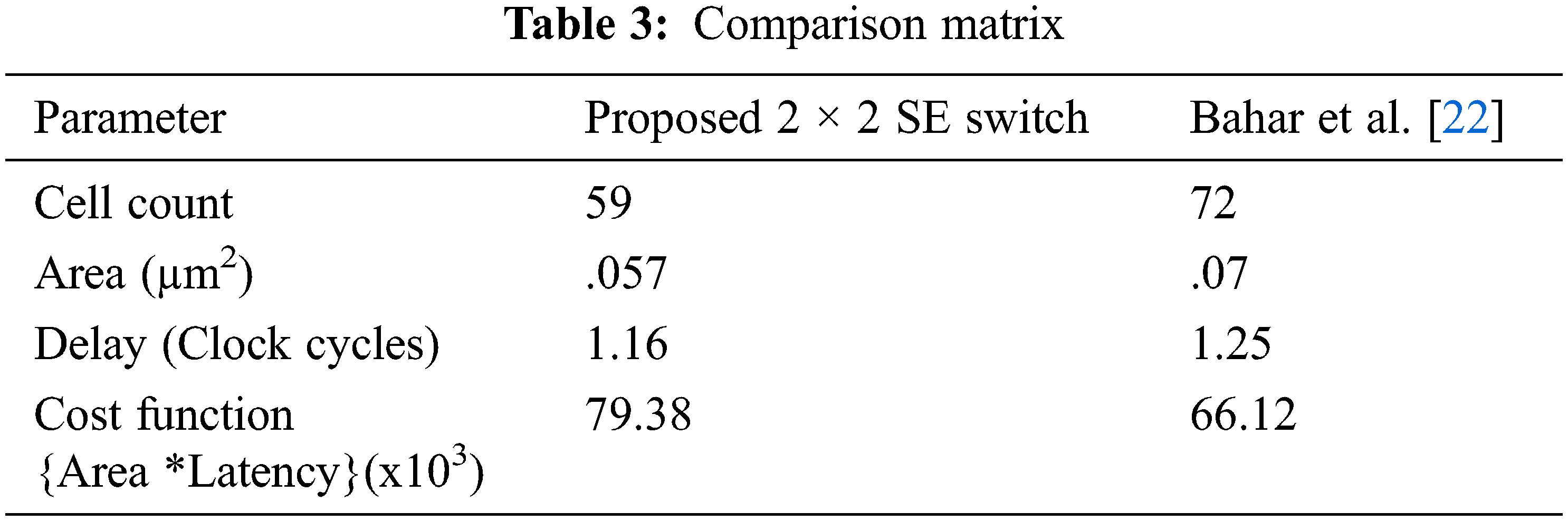
The proposed switch matrix has cell count advantage over [22], as well as the area can also be reduced to greater extent as represented in Tab. 3. All the proposed structures in this paper have been designed with reduced area and cell count in comparison to the previously published work. Also, the delay has been reduced with the compromise in number of majority gates.
In this article, we have proposed a Clos switch architecture for supporting several inputs and outputs. The architecture has been designed at the nanoscale level for multistage networks and simulated on quantum-dot cellular automata. Two approaches (1&2) used for designing five input majority gates. Due to the findings of the limitation of tile base design, we proposed a novel design (approach 1). The presented approach 2, is using the tile-based design for comparison. The simulation results have been verified for the proposed multistage interconnected network (MIN). Also, a new approach for five input majority gates for QCA has been proposed which in turn can reduce the clocking complications for designing on the real platform. Although the design process is based on the Coulombic force between the cells. The basic philosophy for the proposed design is to make the quantum switches for the development of nano-level networks. The proposed designs have been evaluated based on several cells and area. The result concluded that the 2 × 2 SE is suitable for designing a 4 × 4 Clos network. A higher number of input-output switching networks also can use the proposed design.
This article suggests the designing of nano-size switches based on digital circuits. The design of the 4 × 4 Clos network can be extended to 16 × 16 SM. The majority gate-based circuit can be used to design other non-blocking multistage switch networks. Also, the paper suggests a different architecture for designing the majority gate with increased number of inputs, similarly more possible cell orientations can be discovered for decreasing the area and power consumption. The design of the 4 × 4 Clos network can be extended to 16 × 16 and 32 × 32 SMs. The designed Clos switch matrix can be extended to zone partitioning technique using QCA-Designer tool.
Acknowledgement: The authors would like to thank Amity University, Lucknow campus for their technical support.
Funding Statement: The authors received no specific funding for this work.
Conflicts of Interest: The authors declare that no financial interests or personal assimilation has been considered which could influence the work in this paper.
References
1. J. C. Das and D. De, “Design of single layer banyan network using quantum-dot cellular automata for nanocommunication,” Optik Journal, vol. 172, pp. 892–907, 2018. [Google Scholar]
2. C. S. Lent, P. D. Tougaw, W. Porod and G. H. Bernstein, “Quantum cellular automata,” Nanotachnology, vol. 44, no. 1, pp. 49–57, 1993. [Google Scholar]
3. J. C. Das, D. De, S. P. Mondal, A. Ahmadian, F. Ghaemi et al., “QCA based error detection circuit for nano communication network,” IEEE Access, vol. 7, pp. 67355–67366, 2019. [Google Scholar]
4. G. Cocorullo, P. Corsonello, F. Frustaci and S. Perri, “Design of efficient BCD adders in quantum-dot cellular automata,” IEEE Transactions on Circuits and Systems, vol. 64, no. 5, pp. 575–579, 2017. [Google Scholar]
5. T. Zhang, V. Pudi and W. Liu, “New majority gate-based parallel BCD adder designs for quantum-dot cellular automata,” IEEE Transactions on Circuits and Systems, vol. 66, no. 7, pp. 1232–1236, 2019. [Google Scholar]
6. Z. Chu, Z. Li, Y. Xia, L. Wang and W. Liu, “BCD adder designs based on three-input XOR and majority gates,” IEEE Transactions on Circuits and Systems II, vol. 68, no. 6, pp. 1942–1946, 2021. [Google Scholar]
7. S. Ahmadpour, S. S. Mosleh and S. H. Rasouli, “The design and implementation of a robust single-layer QCA ALU using a novel fault-tolerant three-input majority gate,” The Journal of Supercomputing, vol. 76, no. 12, pp. 10155–10185, 2020. [Google Scholar]
8. V. Vankamamidi, M. Ottavi and F. Lombardi, “A line-based parallel memory for QCA implementation,” IEEE Transactions on Nanotechnology, vol. 4, no. 6, pp. 690–698, 2005. [Google Scholar]
9. V. Vankamamidi, M. Ottavi and F. Lombardi, “A serial memory by quantum-dot cellular automata (QCA),” IEEE Transactions on Computers, vol. 57, no. 5, pp. 606–618, 2008. [Google Scholar]
10. M. Raj, L. Gopalakrishnan, N. Naganathan and N. Ramasubramanian, “Configurable logic blocks and memory blocks for beyond-CMOS FPGA-based embedded systems,” IEEE Embedded Systems Letters, vol. 12, no. 4, pp. 113–116, 2020. [Google Scholar]
11. K. Walus, M. Mazur, G. Schulhof and G. A. Jullien, “Simple 4-bit processor based on quantum-dot cellular automata (QCA),” in IEEE Int. Conf. on Application-Specific Systems (ASAP’05), NW Washington, United States, pp. 288–293, 2005. [Google Scholar]
12. A. Kamaraj, Abinaya and S. Ramya, “Design of router using reversible logic in quantum cellular automata,” in Int. Conf. on Communication and Network Technologies, Sivakasi, India, pp. 249–253, 2014. [Google Scholar]
13. F. Ahmad, P. Ahmad and G. Bhat, “Design and analysis of odd- and even-parity generators and checkers using Quantum-dot Cellular Automata (QCA),” in Int. Conf. on Computing for Sustainable Global Development (INDIACom), New Delhi, India, pp. 187–194, 2015. [Google Scholar]
14. J. C. Das, D. De, S. P. Mondal, A. Ahmadian, F. Ghaemi et al., “QCA based error detection circuit for nano communication network,” IEEE Access, vol. 7, pp. 67355–67366, 2019. [Google Scholar]
15. S. Bhanja and S. Sarkar, “Probabilistic modeling of qca circuits using bayesian networks,” IEEE Transactions on Nanotechnology, vol. 5, no. 6, pp. 657–670, 2006. [Google Scholar]
16. C. R. Graunke, D. I. Wheeler, D. Tougaw and J. D. Will, “Implementation of a crossbar network using quantum-dot cellular automata,” IEEE Transactions on Nanotechnology, vol. 4, no. 4, pp. 435–440, 2005. [Google Scholar]
17. B. Debnath, J. C. Das, D. De, F. Ghaemi, A. Ahmadian et al., “Reversible palm vein authenticator design with quantum dot cellular automata for information security in nano communication network,” IEEE Access, vol. 8, pp. 174821–174832, 2020. [Google Scholar]
18. H. Hast, S. Khorbotly and D. Tougaw, “A signal distribution network for sequential quantum-dot cellular automata systems,” IEEE Transactions on Nanotechnology, vol. 14, no. 4, pp. 648–656, 2015. [Google Scholar]
19. M. A. Tehrani, F. Safaei, M. Moaiyeri and K. Navi, “Design and implementation of multistage interconnection networks using quantum-dot cellular automata,” Microelectronics Journal, vol. 42, no. 6, pp. 913–922, 2011. [Google Scholar]
20. J. Huang, G. Xie, R. Kuang, F. Deng and Y. Zhang, “QCA-based Hamming code circuit for nano communication network,” Microprocessors and Microsystems, vol. 84, no. 12, pp. 104237, 2021. [Google Scholar]
21. J. C. Das and D. De, “Design of single layer banyan network using quantum-dot cellular automata for nano-communication,” Optik, vol. 172, pp. 892–907, 2018. [Google Scholar]
22. A. N. Bahar and K. A. Wahid, “Design of an efficient N×N butterfly switching network in quantum dot cellular automata,” IEEE Transactions on Nanotechnology, vol. 19, pp. 147–155, 2020. [Google Scholar]
23. G. Thakur, M. Sarvagya and P. Sharan, “Design and implementation of crossbar scheduler for system-on-chip network in quantum dot cellular automata technology,” Internet Technology Letters, vol. 1, no. 6, pp. 1–6, 2018. [Google Scholar]
24. E. Blair and C. Lent, “Clock topologies for molecular Quantum-dot cellular automata,” Journal of Low Power Electronics and Applications, vol. 8, no. 3, pp. 31, 2018. [Google Scholar]
25. J. Haung and M. Ottavi, “Tile-based QCA design using majority-like logic primitives,” ACM Journal on Emerging Technologies in Computing Systems, vol. 1, no. 3, pp. 163–185, 2005. [Google Scholar]
26. H. N. Chiu, S. S. H. Ng, J. Retallick and K. Walus, “PoisSolver: A tool for modelling silicon dangling bond clocking networks,” in 2020 IEEE 20th Int. Conf. on Nanotechnology (IEEE-NANO), Montreal, Canada, pp. 134–139, 2020. [Google Scholar]
27. S. Ohta, “The number of rearrangements for Clos networks,” Theoretical Computer Science, vol. 814, pp. 106–119, 2020. [Google Scholar]
28. L. Y. Dai, Y. Hung, Q. Chengand and K. Bergman, “Experimental demonstration of PAM-4 transmission through microring silicon photonic clos switch fabric,” in Optical Fiber Communications Conf. and Exhibition (OFC), Sen Diego, pp. 1–3, 2020. [Google Scholar]
29. M. Glabowski, M. Sobieraj, M. Stasiak and M. D. Stasiak, “Modeling of Clos switching structures with dynamically variable number of active switches in the spine stage,” Electronics Journal, vol. 9, no. 7, pp. 1073, 2020. [Google Scholar]
30. A. Alatwi, N. Z. R. Ahmed, M. E. Ahmed and IS. Amiri, “Best candidate routing algorithms integrated with minimum processing time and low blocking probabilty for modern parallel computing systems,” Indonesian Journal of Electrical Engineering and Computer Science, vol. 19, no. 2, pp. 847–854, 2020. [Google Scholar]
31. O. A. Amodu, M. Othman, N. A. Yunus and Z. Hanapi, “A primer on design aspects and recent advances in shuffle exchange multistage interconnection networks,” Symmetry, vol. 13, no. 3, pp. 378, 2021. [Google Scholar]
32. B. Sen, J. Pal, J. Sharma, D. Bhowmik, A. K. Saha et al., “Regular clocking scheme based design of cost-efficient comparator in QCA,” Indonesian Journal of Electrical Engineering and Computer Science, vol. 21, no. 1, pp. 44–55, 2020. [Google Scholar]
33. D. Bhowmik, J. Pal, M. Goswami, P. Sen, A. K. Sahaand et al., “Systematic cell placement in quantum dot cellular automata embedding underlying regular clocking circuit,” IET Citcuits, Devices & Systems, vol. 15, no. 2, pp. 156–167, 2020. [Google Scholar]
34. V. J. Arulkarthick, A. Rathinaswamy and K. Srhari, “Design of BCD adder with five input majority gate for QCA,” Microprocessors and Microsystems, vol. 75, no. 11, pp. 103040, 2020. [Google Scholar]
35. S. Ahmadpour, M. Mosleh and S. R. Heikalabad, “An efficient fault-tolerant arithmetic logic unit using a novel fault-tolerant 5-input majority gate in quantum-dot cellular automata,” Computers & Electrical Engineering, vol. 82, no. 1, pp. 106548, 2020. [Google Scholar]
36. H. Mohammadi, K. Navi and M. Hosseinzadeh, “An efficient quantum-dot cellular automata full adder based on a new convertible 7-input majority-not gate,” IETE Journal of Research, vol. 2, no. 177, pp. 1–9, 2020. [Google Scholar]
37. M. Behrooz, D. Abedi and J. Ghassem, “Majority-logic, its applications, and atomic-scale embodiments,” Computers and Electrical Engineering, vol. 83, pp. 106562, 2020. [Google Scholar]
Cite This Article
 Copyright © 2023 The Author(s). Published by Tech Science Press.
This work is licensed under a Creative Commons Attribution 4.0 International License , which permits unrestricted use, distribution, and reproduction in any medium, provided the original work is properly cited.
 Downloads
 Citation Tools