
 Submit a Paper
 Propose a Special lssue
 Open Access
ARTICLE

A Low Common-Mode Voltage Virtual Space Vector Modulation of Three-Level Converters for Doubly-Fed Variable-Speed Pumped Storage Systems
1 NR Electric Co., Ltd., Nanjing, 211102, China
2 Construction and Management Branch of China Southern Power Grid Energy Storage Co., Ltd., Guangzhou, 510000, China
3 School of Electrical and Power Engineering, Hohai University, Nanjing, 211100, China
* Corresponding Author: Li Zhang. Email:
Energy Engineering 2025, 122(9), 3555-3572. https://doi.org/10.32604/ee.2025.067027
Received 23 April 2025; Accepted 18 June 2025; Issue published 26 August 2025
 View Full Text
 Download PDF
Abstract
With the rapid integration of renewable energy sources, modern power systems are increasingly challenged by heightened volatility and uncertainty. Doubly-fed variable-speed pumped storage units (DFVS-PSUs) have emerged as promising technologies for mitigating grid oscillations and enhancing system flexibility. However, the excitation converters in DFVS-PSUs are prone to significant issues such as elevated common-mode voltage (CMV) and neutral-point voltage (NPV) fluctuations, which can lead to electromagnetic interference and degrade transient performance. To address these challenges, an optimized virtual space vector pulse width modulation (OVSVPWM) strategy is proposed, aiming to suppress CMV and NPV simultaneously through coordinated multi-objective control. Specifically, a dynamic feedback mechanism is introduced to adjust the balancing factor of basic vectors in the synthesized virtual small vector in real-time, achieving autonomous balancing of the NPV. To address the excessive switching actions introduced by the OVSVPWM strategy, a phase duty ratio-based sequence reconstruction method is adopted, which reduces the total number of switching actions to half of the original. A zero-level buffering scheme is employed to reconstruct the single-phase voltage-level output sequence, achieving peak CMV suppression down to udc/6. Simulation results demonstrate that the proposed strategy significantly improves electromagnetic compatibility and operational stability while maintaining high power quality.Keywords
With the increasing proportion of renewable energy in the power system, traditional synchronous units are unable to provide sufficient frequency support, resulting in a decline in the system’s rotational inertia level and a reduction in system security [1]. To address this issue, pumped storage power stations are regarded as large-scale energy storage systems with flexible power regulation capabilities and high operational efficiency [2]. Among them, variable-speed pumped storage units, capable of operating in multiple modes such as standstill, startup, steady-state, synchronous condenser, and shutdown, have become vital for grid regulation due to their ability to switch modes rapidly in response to grid demands [3]. The DFVS-PSU has emerged as a mainstream solution among various system configurations, typically employing back-to-back two-level converters to excite the motor.
With the increasing unit capacity of DFVS-PSUs, conventional two-level neutral point clamped converters are gradually unable to meet the requirements of high voltage and large power. Consequently, the neutral point clamped three-level converter (NPC-TLC) topology has attracted attention. The NPC-TLC enables higher voltage output under standard device voltage ratings, improves output waveform quality, and reduces harmonic content and voltage variation rates, enhancing the system’s overall power capability and efficiency [4–6]. As such, the NPC-TLC is considered the future trend for DFVS-PSUs. However, while enhancing performance, the NPC-TLC also introduces significant CMV and NPV fluctuation issues, posing serious threats to electromagnetic compatibility and operational safety [7,8].
Currently, CMV suppression is primarily achieved through hardware solutions, which, despite being simple and effective, result in increased system volume and cost, and are thus less feasible for large-scale applications. In contrast, control-based methods offer lower costs and greater flexibility, making them a hot research topic. In [9], a CMV reduction strategy based on space vector pulse width modulation (SVPWM) was proposed by dividing the vector diagram into regions according to the modulation index. However, its NPV balancing performance is inadequate in the high modulation range. In [10], the CMV reduction was achieved via carrier-based pulse width modulation (CBPWM) with zero-sequence voltage injection, but this method complicates algorithm design and zero-sequence voltage computation when NPV balancing is also considered. Virtual space vector pulse width modulation (VSVPWM), as a modulation strategy for selecting specific vectors, has demonstrated good dynamic performance in CMV reduction and active NPV control through virtual vector design [11]. In [12], a hybrid modulation strategy combining ZCMV PWM and phase-shifted DPWM is proposed, which demonstrates improved capability in suppressing leakage current. However, it still fails to effectively regulate the NPV under low modulation indices. Additionally, selective harmonic elimination pulse-width modulation (SHEPWM) [13] and finite set model predictive control (FS-MPC) [14] have been applied to reduce CMV, demonstrating potential in software-based CMV mitigation, albeit with limitations in robustness and complexity. Despite these advancements, both CMV and NPV issues need to be addressed simultaneously for reliable NPC-TLC operation.
In DFVS-PSUs, NPV fluctuations can degrade output current quality and increase stress on switching devices [15]. In [16], zero-sequence voltage injection was used to modify modulation waveforms for NPV balancing. In [17,18], the switching duration of redundant small vectors was adjusted to balance NPV, but this method performs poorly under high modulation indices and low power factor conditions. Model predictive control (MPC)-based approaches in [19,20] optimized switching vectors through cost functions to control NPV while achieving multi-objective control. A discontinuous PWM strategy in [21] effectively suppressed low-frequency oscillations by decomposing modulation waves into positive and negative components and introduced DC bias compensation for dynamic NPV balancing. However, no explicit formula for bias compensation has been provided, limiting practical applicability. In [22], hybrid modulation algorithms are introduced to mitigate neutral-point voltage imbalance by switching between VSVPWM and SVPWM according to midpoint deviation and load current. Although this method proves effective, it significantly increases control complexity.
In conventional NPC-TLC research, CMV suppression and NPV balancing are often handled separately, leading to tradeoffs where mitigating one issue may aggravate the other. For instance, reducing CMV by eliminating high-CMV redundant vectors restricts vector options for NPV control [23]. Similarly, zero-sequence voltage injection, while effective for NPV, can increase CMV amplitude [24]. Therefore, a unified control strategy that simultaneously addresses CMV suppression and NPV balancing is urgently needed. Moreover, switching frequency must be maintained within acceptable limits in high-power applications to ensure overall system performance.
To address these challenges, this paper proposes an OVSVPWM strategy. Novel virtual small and medium vectors with zero neutral point current are synthesized by selecting specific basic voltage vectors, theoretically ensuring NPV balance. A real-time feedback mechanism dynamically adjusts the balancing factor of basic vectors within virtual vectors, enabling self-balancing of NPV across the full modulation range. A sector-based duty cycle optimization method minimizes switching frequency and losses. Additionally, a zero-level buffering technique reorganizes single-phase output states to avoid non-zero level overlaps, effectively suppressing CMV. Comprehensive simulations validate the effectiveness of the proposed strategy.
Compared with conventional fixed-speed pumped storage units, DFVS-PSUs exhibit marked advantages in efficiency, operational flexibility, grid support capabilities, and overall economic performance. These attributes render them particularly suitable for addressing the increasing requirements of modern power systems for enhanced flexibility and reliability. The configuration of a typical DFVS-PSU is depicted in Fig. 1. The generating unit employs a wound-rotor doubly-fed induction generator (DFIG), wherein the stator is directly connected to the grid via a transformer. The rotor, equipped with a three-phase excitation winding, interfaces with a back-to-back power electronic converter, which in turn connects to the grid through an additional transformer. During operation, the three-phase windings on the rotor generate a rotating magnetic field at a specific electrical frequency. The interaction between this frequency and the rotor’s mechanical speed results in a synchronous rotational magnetic field within the air gap of the machine. This synchronous magnetic field induces an electromotive force in the stator windings at grid frequency, which is subsequently transmitted to the power grid through the transformer. This system architecture facilitates AC excitation, enhances the overall energy conversion efficiency of the unit, enables dynamic control of reactive power, and allows for flexible adjustment of the generator’s power angle, thereby contributing to improved system performance and grid stability.
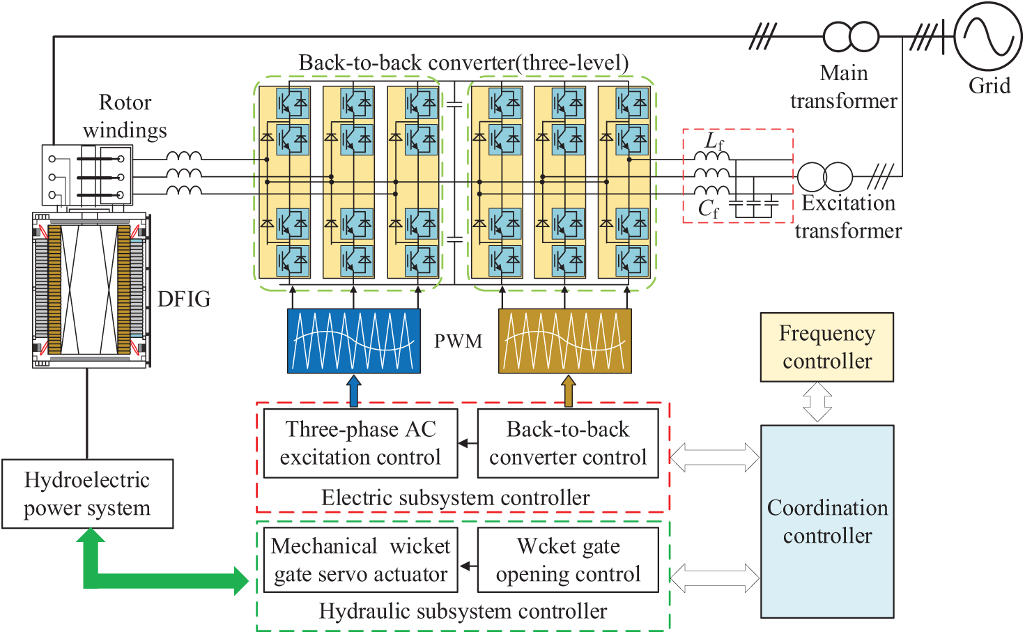
Figure 1: Structural diagram of DFVS-PSU
As a critical component of DFVS-PSUs, the excitation converter is essential for achieving high-efficiency energy conversion and stable grid integration. With the rated capacity of individual units now reaching the hundred-megawatt scale, converter systems face increasingly stringent requirements in terms of power capacity, voltage level, and output power quality. Compared to traditional two-level topologies, the NPC-TLC offers superior performance in terms of output voltage levels, harmonic distortion, voltage slew rate (du/dt), and scalability, making it an ideal solution for large-scale energy systems. Its structure is illustrated in Fig. 2.
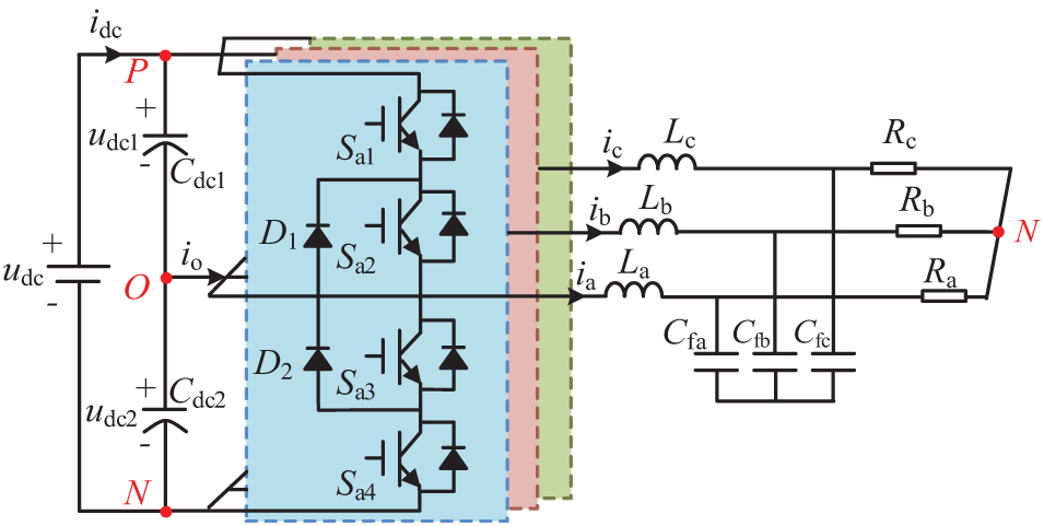
Figure 2: Topology of the NPC three-level excitation converter
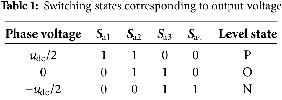
In the NPC-TLC topology, each phase (e.g., Phase A) consists of four power switches and two clamping diodes, designated as Sx1, Sx2, Sx3, Sx4 (x = a, b, c), D1 and D2, respectively. The correlation between the output voltage levels of Phase A and the switching states of the corresponding power switches is systematically outlined in Table 1, where ‘1’ represents the on-state and ‘0’ signifies the off-state of the switch.
As shown in Table 1, each phase of the NPC-TLC is capable of generating three voltage levels. Due to the independence of the three-phase outputs, the system can produce 27 distinct switching states, each uniquely corresponding to a space voltage vector. The magnitude and phase angle of each basic voltage vector can be calculated using Eq. (1). These space vectors are divided into six main sectors, as illustrated in Fig. 3.
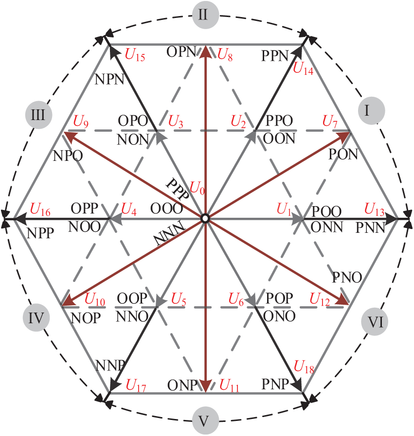
Figure 3: Space voltage vector of the NPC Three-Level excitation converter
3 Optimized Virtual Space Vector Pulse Modulation Strategy
3.1 Novel Voltage Vector Synthesis Rule
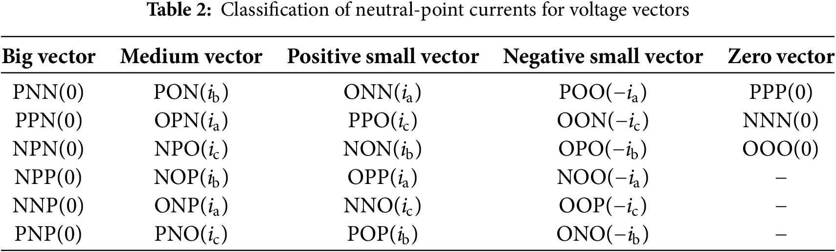
The synthesis of advanced virtual voltage vectors requires comprehensive consideration of three critical parameters: NPV regulation, CMV suppression, and switching state optimization. In NPC-TLC, the presence of a neutral-point current inevitably leads to fluctuations in the NPV, which may adversely affect system stability and performance. Therefore, effective suppression or elimination of the neutral-point current is essential to ensure NPV stabilization. Notably, different voltage vectors generate distinct neutral-point currents, the specific relationships of which are detailed in Table 2.
As with the neutral-point current, the magnitude of the CMV depends on the applied voltage vectors of the NPC three-level inverter, as expressed in Eq. (2).
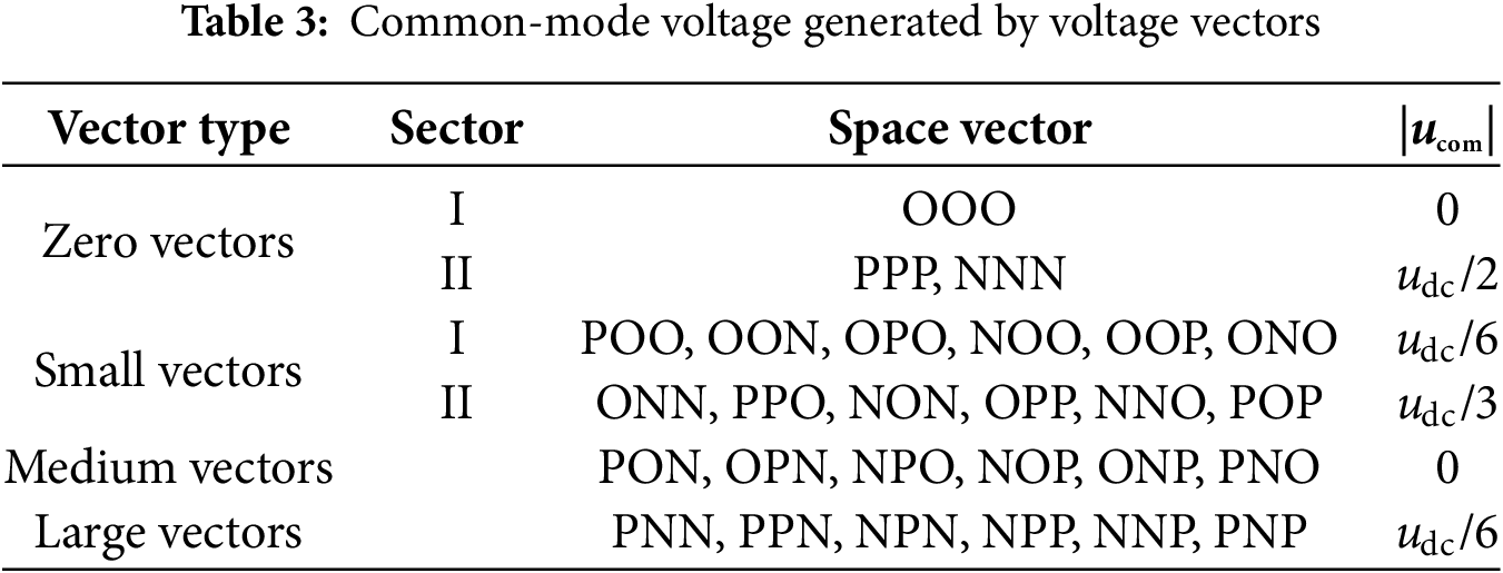
Let uao, ubo, uco denote the phase voltages at the output terminals of the converter. As derived from Eq. (2), the magnitude of the CMV exhibits a direct proportional relationship with the algebraic sum of the three-phase output voltages. To achieve CMV amplitude suppression, it is necessary to prioritize the selection of voltage vectors that result in lower phase voltage magnitudes. The corresponding CMV amplitudes associated with each space voltage vector, as calculated by Eq. (2), are systematically listed in Table 3.
According to the analysis above, the synthesis of novel virtual space voltage vectors requires holistic consideration of multiple performance metrics and must follow technical requirements:
1. NPV Regulation: The modulation scheme should ensure that the average neutral-point current over each fundamental carrier cycle is zero and exhibit robust dynamic regulation capability to effectively suppress fluctuations in the NPV, thereby enhancing system stability;
2. CMV Suppression: The synthesized virtual vectors must inherently suppress excessive CMV, minimizing detrimental effects on system electromagnetic compatibility and operational reliability;
3. Switching Actions Constraint: The proposed modulation approach should minimize the induction of significant increases in the switching actions of power semiconductor devices, thereby avoiding excessive switching losses and potential electromagnetic interference issues.
Consequently, the proposed strategy is required to effectively suppress CMV amplitude and accurately regulate NPV, while simultaneously optimizing the switching actions to enhance energy conversion efficiency and improve applicability in high-power scenarios. The synthesized virtual vectors within Sector I are illustrated in Fig. 4.
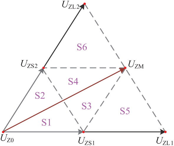
Figure 4: Virtual space voltage vectors in Sector I
The novel virtual small vector is mathematically defined in Eq. (3), and the associated neutral-point current generated within one carrier cycle is analytically characterized by Eq. (4).
The synthesis rules for the remaining novel virtual vectors are defined in Eq. (5).
The proposed strategy is implemented in the G-H coordinate system, with the duty cycles of virtual vectors for each subsector in Sector I shown in Table 4.
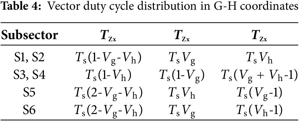
Specifically, Vg and Vh represent the projection components of the reference vector in the G–H coordinate system. In this coordinate system, all other main sectors can be rotated and mapped to Sector I to simplify the calculation process. Since the vector duty ratios in each Sector are completely consistent with those in Sector I, it is only necessary to calculate the virtual vector duty ratios for the subsectors within Sector I.
The proposed OVSVPWM strategy limits the CMV amplitude to udc/6 by eliminating high-CMV amplitude Type II small vectors and zero vectors, retaining only low-CMV Type I small vectors. Except for the novel virtual small vector, other virtual vectors do not generate a neutral-point current. Within a carrier cycle, if the three basic small vectors of the virtual small vector are applied for equal durations, the average neutral-point current is zero, ensuring NPV stability. Theoretically, this strategy achieves dynamic NPV balance and CMV suppression, enhancing system stability and reliability.
3.2 Control Strategy for Neutral-Point Voltage Stabilization
Theoretically, the proposed virtual space vector can achieve NPV balance within the modulation region. However, in practical operation, non-ideal factors such as dead-time effects, capacitance mismatches between the upper and lower DC-link capacitors, and parameter inconsistencies among switching devices may lead to NPV imbalance. Therefore, integrating an automatic NPV balancing mechanism into the proposed modulation strategy is essential to ensure stable system operation.
To quantitatively assess the extent of NPV fluctuations, the voltage fluctuation coefficients of the upper and lower capacitors are defined as Δu:
udc1 and udc2 represent the voltages of the upper and lower DC-link capacitors, respectively.
Space vectors of the NPC-TLC under different NPV fluctuation conditions are illustrated in Fig. 5.
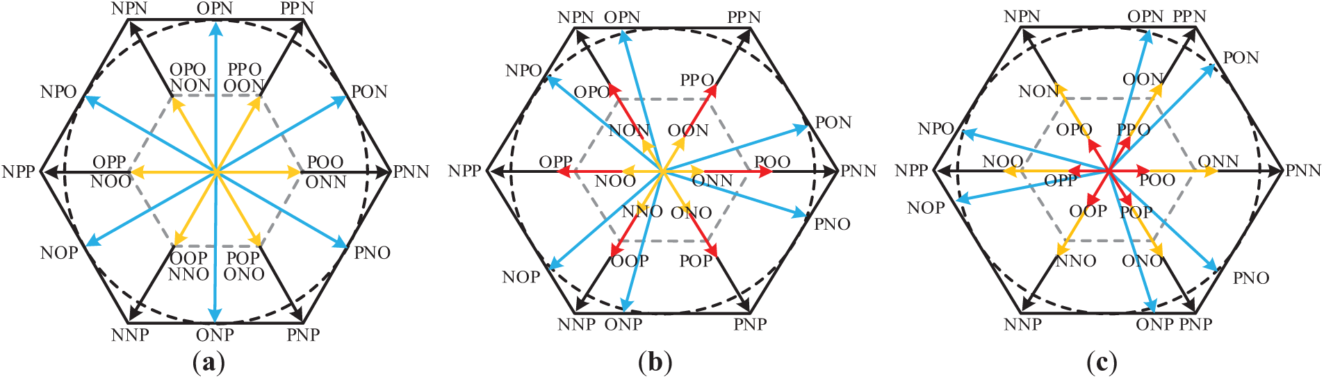
Figure 5: Characteristics of space vectors under different NPV fluctuation conditions: (a) Δu = 0; (b) Δu > 0; (c) Δu < 0
Therefore, excluding the proposed novel virtual small vector, the fundamental vectors constituting all other synthesized virtual vectors do not induce neutral-point current and are thus incapable of regulating NPV. By contrast, the novel virtual small vector—formed through the coordinated synthesis of three fundamental small vectors with distinct neutral-point current characteristics—exhibits an inherent capability for NPV regulation. This unique property renders it the essential mechanism for facilitating automatic NPV balancing within the proposed modulation framework.
Taking Sector I (S5) as an example, the virtual small vector Uzs1 is modulated by introducing a balancing factor k to achieve NPV balancing control, as described by the fundamental principle in Eq. (7).
The neutral-point current associated with the novel virtual small vector Uzs1 over a single carrier cycle is quantitatively described by Eq. (8).
Based on the derivations from Eqs. (3), (4), and (8), it can be concluded that the fundamental small vectors U6(ONO) and U2(OON) generate neutral-point currents of (−ib) and (−ic), respectively. According to the balanced three-phase current relationship, their combined neutral-point current is equivalent to ia. In contrast, the neutral-point current produced by U1(POO) is (−ia). This demonstrates that the neutral-point current induced by the novel virtual small vector Uzs1 depends solely on ia, as expressed in Eq. (8). Therefore, by appropriately adjusting the balancing factor k in real time to regulate the dwell times of constituent fundamental small vectors within the virtual small vector Uzs1, the neutral point current can be effectively controlled, thereby achieving automatic NPV balancing.
The specific value of the regulation balancing factor k can be calculated in real-time using Eq. (9).
where Ta is the conduction duration of phase current ia within a single carrier cycle, and C denotes the DC-link capacitance value.
To satisfy the volt-second balance principle, the valid range of the balancing factor k must be constrained. Based on real-time detection of NPV fluctuations Δu and phase current ix, the constraint conditions for the balancing factor k can be categorized into the following five cases:
1. When Δu = 0, it indicates that udc1 = udc2 and no NPV adjustment is required. Therefore, all vectors maintain equal duty cycles with the balancing factor k = 1/3;
2. When Δu > 0 and ia> 0, the condition udc1 > udc2 requires increasing the duty cycle of vector U1(POO) to discharge the upper capacitor voltage while charging the lower capacitor voltage, thereby achieving NPV balance. The valid range for the balancing factor k is (0, 1/3);
3. When Δu > 0 and ia < 0, the condition udc1 > udc2 requires decreasing the duty cycle of vector U1(POO) to discharge the upper capacitor voltage while charging the lower capacitor voltage, thereby achieving NPV balance. The valid range for the balancing factor k is (1/3, 1/2);
4. When Δu < 0 and ia > 0, the condition udc1 < udc2 requires decreasing the duty cycle of vector U1(POO) to charge the upper capacitor voltage while discharging the lower capacitor voltage, thereby achieving NPV balance. The valid range for the balancing factor k is (1/3, 1/2);
5. When Δu < 0 and ia < 0, the condition udc1 < udc2 requires increasing the duty cycle of vector U1(POO) to charge the upper capacitor voltage while discharging the lower capacitor voltage, thereby achieving NPV balance. The valid range for the balancing factor k is (0, 1/3).
Based on the preceding analysis, the automatic NPV balancing mechanism is illustrated in Fig. 6.
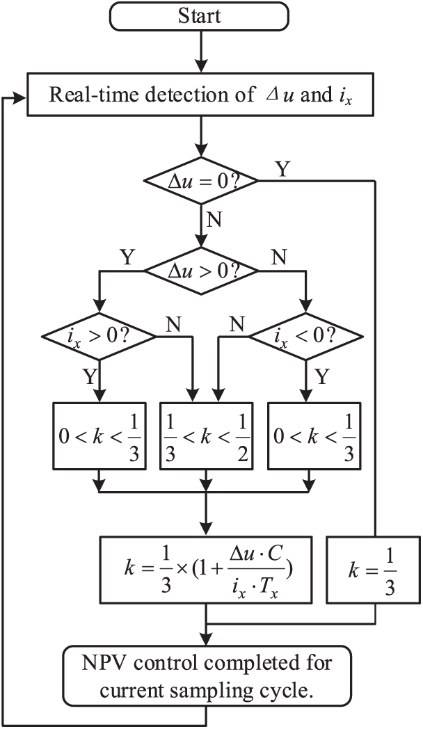
Figure 6: NPV automatic control flowchart
3.3 Optimization of Switching States
The control method proposed in this study can effectively stabilize the NPV across the entire modulation range. However, the original OVSVPWM strategy suffers from a significant increase in switching actions, compromising its practical applicability.
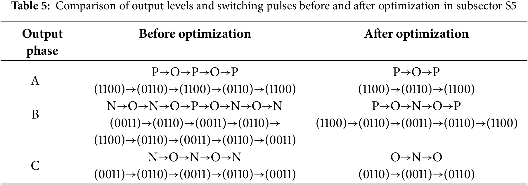
Taking the subsector S5 as an example, this study implements an optimized reconstruction of the switching-state sequence. Table 5 highlights the optimization effectiveness through detailed comparisons of three-phase level transition processes and switching pulse signals before and after optimization. The analysis reveals two primary issues in the unoptimized OVSVPWM strategy:
1. Increased switching actions: Before optimization, there are a total of 16 output-level transitions across the three phases, with each transition involving the turn-on or turn-off of two switching devices, resulting in a total of 32 switching actions.
2. Implementation difficulty: Before optimization, the three-phase output levels cannot achieve symmetrical output, making it impossible to implement the proposed strategy using traditional dual-modulation wave methods.
To address this, the phase duty ratio method is introduced. This method is predicated on the principle that, provided the switching duration of each phase remains invariant, the resultant impact on the three-phase converter output remains equivalently unaltered.
Based on this principle, the specific process for switching state optimization is as follows: first, the durations of identical output levels for each phase within one carrier cycle in Fig. 7a are accumulated. Then, the traditional double-pulse modulation method is employed to sequentially output the rearranged switching states in the order of P→O→N. The optimized sequence is shown in Fig. 7b. The optimized switching states yield symmetrical output, reduce implementation complexity, and limit the number of level transitions per carrier cycle to 8, thereby reducing the number of switching actions by 16, as illustrated in Fig. 7 and Table 5. Although the sequence of output levels is rearranged, their respective durations remain unchanged. Thus, the output performance of the converter is not compromised. The optimized switching states corresponding to each subsector within Sector I are shown in Fig. 8.
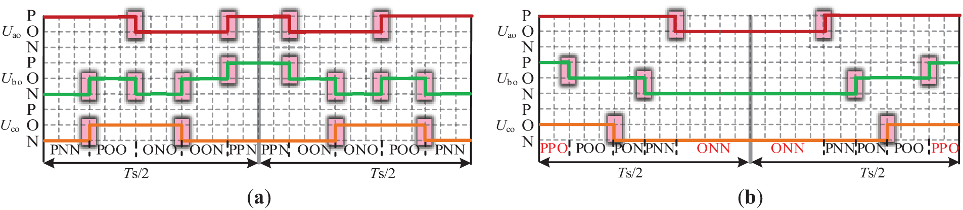
Figure 7: Switching state optimization in a carrier cycle: (a) Before optimization; (b) After optimization
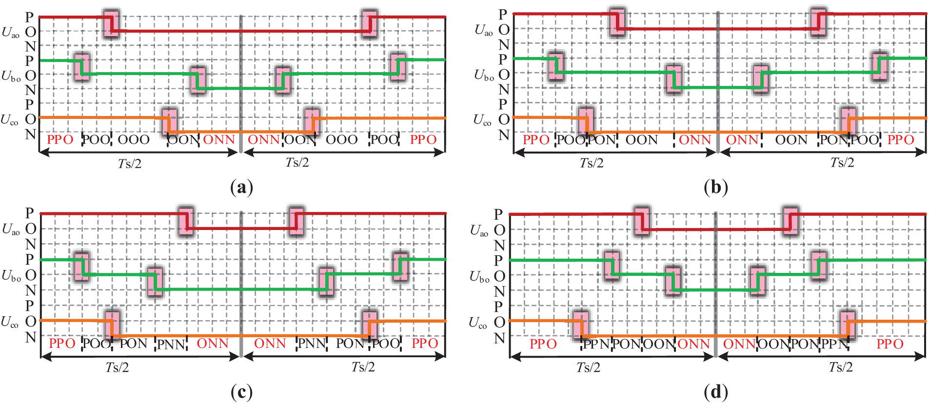
Figure 8: Optimized switching state for each subsector within Sector I: (a) S1 and S2; (b) S3 and S4; (c) S5; (d) S6
3.4 Common-Mode Voltage Suppression
The initial modulation strategy exclusively utilizes Type I small vectors, characterized by minimal CMV amplitude, to effectively suppress CMV. However, during the switching state optimization process, certain Type II small vectors with relatively higher CMV amplitudes—such as [PPO] and [ONN]—are reintroduced, resulting in a marked increase in CMV magnitude, as illustrated in Fig. 8. Consequently, even after achieving NPV balance and switching sequence optimization, the issue of CMV suppression remains to be addressed.
As shown in Fig. 8, Type-II small vectors are typically composed of two phases with identical non-zero voltage levels and one phase at the zero level (e.g., PPO, ONN). To completely eliminate the influence of Type-II small vectors and achieve CMV suppression, it is necessary to avoid the superposition of identical non-zero voltage levels in two phases. Taking subsector S5 in Sector I as an example, the output level sequence of phase B is modified from P→O→N to N→O→P, thereby preventing the overlap of two non-zero phase levels. The specific process of Phase B output level inversion is as follows:
1. Assume the original dual modulation waves of Phase B are mb1 and mb2, as shown in Fig. 9a. Their complementary modulation waves are calculated as mb11 = Ts − mb1 and mb22 = Ts − mb2, shown in Fig. 9b. All phase modulation waveforms are computed within the DSP.
2. The calculated modulation signals for each phase are transferred from the DSP to the FPGA via the address bus and compared with the carrier signal. The comparison results between the Phase B modulation signals and the carrier are illustrated in Fig. 9b. After comparing the complementary modulation signals of Phase B with the carrier, the pulse state 1100 maintains the same effective duration as the original N-level, 1001 corresponds to the original O-level duration, and 0011 matches the original P-level duration. This step is implemented within the FPGA.
3. The final output pulses of Phase B undergo logical inversion within the FPGA, as illustrated in Fig. 9c.
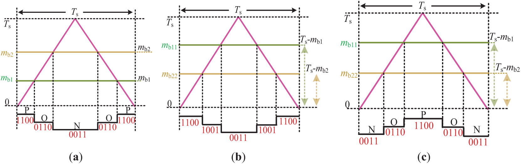
Figure 9: Phase B level inversion principle: (a) Before optimization; (b) Transition state; (c) After optimization
Based on the above analysis, while the proposed strategy’s switching-state output exhibits greater complexity compared to conventional modulation methods, this complexity is solely reflected in software implementation. The strategy can be fully realized using standard converter hardware platforms incorporating DSP + FPGA architectures. Therefore, it does not significantly increase equipment costs.
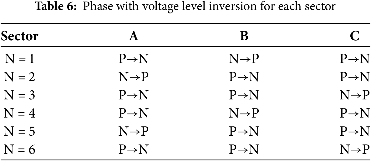
The phase corresponding to level inversion in each major Sector is detailed in Table 6.
In Fig. 10, the P and N states of each phase are interleaved, with the O state acting as a buffer, effectively preventing the generation of Type II small vectors. Since Type I small vectors are used to synthesize virtual vectors, each phase naturally passes through the O state between P and N within a single sampling period. This ensures that non-zero switching states do not occur simultaneously across phases, as transitions between P and N are mediated solely by O, inherently eliminating Type II small vectors and significantly reducing CMV.
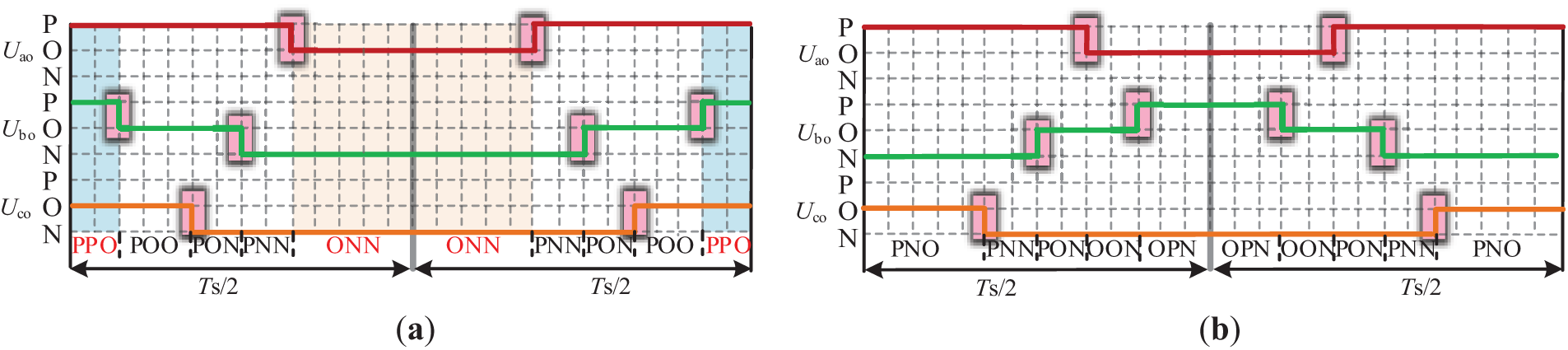
Figure 10: Optimized switching sequence for CMV suppression: (a) Before optimization; (b) After optimization
According to the principle of the phase voltage duty ratio method, as long as the duty ratios of each phase voltage level remain unchanged before and after adjustment, the effect of the three-phase output voltage on the converter remains equivalent within a single carrier cycle. Therefore, the previously proposed strategy—dynamically adjusting the duty ratio of the virtual small vector to achieve autonomous NPV regulation—remains effective without compromising output performance.
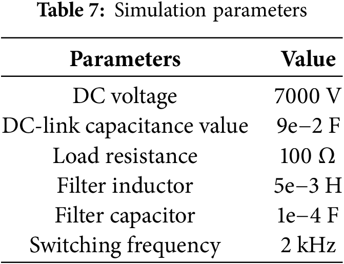
The NPC-TLC system was simulated in MATLAB/Simulink, with specific parameters listed in Table 7. In this study, various modulation indices (MI) were selected to perform a comparative analysis of output performance indicators among several mainstream space vector pulse width modulation strategies, including the space vector pulse width modulation (SVPWM), the TVSVPWM, and the OVSVPWM.
As shown in Fig. 11, both modulation strategies enable the NPC-TLC system to produce stable outputs. The phase voltage, line voltage, and phase current waveforms are regular and sinusoidal, indicating normal system operation.
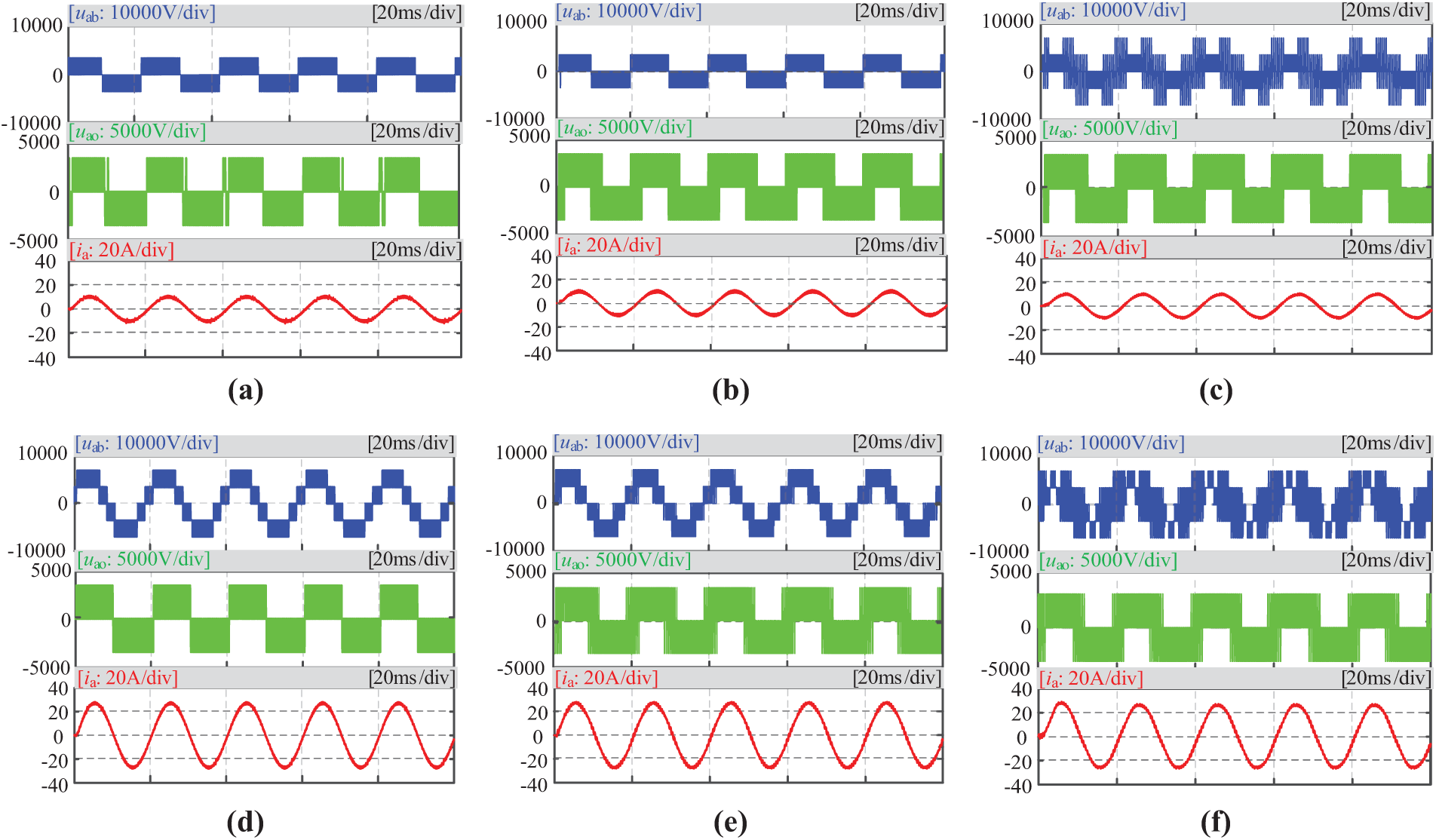
Figure 11: Three modulation strategies’ steady-state output waveforms (a) SVPWM, MI = 0.3; (b) TSVPWM, MI = 0.3; (c) OVSVPWM, MI = 0.3; (d) SVPWM, MI = 0.8. (e) TVSVPWM, MI = 0.8; (f) OVSVPWM, MI = 0.8
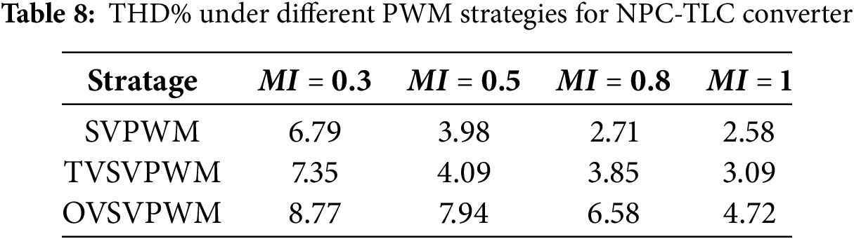
The comparison of THD under different PWM strategies is shown in Table 8. Due to the use of more basic vectors in constructing virtual vectors, the THD% of the OVSVPWM strategy is higher than that of the SVPWM and TVSVPWM strategies. However, it remains within an acceptable range.
As shown in Fig. 12, significant differences exist in the amplitude of CMV among the three modulation strategies. When using SVPWM and TVSVPWM, the output CMV amplitude reaches 2333.3 V(udc/3). In contrast, the OVSVPWM strategy reduces the CMV amplitude to 1166.6 V(udc/6), which is only half that of SVPWM and TVSVPWM. These results clearly demonstrate the superior performance of the OVSVPWM strategy in suppressing CMV amplitude, effectively mitigating the impact of CMV on the system, and enhancing electromagnetic compatibility and operational reliability.
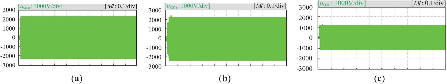
Figure 12: Output CMV amplitudes of SVPWM, TVSVPWM, and OVSVPWM strategies over the full MI (a) SVPWM; (b) TVSVPWM; (c) OVSVPWM
To verify the effectiveness of the proposed strategy in suppressing CMV amplitude, the CMV RMS values of the three modulation strategies over the full modulation range are shown in Fig. 13.
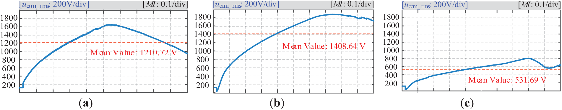
Figure 13: RMS of CMV under three modulation strategies over the full MI (a) SVPWM; (b) TVSVPWM; (c) OVSVPWM
As shown in Fig. 13, the proposed strategy achieves the lowest root mean square (RMS) value of CMV across the entire MI range, with an average of merely 531.69 V. In comparison, the average RMS values for SVPWM and TVSVPWM reach 1210.72 and 1408.64 V, respectively, which fully demonstrates the superior performance of the proposed strategy in CMV amplitude suppression.
Similarly, to verify the effectiveness of the proposed strategy in NPV control, simulations were conducted to evaluate the NPV fluctuations of the three modulation strategies across the full MI range. As shown in Fig. 14, the results demonstrate that while all three modulation strategies can effectively control NPV throughout the modulation range, the proposed OVSVPWM strategy delivers superior performance in NPV control.
Figure 14: Output NPV amplitudes of SVPWM, TVSVPWM, and OVSVPWM strategies over the full MI (a) SVPWM; (b) TVSVPWM; (c) OVSVPWM
To further verify the dynamic NPV control performance of the three modulation strategies, simulations were conducted with the DC-side capacitors initially set to asymmetric voltages (udc1 = 3600 V, udc2 = 3400 V), and NPV control was activated at t = 1 s. As shown in Fig. 15, all three strategies achieve dynamic NPV balancing, but there are significant differences in convergence speed under high modulation indices. Notably, while SVPWM and TVSVPWM maintain a constant CMV amplitude of 2333.3 V (udc/3), the OVSVPWM strategy successfully suppresses the CMV amplitude to 1166.6 V(udc/6) while achieving faster NPV balancing. These results conclusively demonstrate OVSVPWM’s dual advantages in both dynamic voltage regulation and CMV amplitude suppression.
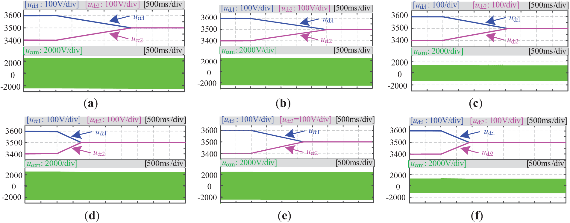
Figure 15: Dynamic response of NPV and CMV (a) SVPWM, MI = 0.3; (b) TVSVPWM, MI = 0.3; (c) OVSVPWM, MI = 0.3; (d) SVPWM, MI = 0.8; (e) TVSVPWM, MI = 0.8; (f) OVSVPWM, MI = 0.8
To evaluate the dynamic performance of the three modulation strategies under varying load conditions, Fig. 16 presents the transient characteristics of NPV, ia, and CMV when the resistive load undergoes a step change from 100 Ω to 50 Ω. The results demonstrate that while all three strategies maintain a normal output of voltage and current during load transients, the proposed OVSVPWM strategy exhibits superior NPV regulation capability and lower CMV amplitude (limited to udc/6). These findings further validate the effectiveness and advantages of OVSVPWM in practical operating conditions.
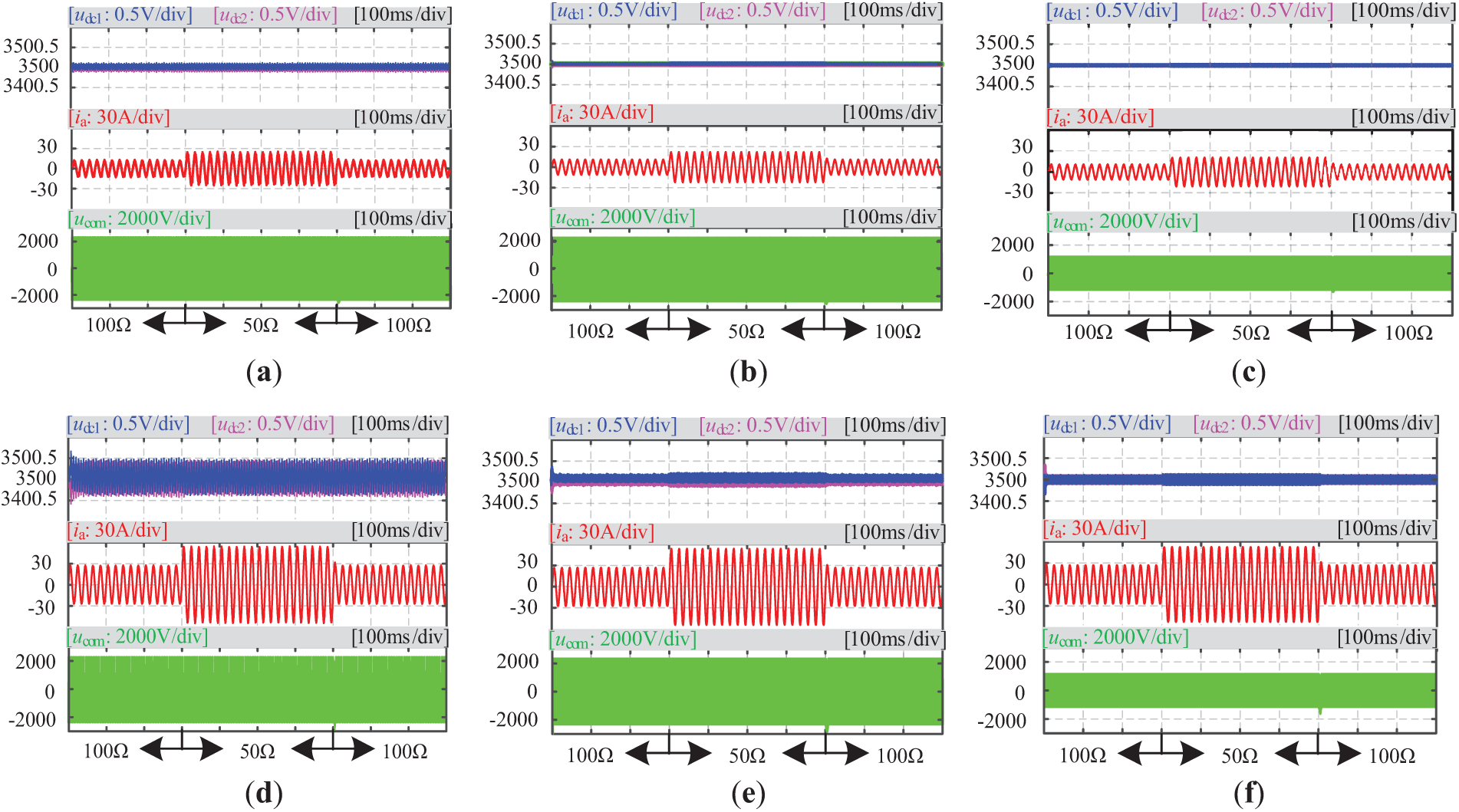
Figure 16: Simulation results of NPV, ia, and CMV during load variation (a) SVPWM, MI = 0.3; (b) TVSVPWM, MI = 0.3; (c) OVSVPWM, MI = 0.3; (d) SVPWM, MI = 0.8. (e) TVSVPWM, MI = 0.8; (f) OVSVPWM, MI = 0.8
This paper proposes an optimized OVSVPWM strategy aimed at addressing the issues of excessive CMV amplitude and NPV balancing control in the NPC-TLC topology of doubly fed wind power systems. The strategy introduces a real-time feedback mechanism to adjust the balancing factor dynamically, achieving self-balancing control of the NPV. To overcome the increased switching actions and implementation complexity brought by this strategy, a switching sequence optimization method based on phase duty ratio is employed, combined with a zero-level buffering technique to effectively suppress CMV amplitude and reduce switching losses. Simulation results demonstrate that, compared with conventional modulation strategies, this method significantly improves system performance by effectively suppressing NPV fluctuations, limiting the CMV amplitude within udc/6, and enhancing overall system efficiency, showing strong engineering practicality and application potential.
Acknowledgement: Not applicable.
Funding Statement: The authors received no specific funding for this study.
Author Contributions: The authors confirm their contribution to the paper as follows: study conception and design: Ziqiang Man, Lei Zhao; data collection: Zheng Tao, Shiming Cheng; analysis and interpretation of results: Ziqiang Man, Lei Zhao, Zheng Tao, Shiming Cheng, Wei Yan, Li Zhang. Draft manuscript preparation: Gaoyue Zhong, Yu Lu, Wenming Zhang, and final revision and proofreading: Wenming Zhang, Li Zhang. All authors reviewed the results and approved the final version of the manuscript.
Availability of Data and Materials: The data that support the findings of this study are available from the corresponding author upon reasonable request.
Ethics Approval: Not applicable.
Conflicts of Interest: The authors declare no conflicts of interest to report regarding the present study.
References
1. Fan J, Niu L, Li C, Zhang G, Li H, Wang Y, et al. Review of black start on new power system based on energy storage technology. Energ Eng. 2023;120(12):2857–78. doi:10.32604/ee.2023.029740. [Google Scholar] [CrossRef]
2. Chen Y, Xu W, Liu Y, Bao Z, Mao Z, Rashad EM. Modeling and transient response analysis of doubly-fed variable speed pumped storage unit in pumping mode. IEEE Trans Ind Electron. 2023;70(10):9935–47. doi:10.1109/TIE.2022.3224154. [Google Scholar] [CrossRef]
3. Chen Y, Deng C, Zhao Y. Coordination control between excitation and hydraulic system during mode conversion of variable speed pumped storage unit. IEEE Trans Power Electron. 2021;36(9):10171–85. doi:10.1109/TPEL.2021.3061268. [Google Scholar] [CrossRef]
4. Alsofyani IM, Lee KB. Simple capacitor voltage balancing for three-level NPC inverter using discontinuous PWM method with hysteresis neutral-point error band. IEEE Trans Power Electron. 2021;36(11):12490–503. doi:10.1109/TPEL.2021.3074957. [Google Scholar] [CrossRef]
5. Desingu K, Selvaraj R, Chelliah TR, Khare D. Effective utilization of parallel-connected megawatt three-level back-to-back power converters in variable speed pumped storage units. IEEE Trans Ind Appl. 2019;55(6):6414–26. doi:10.1109/TIA.2019.2936365. [Google Scholar] [CrossRef]
6. Leon JI, Kouro S, Franquelo LG, Rodriguez J, Wu B. The essential role and the continuous evolution of modulation techniques for voltage-source inverters in the past, present, and future power electronics. IEEE Trans Ind Electron. 2016;63(5):2688–701. doi:10.1109/TIE.2016.2519321. [Google Scholar] [CrossRef]
7. Zorig A, Barkat S, Sangwongwanich A. Neutral point voltage balancing control based on adjusting application times of redundant vectors for three-level NPC inverter. IEEE J Emerg Sel Top Power Electron. 2022;10(5):5604–13. doi:10.1109/JESTPE.2022.3186927. [Google Scholar] [CrossRef]
8. Nadh G, Rahul SA. Clamping modulation scheme for low-speed operation of three-level inverter fed induction motor drive with reduced CMV. IEEE Trans Ind Appl. 2022;58(6):7336–45. doi:10.1109/TIA.2022.3199193. [Google Scholar] [CrossRef]
9. Das D, Weise N, Basu K, Baranwal R, Mohan N. A bidirectional soft-switched DAB-based single-stage three-phase AC–DC converter for V2G application. IEEE Trans Transp Electrific. 2019;5(1):186–99. doi:10.1109/TTE.2018.2886455. [Google Scholar] [CrossRef]
10. Xiong W, Sun Y, Su M, Zhang J, Liu Y, Yang J. Carrier-based modulation strategies with reduced common-mode voltage for five-phase voltage source inverters. IEEE Trans Power Electron. 2018;33(3):2381–94. doi:10.1109/TPEL.2017.2692778. [Google Scholar] [CrossRef]
11. Xia S, Wu X, Zheng J, Li X, Wang K. A virtual space vector PWM with active neutral point voltage control and common mode voltage suppression for three-level NPC converters. IEEE Trans Ind Electron. 2021;68(12):11761–71. doi:10.1109/TIE.2020.3048292. [Google Scholar] [CrossRef]
12. Lak M, Tsai YT, Chuang BR, Lee TL, Moradi MH. A hybrid method to eliminate leakage current and balance neutral point voltage for photovoltaic three-level T-type inverter. IEEE Trans Power Electron. 2021;36(10):12070–89. doi:10.1109/TPEL.2021.3073471. [Google Scholar] [CrossRef]
13. Zhao Z, Zhong Y, Gao H, Yuan L, Lu T. Hybrid selective harmonic elimination PWM for common-mode voltage reduction in three-level neutral-point-clamped inverters for variable speed induction drives. IEEE Trans Power Electron. 2012;27(3):1152–8. doi:10.1109/TPEL.2011.2162591. [Google Scholar] [CrossRef]
14. Yao J, Chen W, Xue C, Yuan Y, Wang T. An ISOP hybrid DC transformer combining multiple SRCs and DAB converters to interconnect MVDC and LVDC distribution networks. IEEE Trans Power Electron. 2020;35(11):11442–52. doi:10.1109/TPEL.2020.2983954. [Google Scholar] [CrossRef]
15. Li C, Yang T, Kulsangcharoen P, Calzo GL, Bozhko S, Gerada C, et al. A modified neutral point balancing space vector modulation for three-level neutral point clamped converters in high-speed drives. IEEE Trans Ind Electron. 2019;66(2):910–21. doi:10.1109/TIE.2018.2835372. [Google Scholar] [CrossRef]
16. Wang C, Li Y. Analysis and calculation of zero-sequence voltage considering neutral-point potential balancing in three-level NPC converters. IEEE Trans Ind Electron. 2010;57(7):2262–71. doi:10.1109/TIE.2009.2024093. [Google Scholar] [CrossRef]
17. Celanovic N, Boroyevich D. A Comprehensive study of neutral-point voltage balancing problem in three-level neutral-point-clamped voltage source PWM inverters. IEEE Trans Power Electron. 2000;15(2):242–49. doi:10.1109/63.838096. [Google Scholar] [CrossRef]
18. Lewicki A, Krzeminski Z, Abu-Rub H. Space-vector pulsewidth modulation for three-level NPC converter with the neutral point voltage control. IEEE Trans Ind Electron. 2011;58(11):5076–86. doi:10.1109/TIE.2011.2119453. [Google Scholar] [CrossRef]
19. Zhou D, Jiang C, Quan Z, Li YR. Vector shifted model predictive power control of three-level neutral-point-clamped rectifiers. IEEE Trans Ind Electron. 2020;67(9):7157–66. doi:10.1109/TIE.2019.2946549. [Google Scholar] [CrossRef]
20. Tang Y, Xu W, Dong D, Liu Y, Ismail MM. Low-complexity multistep sequential model predictive current control for three-level inverter-fed linear induction machines. IEEE Trans Ind Electron. 2023;70(6):5537–48. doi:10.1109/TIE.2022.3192688. [Google Scholar] [CrossRef]
21. Lopez I, Ceballos S, Pou J, Zaragoza J, Andreu J, Ibarra E, et al. Generalized PWM-based method for multiphase neutral-point-clamped converters with capacitor voltage balance capability. IEEE Trans Power Electron. 2017;32(6):4878–90. doi:10.1109/TPEL.2016.2599872. [Google Scholar] [CrossRef]
22. Xia C, Shao H, Zhang Y, He X. Adjustable proportional hybrid SVPWM strategy for neutral-point-clamped three-level inverters. IEEE Trans Ind Electron. 2013;60(10):4234–42. doi:10.1109/TIE.2012.2213558. [Google Scholar] [CrossRef]
23. Jiang D, Chen J, Shen Z. Common mode EMI reduction through PWM methods for three-phase motor controller. CES Trans Electr Mach Syst. 2019;3(2):133–42. doi:10.30941/CESTEMS.2019.00019. [Google Scholar] [CrossRef]
24. Ma B, Xu X, Wang K, Zheng Z, Li Y. A neutral-point potential balancing method for a three-level neutral-point-clamped back-to-back converter. In: Proceedings of the 2019 IEEE Transportation Electrification Conference and Expo, Asia-Pacific (ITEC Asia-Pacific); 2019 May 8–10; Seogwipo, Republic of Korea. Piscataway, NJ, USA: IEEE; 2019. p. 1–5. [Google Scholar]
Cite This Article
 Copyright © 2025 The Author(s). Published by Tech Science Press.
This work is licensed under a Creative Commons Attribution 4.0 International License , which permits unrestricted use, distribution, and reproduction in any medium, provided the original work is properly cited.
 Downloads
 Citation Tools