
 Submit a Paper
 Propose a Special lssue
 Open Access
ARTICLE

Experimental Evaluation of the Static and Dynamic Electrical Parameters of the Solar Panels to Characterize Their Real-Time Performance at Variable Operational Conditions
School of Engineering, Computing and Mathematics, University of Plymouth, Plymouth, UK
* Corresponding Author: Tamer Kamel. Email:
(This article belongs to the Special Issue: Recent Advance and Development in Solar Energy)
Energy Engineering 2026, 123(4), 1 https://doi.org/10.32604/ee.2026.078417
Received 30 December 2025; Accepted 11 February 2026; Issue published 27 March 2026
 View Full Text
 Download PDF
Abstract
This study provides a new experimental framework to measure the static and dynamic electrical parameters for a solar panel of multiple cells. The study evaluates its static parameters, including its resultant diodes’ saturation currents, diodes’ ideality factors, series, and shunt resistances. Such parameters are essential to characterise the steady-state performance of a solar panel. Additionally, the dynamic parameters as the equivalent junction and diffusion capacitances are also experimentally measured. These parameters impact the performance of the panel at variable solar irradiance, temperature, and load conditions. A solar panel of 36 series-connected cells has been utilised in this research to undertake this experimental evaluation. This work addresses a gap in the recent literature regarding a full evaluation of the internal electrical parameters in a whole solar panel of multiple cells. Firstly, a dark experimental environment has been developed so that no influence from external light sources can affect the measurements being taken. The panel is then stimulated with different types of electrical stresses in various circuit configurations to measure the required static and dynamic parameters. For the solar panel under study, the series and shunt resistances per cell have been evaluated to be 18.91 mΩ and 5.6 kΩ, respectively, while the junction and diffusion capacitances have shown direct and inverse relationships, respectively, with the applied voltage as expected. The outcomes of these experimental setups highlighted the importance of the developed comprehensive framework in this research to be employed to assess the quality of the solar panel and its real-time performance at variable operational conditions.Keywords
Sunlight is a spectrum of photons distributed over a range of energy. The electrons can be excited and move from the valence to the conduction band by photons whose energy is greater than the band gap energy, this being the energy required to jump the gap between the valence band and the conduction band. Here, they can exit the device and can then be used to generate electrical power in an external circuit. The photons which have an energy level that is less than the energy gap do not excite free electrons, this energy moves through the solar cell and is absorbed as heat in the back of the module. A metallic grid on the top side of the PV module forms one of the electrical contacts to the diode which allows light to fall onto the panel between the gridlines which is then absorbed into the material to be converted into electrical energy. An antireflective layer between the gridlines increases the transmission of light into the semiconductor material [1].
A Photovoltaic (PV) device is an element that converts sunlight into electricity. The basic PV device is the PV cell. A set of connected cells form a panel or module. Panels are generally composed of a series of cells in order to obtain a larger output voltage. Panels with large output currents are achieved by increasing the surface area of the cells or by connecting the cells in parallel. A photovoltaic array may be either a panel or a set of panels connected in series or parallel to form a large PV system.
Solar materials are chosen largely on how well their absorption characteristics match the solar spectrum. Another limiting factor is the cost of fabrication. Silicon is a common choice of material used to manufacture PV panels due to the materials absorption characteristics being a relatively good match to the solar spectrum; and silicon fabrication is well developed in the semiconductor electronics industry. Electronic grade semiconductors are extremely pure crystalline materials whose crystalline nature means that atoms are aligned in a regular periodic array. This periodicity, coupled with the atomic properties of the component elements is what gives semiconductors their useful electronic properties. However, under real operation conditions, it is apparent that the specifications provided by the manufacturers of commercial panels are not a true representation of how PV panels may behave when deployed in the field [2].
A PV cell is simply a semiconductor current rectifier, or diode with a photogenerated current source. The IV characteristics of this circuit is given in the Shockley solar cell equation [3].
where
The double-diode model (DDM), as illustrated in Fig. 1, describes the PN junction operation through the Shockley equation, and includes series and shunt resistances to incorporate the current-dependent and the voltage-dependent loss mechanisms. It has the important feature of modelling the carrier-recombination losses in the depletion region [4].
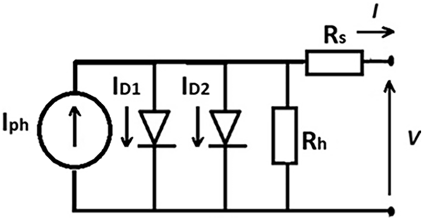
Figure 1: The two-diode model equivalent circuit.
The non-linear equation giving the relationship between the current and the voltage at the PV source terminals is:
The photocurrent (
On the other hand, the capacitance of the PV cell can be broken down into two different types, junction or barrier capacitance Cj which consists of mobile carriers in the depletion region and diffusion capacitance Cd which is attributed to the minority charge carriers in the bulk material. One is often referred to as low voltage capacitance (Cj) and the other a high voltage capacitance Cd. They are both dependant on the applied voltage, which allows combining the two into the strongly voltage dependent free carrier capacitance as discussed in [5]. PV cells using silicon-based technology tend to have the junction capacitance as the dominant capacitance at low voltages of (
Additionally, various recent research approaches have investigated the different parameters that could affect the performance of the solar cells and their qualities. Papers [7,8] have explored the output power factor (PF) and total harmonic distortion (THD) of the solar panels at different irradiance conditions. Other research [9,10] has provided experimental evaluation of the solar panels as a Photovoltaic/Thermal System, where the panel acts as a source of electric and heat energies. Nevertheless, all these papers have evaluated the solar panels by only assessing their output electrical measurements including, their output voltage, current and power without deepening into their internal static and dynamic parameters.
On the other hand, other research papers have evaluated some of these internal parameters in the individual solar cells using different approaches of machine learning techniques. Paper [11] used only the one-diode model to represent the solar cell and has simply combined the two capacitance types together into one bulk parameter.
Other papers employed machine learning approaches to estimate these internal parameters in individual cells such as teaching-learning-based optimisation algorithms undertaken in [12], particle swarm optimization algorithm in [13], and Laplacian Nelder-Mead spherical evolution in [14]. However, they all investigated only the static parameters of the individual solar cells without insights on their dynamic parameters including the diffusion and junction capacitances and how to distinctively estimate them.
In view of that, the novelty of this paper is emphasised as it provides a comprehensive experimental framework to evaluate the whole static and dynamic parameters of a full PV panel of 36 series-connected PV cells. Such a full framework has not been presented before in the literature for PV panels. The paper measures the static parameters of the PV panel including the overall equivalent two diodes’ saturation currents, the two diodes’ ideality factors, and the series and shunt resistances. The paper then evaluates the dynamic parameters including the overall resultant junction and diffusion capacitances of the panel. These static and dynamic parameters govern the performance of the PV panel and assess its characteristics and qualities at different operational conditions. Accordingly, the main contributions of this paper can be demonstrated as follows:
1. This paper presents for the first time a new comprehensive experimental evaluation for the static and dynamic parameters of a whole solar panel of multiple connected cells not of a single cell as has been provided in the state-of-the-art literature in this research scope.
2. Furthermore, this paper provides a full parameters’ estimation of the solar panel including the two-diode model of its solar cells, their series and shunt resistances as well as their junction and diffusion capacitances. Where all the previous and recent research has only focused on a few aspects of these parameters and not all of them.
3. Moreover, this paper establishes three different experimental setups to deduce the various required electrical parameters of the solar panel. Each experimental setup has been uniquely designed and developed to capture the corresponding electrical parameters under the proper and correct electrical and biasing conditions informed by literature in this research area.
The remainder of the paper is organized as follows. Section 2 demonstrates the experimental procedures for evaluating the static parameters of the PV panel at dark conditions. Then the dynamic parameters are measured in Section 3 using two unique experimental setups one for each capacitance type. Eventually, conclusions and discussions of the developed results are highlighted in Section 4.
2 Evaluation of a PV Panel’s Static Parameters at Dark Conditions
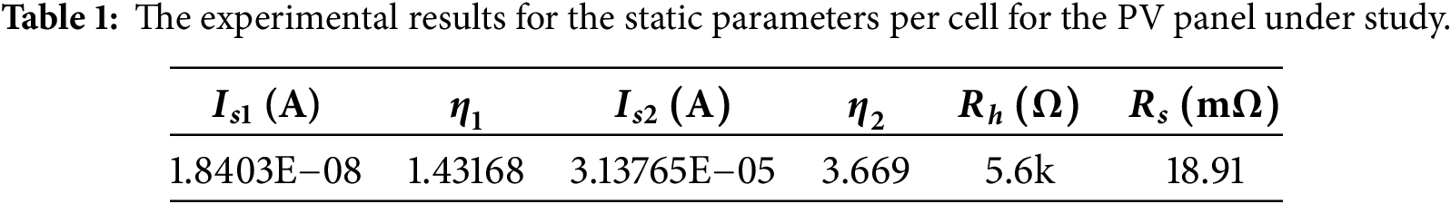
To conduct the dark experimental measurements of the PV panel, a dark environment is created so that no influence from external light sources, including ambient day light, can affect the measurements being taken. The panel is then externally supplied with electrical sources meaning that no light source is required to stimulate the panel. Fig. 2 illustrates the construction of the box to enclose the panel to undertake the required tests. The schematic of the circuit used for the experiments is demonstrated in Fig. 3. The specifications sheet of the 10 W commercial PV panel under study stated a maximum supply current of 0.6 A, so a safe limit was set at 0.5 A along with a maximum voltage limit of 40 V to ensure that the panel would not be damaged. The external resistance (R) is chosen to be 47 Ω. The experiment was started at 0 volts and was increased in 0.1-V steps and the corresponding current measured in microamps so that no information was lost. The resulting measurements were then used to generate the plot developed in Fig. 4. The developed plot is divided into the higher-values portion to extract the Rs and first diode Is1 and η1. While the lower-values portion is then used to extract the Rh and second diode Is2 and η2.
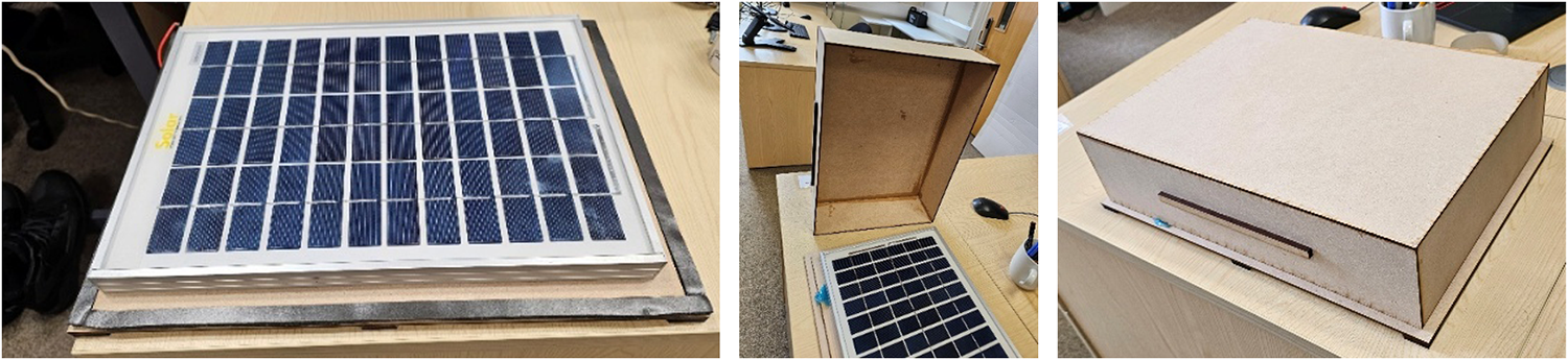
Figure 2: Dark experimental setup for the PV panel under study.
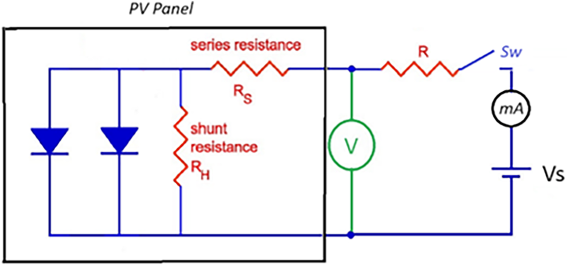
Figure 3: Dark experimental setup for the PV panel under study.
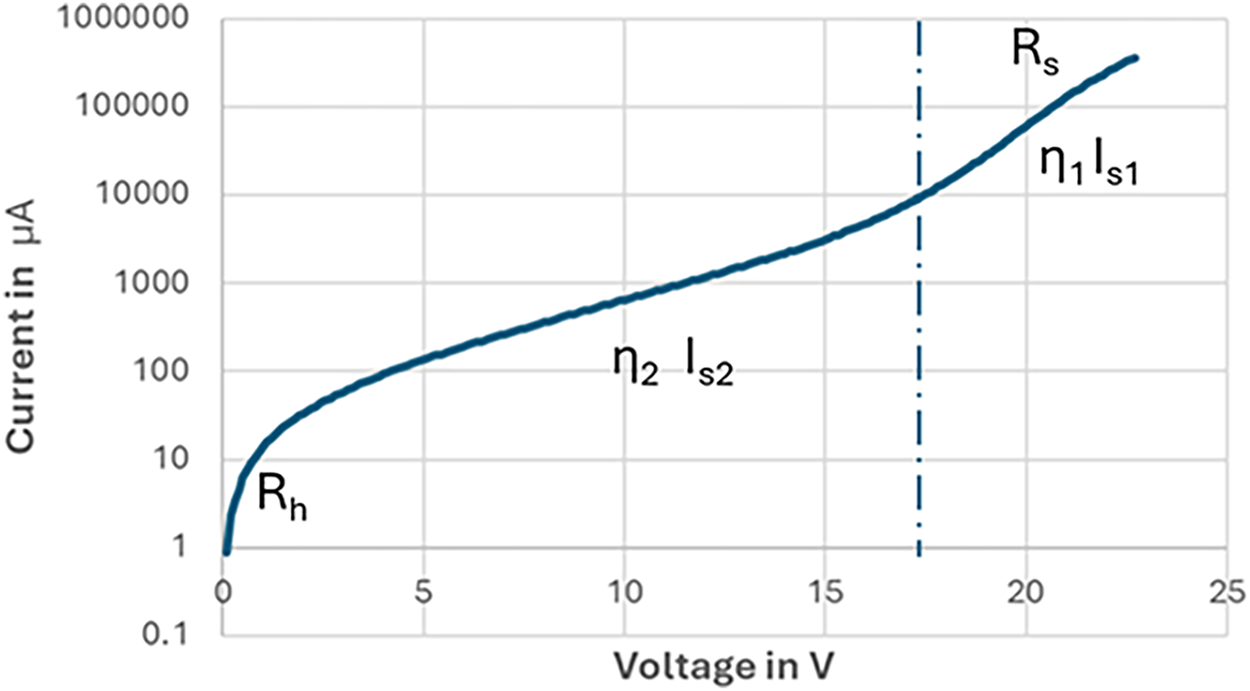
Figure 4: the PV panel’s I-V characterises to extract the panel static parameters.
Fig. 4 shows a resemblance to the plot of [15] but this being for a single PV cell, where the regions of higher and lower I-V values are also identified to evaluate the static parameters associated to each region. On the other hand, to take into account the 36 series-connected PV cells in the panel under study, the equivalent circuit diagram for the connected cells has to be deduced at each region to facilitate the calculation of the required parameters per cell in this research. Fig. 5 demonstrates the equivalent circuit diagram of the PV panel at dark conditions, where the 36 cells are connecting in series across their external contacts. Consequently, at lower I-V values, both diodes in each cell would be turning off allowing the current to flow only through their Rs and Rh resistances as illustrated in Fig. 6. Conversely, at higher I-V values, both diodes of each cell would be acting as a short wire across their Rh. Fig. 7 shows such a circuit arrangement.
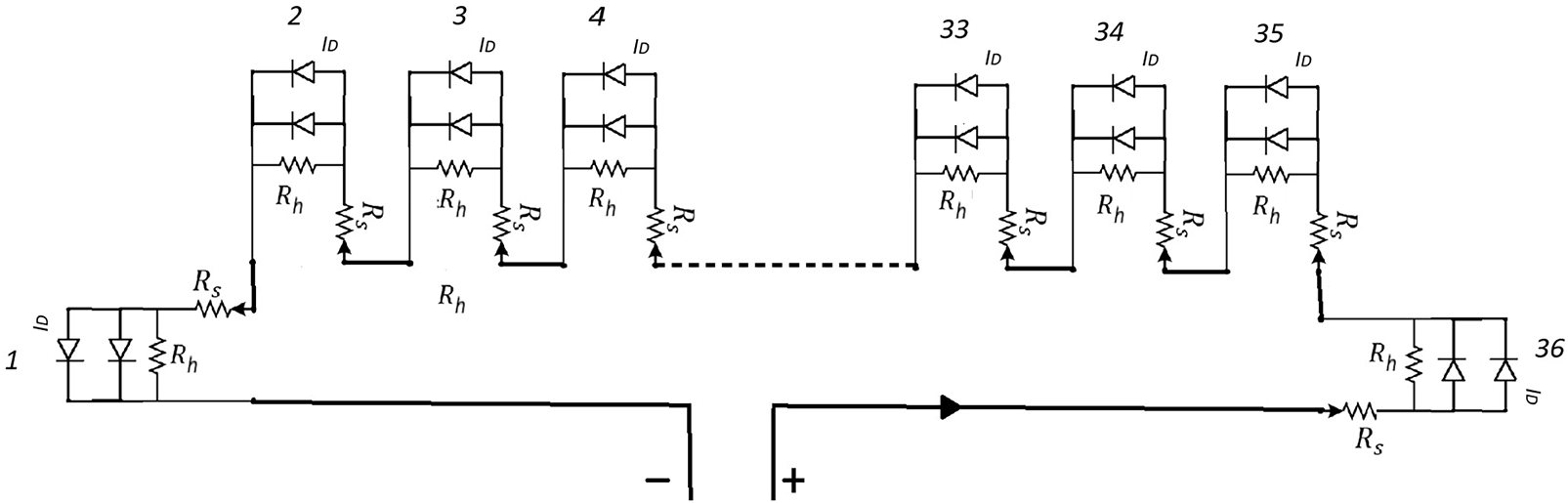
Figure 5: The equivalent circuit of a solar panel under study at dark conditions.
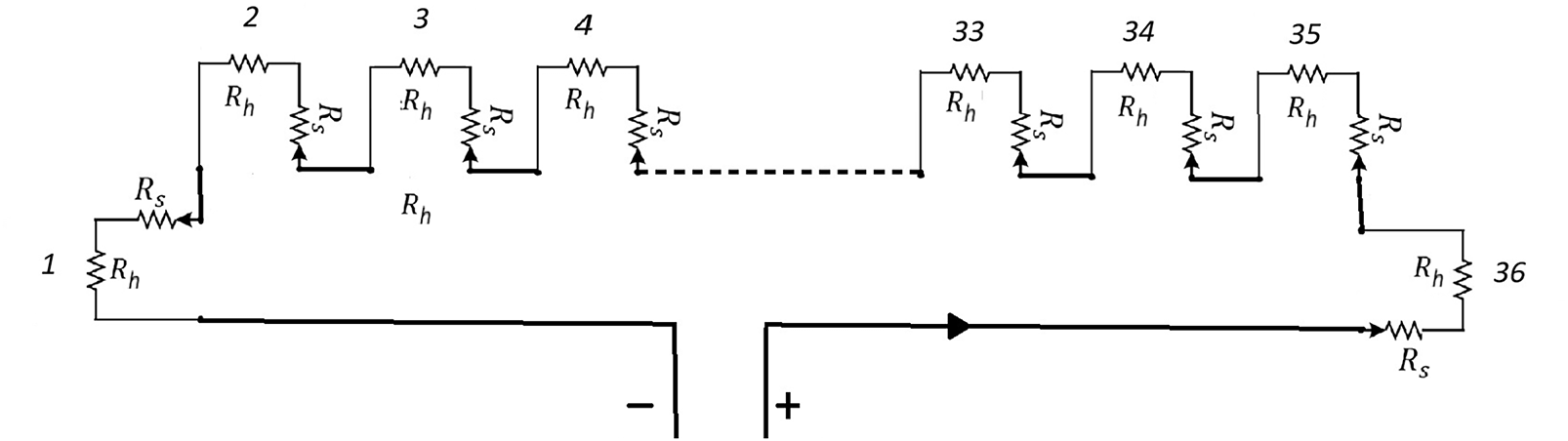
Figure 6: The equivalent circuit of a solar panel at lower I-V regions with dark conditions.
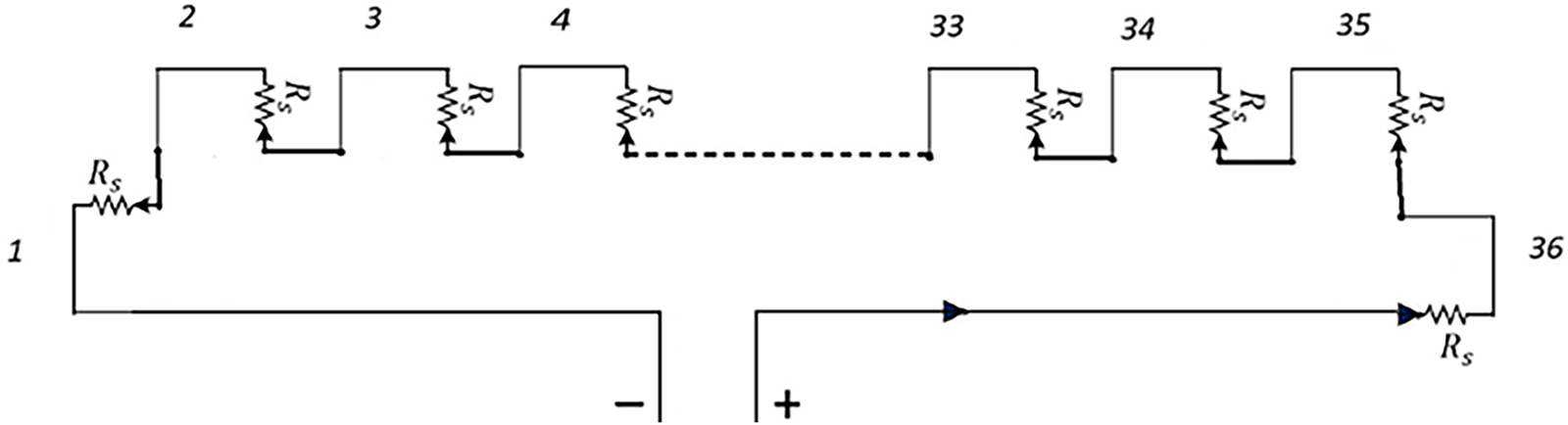
Figure 7: The equivalent circuit of a solar panel at higher I-V regions with dark conditions.
Accordingly, with the aid of the circuit diagrams of Figs. 5–7 and the captured measurements, the required static parameters are calculated using regression approaches for the developed curve of Fig. 4. Both the higher and the lower I-V regions of the curve were separated, and ranges of measurements have been selected that were deemed to most likely allow a successful ‘fit’ to the curves. For the higher part I-V characteristic, the curve can be fitted using the relation in (3) by neglecting the influence from the lower range.
After that, Eq. (4) is then used to calculate the lower part characteristics as follows:
Finally, a value for
MATLAB generalised linear model [16] is utilized in this research to extract the required static parameters per cell of the PV panel under study, and the final resultants are provided in Table 1
3 Evaluation of a PV Panel’s Dynamic Parameters at Dark Conditions
A PV cell can be modelled during dynamically variable input conditions as shown in Fig. 8, where the capacitance features taking place are the junction (Cj) and the diffusion capacitance (Cd) which are due to the carrier change in the space charge “junction” region and in the neutral regions, respectively. When the PV cell is reverse-biased, there are much fewer minority carriers in the neutral regions, so Cd diminishes, and Cj dominates. For forward-biased conditions, the contribution from the rearrangement of the minority carrier density is highly raised leading Cd to dominate Cj under such conditions. The variation of both constituents of the PV cell capacitances with an external voltage is illustrated in Fig. 9 [17].
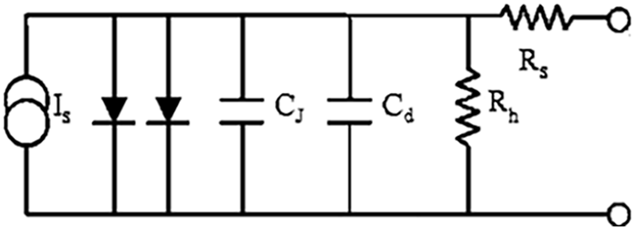
Figure 8: The circuit model of the PV cell at dynamic conditions.
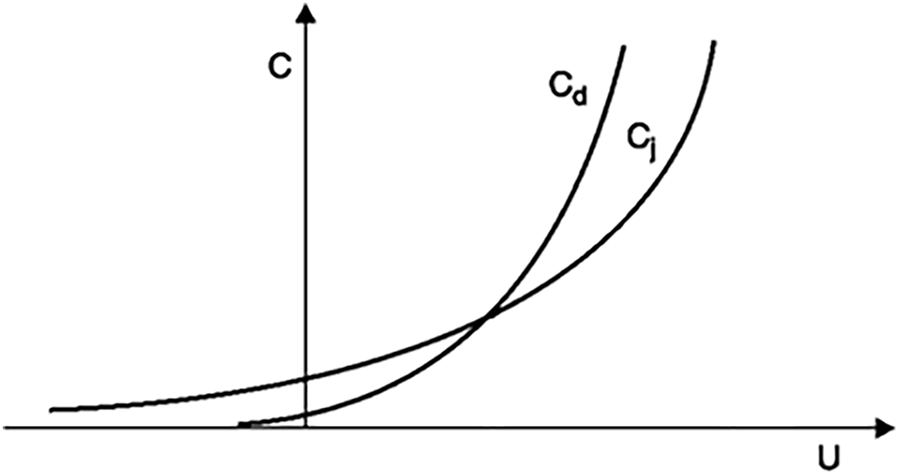
Figure 9: Typical variations of Cj and Cd with an external voltage.
3.1 Evaluation of Junction Capacitance Cj
Once the cell is in dark conditions and reverse-biased, photogeneration current and the diode currents will be mainly zeros. In addition, Cd becomes negligible as aforementioned, and the voltage drop in Rs as well. Accordingly, the circuit model of Fig. 8 would be simplified to the equivalent circuit in Fig. 10. In such conditions, the relationship between the voltage and the current of the PV cell can be written as given in (6).
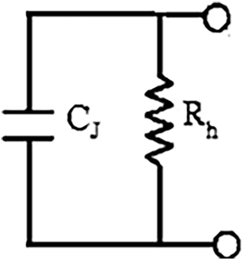
Figure 10: The simplified circuit model of the PV cell at reversed bias dark conditions.
This formula can be then utilised to estimate a junction capacitance value for every instantaneous value of the applied voltage at moderate frequencies in quasi-steady-state conditions [6].
A measuring approach has been developed in [6] to acquire the Cj of the PV cell which consists of a voltage ramp (with a rather slow, adjustable slope) and an operational amplifier. This approach is based in a design used by [18] for the measurement of the quasi-static capacitance of MOS structures. The negative feedback of the operational amplifier forces the reverse voltage in the cell to be equal to the ramp, and the output signal of the circuit to be proportional to the cell current.
Accordingly, this paper adopts a similar approach with modified circuits arrangements to be able to stimulate the whole 36 series connected cells PV panel under study, so that the corresponding Cj could be evaluated. Two cascaded LM3886 operational amplifier chips have been used in this paper, where the PV panel is connected as demonstrated in Fig. 11 and is reverse-biased. A photo of the developed circuit is shown in Fig. 12.

Figure 11: The circuit diagram in this research to evaluate the Cj of the PV panel under study.
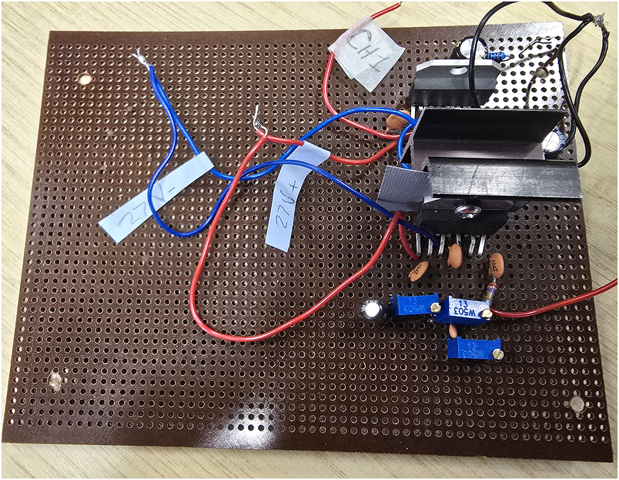
Figure 12: The developed circuit to evaluate the Cj.
Two Thurlby PL310 (30 V—1 A) power supplies were wired in series to provide +27 V and −27 V to provide supply voltages to the two LM3886 amplifiers used in the experimental setup. a 2 V ramp signal created by the AWG function of a Picoscope is applied to input pin 10 of the first LM3886 chip, so as to produce a 20 V signal at its output to pin 3 to feed into the PV panel through its negative terminal. An example of the input and output signals of the first LM3886 chip is illustrated in Fig. 13.
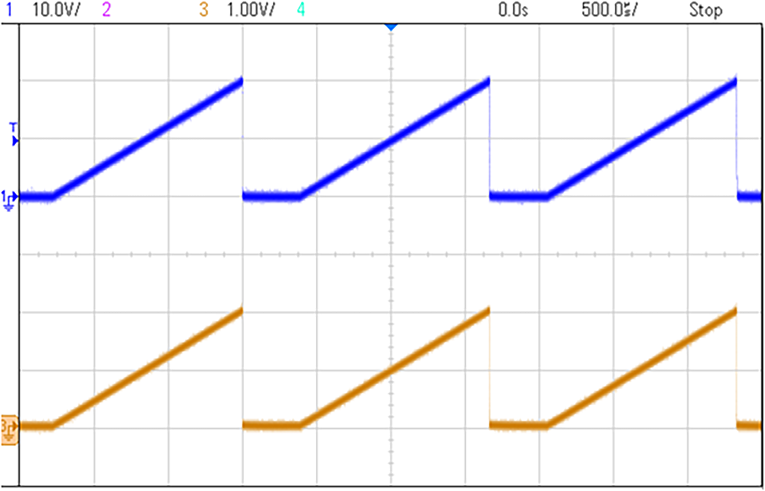
Figure 13: Input (orange) and output (blue) signals for the first LM3886 chip.
The overall equivalent circuit diagram for the PV panel under study at such experimental setup is provided in Fig. 14.
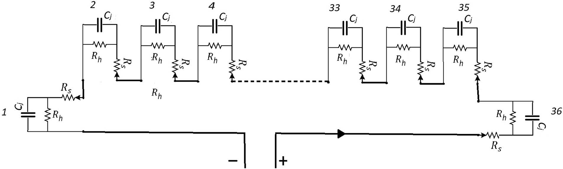
Figure 14: Equivalent circuit diagram of the PV panel at reversed biased connection.
The slope of the input ramp signal has to be selected not to be too slow, so the leakage current through the Rh would not be dominant and mask the capacitive current. Similarly, the fast ramps have to be avoided as it could lead to a saturation of the current channel. As a result, the input ramp signals are configured in this research to generate three different case studies:
1. 1 V @ 100 Hz
2. 1 V @ 500 Hz
3. 1 V @ 1 kHz
The PV panel voltage and current at these testing conditions are captured and an example of their waveforms at the case of the (1 V @ 1 kHz) is illustrated in Fig. 15.
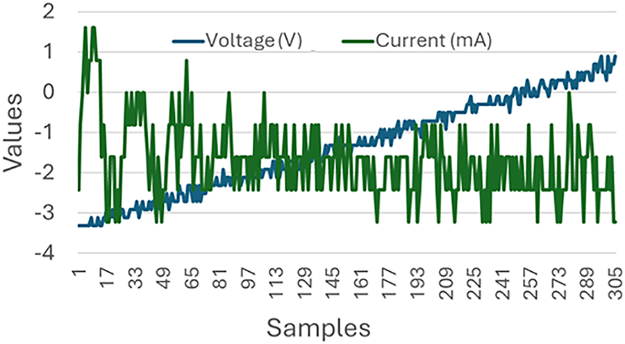
Figure 15: PV panel voltage and current at (1 V @ 1 kHz) ramp testing condition.
The measured data was then processed using the inbuilt Excel Data Analysis Toolbox, exponential smoothing was chosen with a damping factor of 0.90 as this was found to give the best results. The processed results of the waveforms shown in Fig. 15 are provided in Fig. 16.
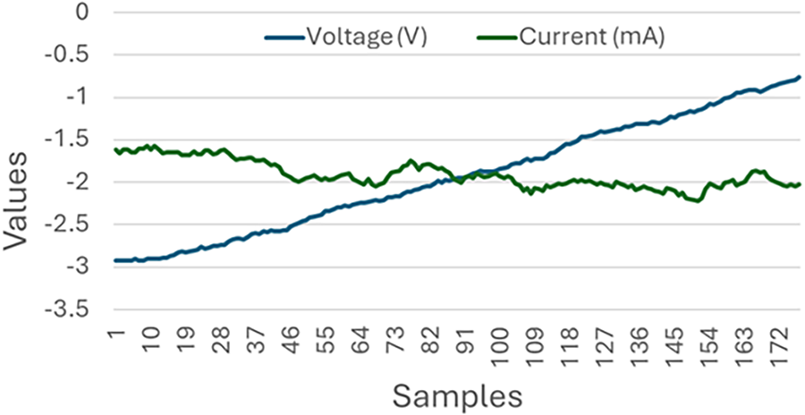
Figure 16: Postprocessed voltage and current data at (1 V @ 1 kHz) ramp testing condition.
Following from Eq. (6), the Cj per cell for the PV panel under study is evaluated as follows:
Accordingly, the Cj of the three testing scenarios is evaluated vs. the PV panel voltage and demonstrated as follows in Figs. 17–19.
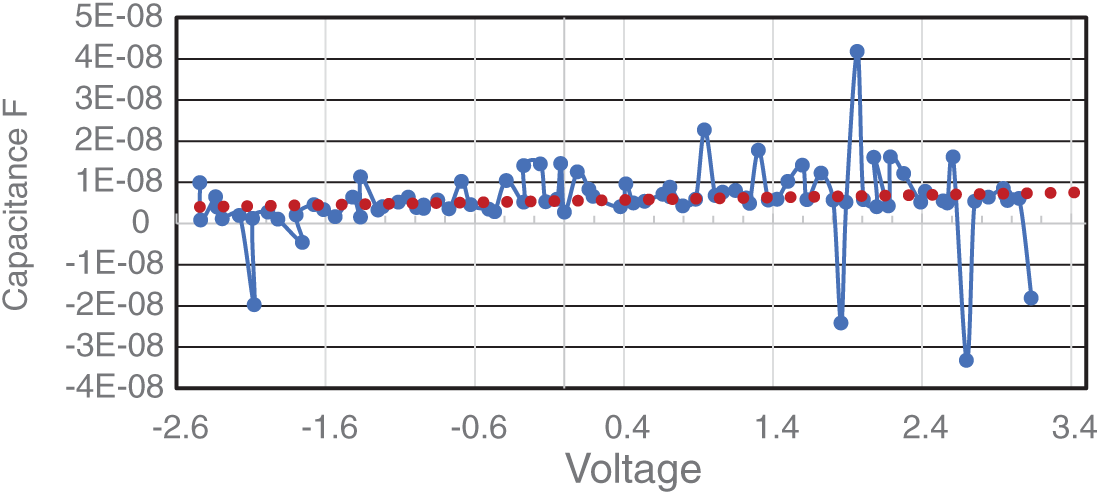
Figure 17: Evaluated Cj at 100 Hz testing condition vs. the PV panel voltage.
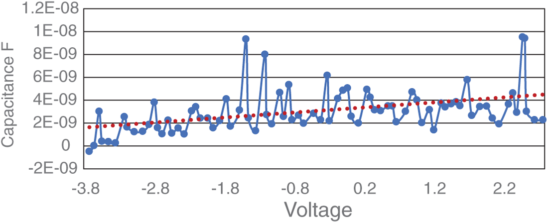
Figure 18: Evaluated Cj at 500 Hz testing condition vs. the PV panel voltage.
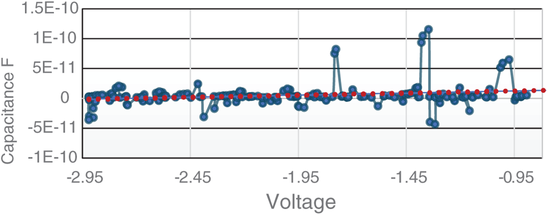
Figure 19: Evaluated Cj at 1 kHz testing condition vs. the PV panel voltage.
Figs. 17–19 show that the junction capacitance rises as the applied voltage rises, this is highlighted in each graph by an added trend line. Some anomalies can still be observed in these plots, where there appears to be outliers. Such rising profiles are also in alignment with the Cj pattern provided in Fig. 9.
The increasing junction capacitance of the solar panel relates to the increasing applied voltage due to the rise of mobile ions. The mobile ions increase with an increasing reverse dark current in a PN junction because of the way that the electric field and the dynamics of the carriers behave under these reverse bias conditions [5].
3.2 Evaluation of Diffusion Capacitance Cd
Diffusion capacitance
The diffusion capacitance is the key component of the solar circuits forward-biased dynamic character and is an outcome of the minority charge carrier storage in the neutral region and its diffusion ability.
where;
•
•
•
In the voltage range where
Usually, an OCVD signal exhibits three regions as can be seen in Fig. 20. The sharp drop in region (i) of Fig. 20 is attributed to the series resistance. The main impact of series resistance is to reduce the fill factor, but having extremely high values could also reduce the short-circuit current [24]. On the other hand, region (ii) is due to the diffusion and recombination of minority charge carriers into the quasi-neutral regions (QNR). This is being the region of interest for lifetime extraction.
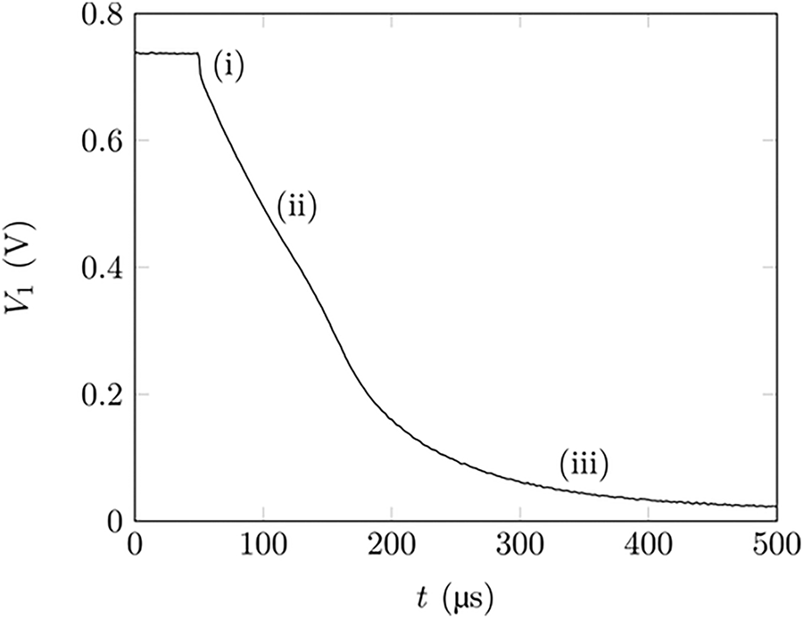
Figure 20: The decaying OCVD signal regions of interest [25].
Ideally, region (ii) presents a linear decay where the slope is inversely proportional to the effective lifetime
where;
• η is the p-n junction ideality factor,
•
•
• q is the elementary electric charge in coulombs,
•
OCVD experiments have been undertaken in this research to evaluate the Cd of the PV panel in a dark environment. A signal generator is used to control the switching of the square wave voltage across the panel using the MOSFET switching circuit and an oscilloscope to measure the input signal and the output voltage decay across the panel. The circuit diagram of the experimental setup is demonstrated in Fig. 21, while the schematic of the MOSFET switching circuit to produce the signal generator is illustrated in Fig. 22.
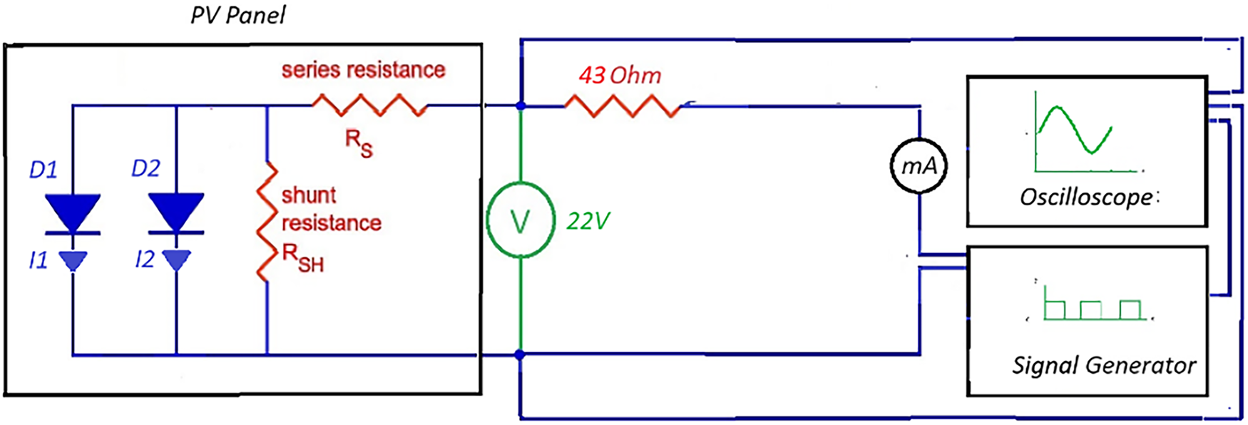
Figure 21: The circuit diagram used for the OCVD experiments in this research.
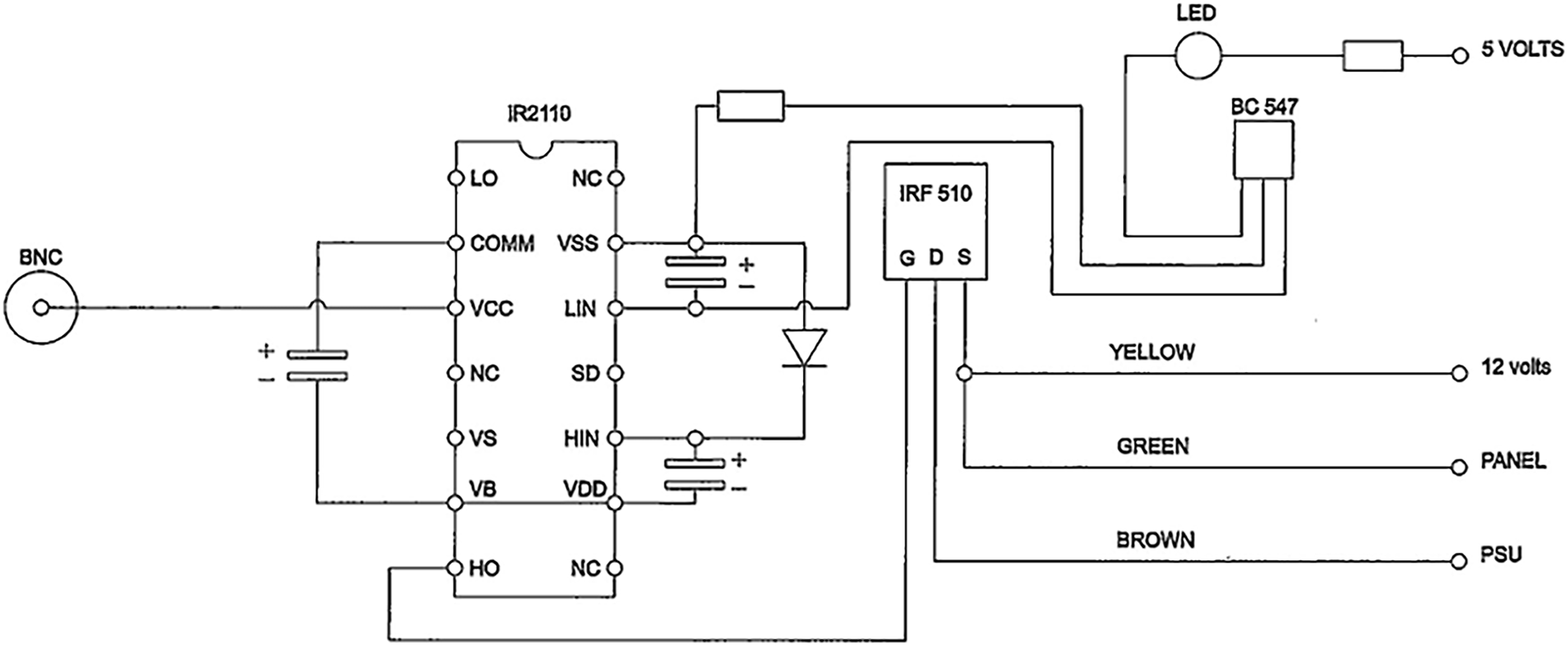
Figure 22: The schematic of the MOSFET switching circuit for the function generator.
The equipment used in this experimental setup is shown in Fig. 23, the MOSFET circuit is switching at 100 Hz in this setup and requires both a 12 and a 5 V supply to generate the required signal generator waveforms. Another power supply of 22 V is used to excite the PV panel under test. The MOSFET switching apparatus is used to switch the 22 V source across the panel and the oscilloscope was then used to both observe and record both the control signal and the resulting decay signals. Both waveforms are illustrated in Fig. 24.
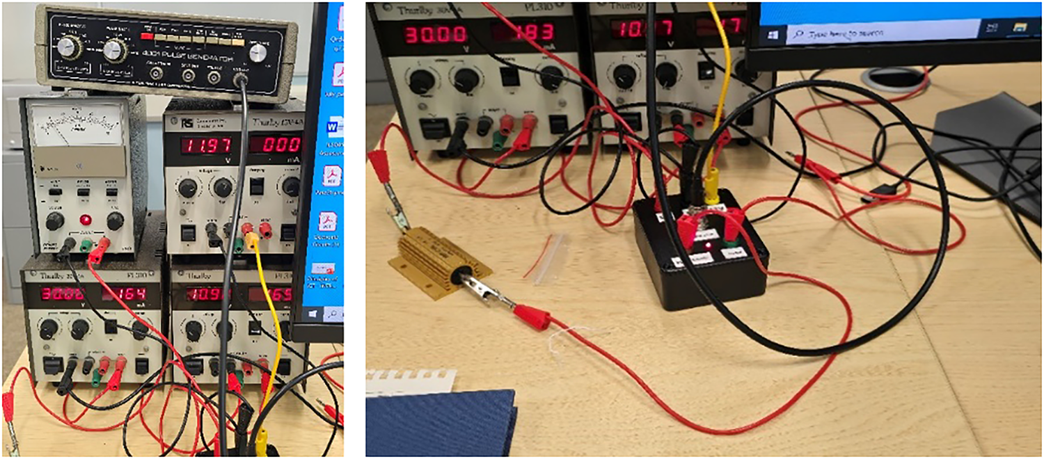
Figure 23: The apparatus used to switch the signal voltage across the panel.
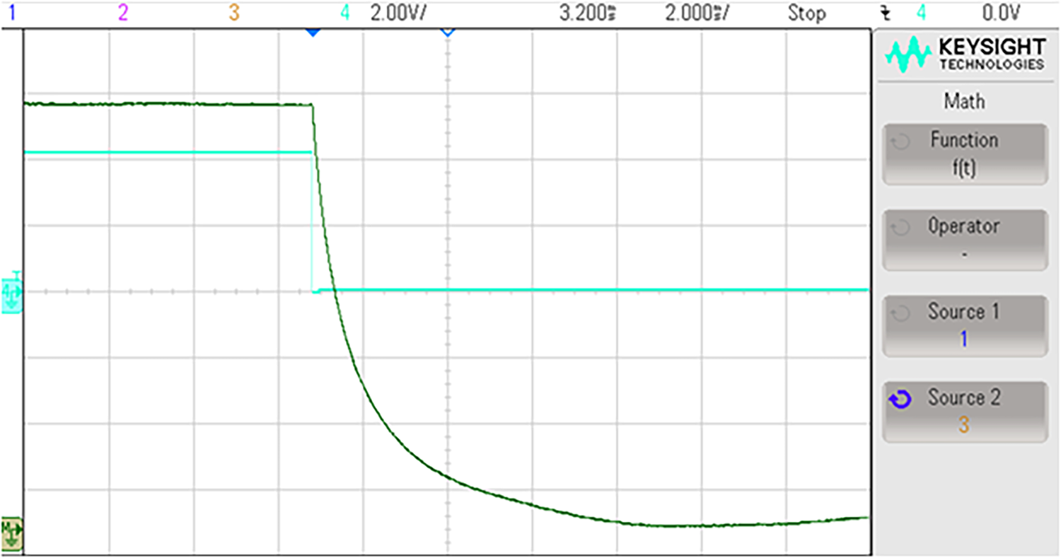
Figure 24: The control (light blue) and OCVD (green) signals of the experimental setup in this research.
The area of interest of the undertaken OCVD measurements is shown in Fig. 25 where region (ii) is highlighted by the red straight line. The captured data was imported into MS Excel to calculate the value(s) of
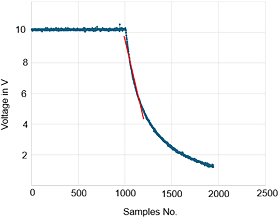
Figure 25: Highlighted region (ii) of the undertaken OCVD in this research.
The values for
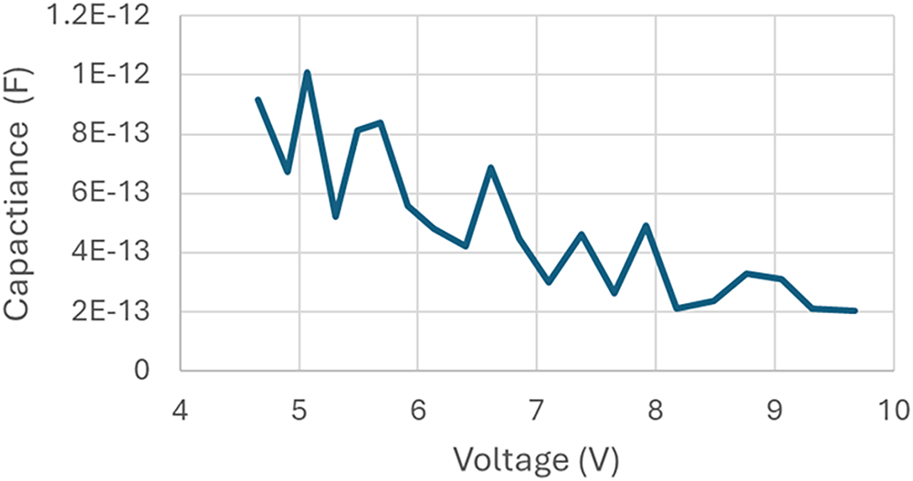
Figure 26: Evaluated Cd vs. the applied voltage.
The static and dynamic electrical parameters of a solar panel of 36 series-connected cells have been evaluated in this research by employing three different distinctive experimental setups in a dark environment. With respect to the static parameters, this paper has calculated the PV panel resultant diodes’ saturation currents, their diodes’ ideality factors, their series, and shunt resistances, where the results are summarised in Table 1. After that, the dynamic parameters are evaluated starting with Cj using the experimental setup of Fig. 11, where they are estimated at different switching conditions and demonstrated in Figs. 17–19. Eventually, Cd is evaluated using the unique OCVD setup of Fig. 21 and its value per cell is plotted vs. the applied voltage in Fig. 26, where its average is calculated to be 7.33 pF for the PV panel under study.
The evaluation of the static and dynamic electrical parameters of solar panels is crucial for accurate performance assessment, system design and optimisation, and ensuring long-term reliability and safety. Static parameters define the solar panel’s performance under stable and static conditions, which is essential for informed purchasing decisions on system sizing and component compatibility, as well as quality control and efficiency assessment. On the other hand, dynamic parameters describe how a solar panel behaves under real-world, constantly changing conditions to be used for their performance forecasting, optimisation of their maximum power point tracking algorithm, and also evaluating their degradation analysis.
The fundamental contributions of this research, to evaluate the parameters of a complete solar panel, become evident when comparing to the recent state-of-the-art literature, which explored a single solar cell. The interconnected nature of a PV module, which comprises of multiple cells, metallic interconnects, and other parasitic elements, all these factors create an extremely complex electrical environment when compared to a single solar cell. The distributed effects and the material defects of these electrical parameters were deemed to be outside of the primary scope of this investigation but clearly highlighted a need for careful examination and interpretation of the experimental data, as the panel’s response is surely influenced by these factors. Future works are aimed to be carried out in this area.
Acknowledgement: Not applicable.
Funding Statement: The authors received no specific funding for this study.
Author Contributions: Conceptualisation, Anthony Dyson, Marcel Ambroze; methodology, Anthony Dyson, Tamer Kamel; software validation, Anthony Dyson; formal analysis, Anthony Dyson, Tamer Kamel; investigation, Tamer Kamel, Marcel Ambroze; resources, Tamer Kamel, Marcel Ambroze; writing—original draft preparation, Anthony Dyson, Tamer Kamel; writing—review and editing, Tamer Kamel, Marcel Ambroze; visualization, Anthony Dyson, Tamer Kamel; supervision, Tamer Kamel, Marcel Ambroze. All authors reviewed and approved the final version of the manuscript.
Availability of Data and Materials: The data that supports the findings of this study are available from the corresponding author Tamer Kamel upon reasonable request.
Ethics Approval: Not applicable.
Conflicts of Interest: The authors declare no conflicts of interest.
References
1. Luque A, Hegedus S. Handbook of photovoltaic science and engineering. Hoboken, NJ, USA: John Wiley & Sons, Inc.; 2011. doi:10.1002/9780470974704. [Google Scholar] [CrossRef]
2. Aghaei M, Fairbrother A, Gok A, Ahmad S, Kazim S, Lobato K, et al. Review of degradation and failure phenomena in photovoltaic modules. Renew Sustain Energy Rev. 2022;159:112160. doi:10.1016/j.rser.2022.112160. [Google Scholar] [CrossRef]
3. McEvoy A, Castañer L, Markvart T. Solar cells: materials, manufacture and operation. Cambridge, MA, USA: Academic Press; 2012. doi:10.1016/C2011-0-07789-X. [Google Scholar] [CrossRef]
4. Recart F, Cuevas A. Application of junction capacitance measurements to the characterization of solar cells. IEEE Trans Electron Devices. 2006;53(3):442–8. doi:10.1109/ted.2006.870846. [Google Scholar] [CrossRef]
5. Tifidat K, Maouhoub N. An efficient method for predicting PV modules performance based on the two-diode model and adaptable to the single-diode model. Renew Energy. 2023;216(2):119102. doi:10.1016/j.renene.2023.119102. [Google Scholar] [CrossRef]
6. Virtuani A, Müllejans H, Dunlop ED. Comparison of indoor and outdoor performance measurements of recent commercially available solar modules. Prog Photovolt Res Appl. 2011;19(1):11–20. doi:10.1002/pip.977. [Google Scholar] [CrossRef]
7. Adak S, Cangi H. The quality problems at low irradiance in the grid-connected photovoltaic systems. Electr Eng. 2024;106(5):6185–97. doi:10.1007/s00202-024-02351-6. [Google Scholar] [CrossRef]
8. Adak S, Cangi H, Eid B, Yilmaz AS. Developed analytical expression for current harmonic distortion of the PV system’s inverter in relation to the solar irradiance and temperature. Electr Eng. 2021;103(1):697–704. doi:10.1007/s00202-020-01110-7. [Google Scholar] [CrossRef]
9. Aguilar J, Pavon W, Dehouche Z. Experimental characterization of a commercial photovoltaic thermal (PVT) hybrid panel under variable hydrodynamic and thermal conditions. Energies. 2025;18(13):3373. doi:10.3390/en18133373. [Google Scholar] [CrossRef]
10. Sredenšek K, Simonič E, Deželak K, Bizjak M, Lukač N, Seme S. Dynamic modeling and experimental validation of the photovoltaic/thermal system. Appl Sci. 2025;15(19):10505. doi:10.3390/app151910505. [Google Scholar] [CrossRef]
11. Wang S, Yu Y, Hu W. Static and dynamic solar photovoltaic models’ parameters estimation using hybrid Rao optimization algorithm. J Clean Prod. 2021;315:128080. doi:10.1016/j.jclepro.2021.128080. [Google Scholar] [CrossRef]
12. Abdel-Basset M, Mohamed R, Chakrabortty RK, Sallam K, Ryan MJ. An efficient teaching-learning-based optimization algorithm for parameters identification of photovoltaic models: analysis and validations. Energy Convers Manag. 2021;227(3):113614. doi:10.1016/j.enconman.2020.113614. [Google Scholar] [CrossRef]
13. Liang J, Ge S, Qu B, Yu K, Liu F, Yang H, et al. Classified perturbation mutation based particle swarm optimization algorithm for parameters extraction of photovoltaic models. Energy Convers Manag. 2020;203:112138. doi:10.1016/j.enconman.2019.112138. [Google Scholar] [CrossRef]
14. Weng X, Heidari AA, Liang G, Chen H, Ma X, Mafarja M, et al. Laplacian Nelder-Mead spherical evolution for parameter estimation of photovoltaic models. Energy Convers Manag. 2021;243(3):114223. doi:10.1016/j.enconman.2021.114223. [Google Scholar] [CrossRef]
15. Kaminski A, Marchand JJ, Fave A, Laugier A. New method of parameters extraction from dark I-V curve. In: Proceedings of the Conference Record of the Twenty Sixth IEEE Photovoltaic Specialists Conference—1997; 1997 Sep 29–Oct 3; Anaheim, CA, USA. p. 203–6. doi:10.1109/PVSC.1997.654064. [Google Scholar] [CrossRef]
16. The MathWorks, Inc. Generalized linear models [Internet]. 2023 [cited 2026 Jan 1]. Available from: https://uk.mathworks.com/help/stats/generalized-linear-regression.html. [Google Scholar]
17. Salach-Bielecki R, Pisarkiewicz T, Stapinski T, Wójcik P. Influence of junction parameters on the open circuit voltage decay in solar cells. Opto-Electron Rev. 2004;12(1):79–83. [Google Scholar]
18. Kuhn M. A quasi-static technique for MOS C-V and surface state measurements. Solid State Electron. 1970;13(6):873–85. doi:10.1016/0038-1101(70)90073-0. [Google Scholar] [CrossRef]
19. Ali Khan Niazi K, Yang Y, Kerekes T, Sera D. Reconfigurable distributed power electronics technique for solar PV systems. Electronics. 2021;10(9):1121. doi:10.3390/electronics10091121. [Google Scholar] [CrossRef]
20. Sze SM, Ng KK. Physics of semiconductor devices. 3rd ed. Hoboken, NJ, USA: John Wiley & Sons, Inc.; 2007. [Google Scholar]
21. Green MA. Minority carrier lifetimes using compensated differental open circuit voltage decay. Solid State Electron. 1983;26(11):1117–22. doi:10.1016/0038-1101(83)90011-4. [Google Scholar] [CrossRef]
22. Pravettoni M, Poh D, Prakash Singh J, Wei Ho J, Nakayashiki K. The effect of capacitance on high-efficiency photovoltaic modules: a review of testing methods and related uncertainties. J Phys D Appl Phys. 2021;54(19):193001. doi:10.1088/1361-6463/abe574. [Google Scholar] [CrossRef]
23. Lederhandler SR, Giacoletto LJ. Measurement of minority carrier lifetime and surface effects in junction devices. Proc IRE. 1955;43(4):477–83. doi:10.1109/JRPROC.1955.277857. [Google Scholar] [CrossRef]
24. PV education module circuit design [Internet]. [cited 2026 Jan 1]. Available from: https://www.pveducation.org/pvcdrom/modules-and-arrays/module-circuit-design. [Google Scholar]
25. Ruch B, Jech M, Pobegen G, Grasser T. Applicability of Shockley–read–hall theory for interface states. IEEE Trans Electron Devices. 2021;68(4):2092–7. doi:10.1109/ted.2021.3049760. [Google Scholar] [CrossRef]
26. Monokroussos C, Gottschalg R, Tiwari AN, Friesen G, Chianese D, Mau S. The effects of solar cell capacitance on calibration accuracy when using a flash simulator. In: Proceedings of the 2006 IEEE 4th World Conference on Photovoltaic Energy Conference; 2006 May 7–12; Waikoloa, HI, USA. p. 2231–4. doi:10.1109/WCPEC.2006.279953. [Google Scholar] [CrossRef]
Vedel CD, Gunst T, Smidstrup S, Georgiev VP. Shockley-Read-Hall recombination and trap levels in In0.53Ga0.47As point defects from first principles. Phys Rev B. 2023;108(9):094113. doi:10.1103/physrevb.108.094113. [Google Scholar] [CrossRef]
Cite This Article
 Copyright © 2026 The Author(s). Published by Tech Science Press.
This work is licensed under a Creative Commons Attribution 4.0 International License , which permits unrestricted use, distribution, and reproduction in any medium, provided the original work is properly cited.
 Downloads
 Citation Tools