
 Submit a Paper
 Propose a Special lssue
 Open Access
ARTICLE
Genetic Algorithm Based 7-Level Step-Up Inverter with Reduced Harmonics and Switching Devices
1 Department of EEE, Dr. Mahalingam College of Engineering and Technology, Pollachi, Tamilnadu, India
2 Department of EEE, PSNA College of Engineering and Technology, Dindigul, Tamilnadu, India
* Corresponding Author: T. Anand Kumar. Email:
Intelligent Automation & Soft Computing 2023, 35(3), 3081-3097. https://doi.org/10.32604/iasc.2023.028769
Received 17 February 2022; Accepted 26 April 2022; Issue published 17 August 2022
 View Full Text
 Download PDF
Abstract
This paper presents a unique voltage-raising topology for a single-phase seven-level inverter with triple output voltage gain using single input source and two switched capacitors. The output voltage has been boosted up to three times the value of input voltage by configuring the switched capacitors in series and parallel combinations which eliminates the use of additional step-up converters and transformers. The selective harmonic elimination (SHE) approach is used to remove the lower-order harmonics. The optimal switching angles for SHE is determined using the genetic algorithm. These switching angles are combined with a level-shifted pulse width modulation (PWM) technique for pulse generation, resulting in reduced total harmonic distortion (THD). A detailed comparison has been made against other relevant seven-level inverter topologies in terms of the number of switches, drivers, diodes, capacitors, and boosting facilities to emphasize the benefits of the proposed model. The proposed topology is simulated using MATLAB/SIMULINK and an experimental prototype has been developed to validate the results. The Digital Signal Processing (DSP) TMS320F2812 board is used to generate the switching pulses for the proposed technique and the experimental results concur with the simulated model outputs.Keywords
Multilevel Inverter (MLI) is a popular choice across industry and academia because they are well suited for medium and high-power energy conversion. MLIs produce better staircase waveform compared to two-level inverters and also possess additional benefits namely; reduction in switching losses, voltage stress (dv/dt), total harmonic distortion, and filter size which leads to wide utilization in industrial applications [1]. Most familiar conventional MLI topologies are (i) Flying Capacitor MLI (FCMLI) [2], (ii) Neutral Point Diode Clamped MLI (NPDCMLI) [3] and (iii) Cascaded H-Bridge MLI (CHBMLI) [4]. As far as NPDCMLI is concerned more numbers of switching devices are required as well as the capacitor voltage sharing is unequal, resulting in increased voltage stress across the switches [5]. In the case of FCMLI, more complex control is required because it contains more flying capacitors, which increases both the system’s size and overall cost [6]. In the case of CHBMLI, more than one h-bridge and isolated DC sources are required to increase the output voltage levels [7–9]. CHBMLI is further classified as symmetric MLI and asymmetric MLI. Asymmetric MLI generates more output voltage levels than symmetric MLI [10,11]. Voltage boosting is essential in MLI when used in solar and electric vehicle applications. CHBMLI utilizes transformers to boost the output voltage gain, resulting in an oversized and bulkier system [12,13]. Transformer-less circuit designs were proposed as a solution to this problem by [14,15]. Although the use of a front-end DC-DC converter and energy buffer circuit eliminates the need for a transformer, the control complexity appears to be high in [14,15].
Packed U-Cell (PUC) is another evolving switched-capacitor (SC) based single input MLI topology, which is discussed in [16,17]. Despite the ability to generate the required number of output levels, the system lags in the output voltage boosting facility [16,17]. Similar to PUC, the topology with reduced device is proposed in [18]. It requires only seven switches and two diodes to produces the seven levels. Although it just requires a few devices, it falls short in terms of voltage boosting and requires three capacitors. In comparison to [18], the paper [19] exhibits improvements as it only requires eight switches and two capacitors to generate seven levels with 1.5 times the boosting factor. Using the level shifted PWM technique, the seven levels were generated with only eight switches and two capacitors [20].
Several seven-level (7L) topologies based on the three times boosting gain are presented in the following literature. In the proposed model [21], 16 switches with two capacitors are used to produce seven levels across the load. Similarly, with only 12 switches, the topology could generate seven levels of output voltage [22,23]. In comparison to [22,23], the structure only requires 11 switches to reach the required seven levels of output voltage [24]. A 7L inverter with sixteen switches and two capacitors are discussed in this study [25]. Despite the fact that this topology is capable of producing seven levels of output voltage, it necessitates the inclusion of additional switching devices. As a result, the system’s overall cost shoots up. In [26], a multipurpose inverter topology has been proposed for standalone applications. Despite the fact that it can attain seven levels of output voltage, this design still necessitates 13 switches and three battery sources. The following are the benefits of the proposed inverter as stated in this paper:
i) A single isolated DC source is sufficient for the proposed 7L inverter.
ii) Only 11 switches and two capacitors are required.
iii) Output voltage gain is boosted to thrice the value of input voltage (1:3) without using any additional inductor or transformer.
iv) Sensorless control for voltage balancing across the capacitors is achieved.
v) To minimize power loss across the switches, high-power switches are designed to operate at the fundamental frequency.
The functions of the suggested inverter are discussed in the following sections.
In Section 2, an overview of the topology and its operating modes are described.
In Section 3, the switching strategy and harmonic reduction techniques are discussed.
In Section 4, the power loss calculation has been discussed.
In Section 5, a detailed comparison has been made with various relevant topologies.
In Section 6, simulation and hardware results are described and concluded in Section 7.
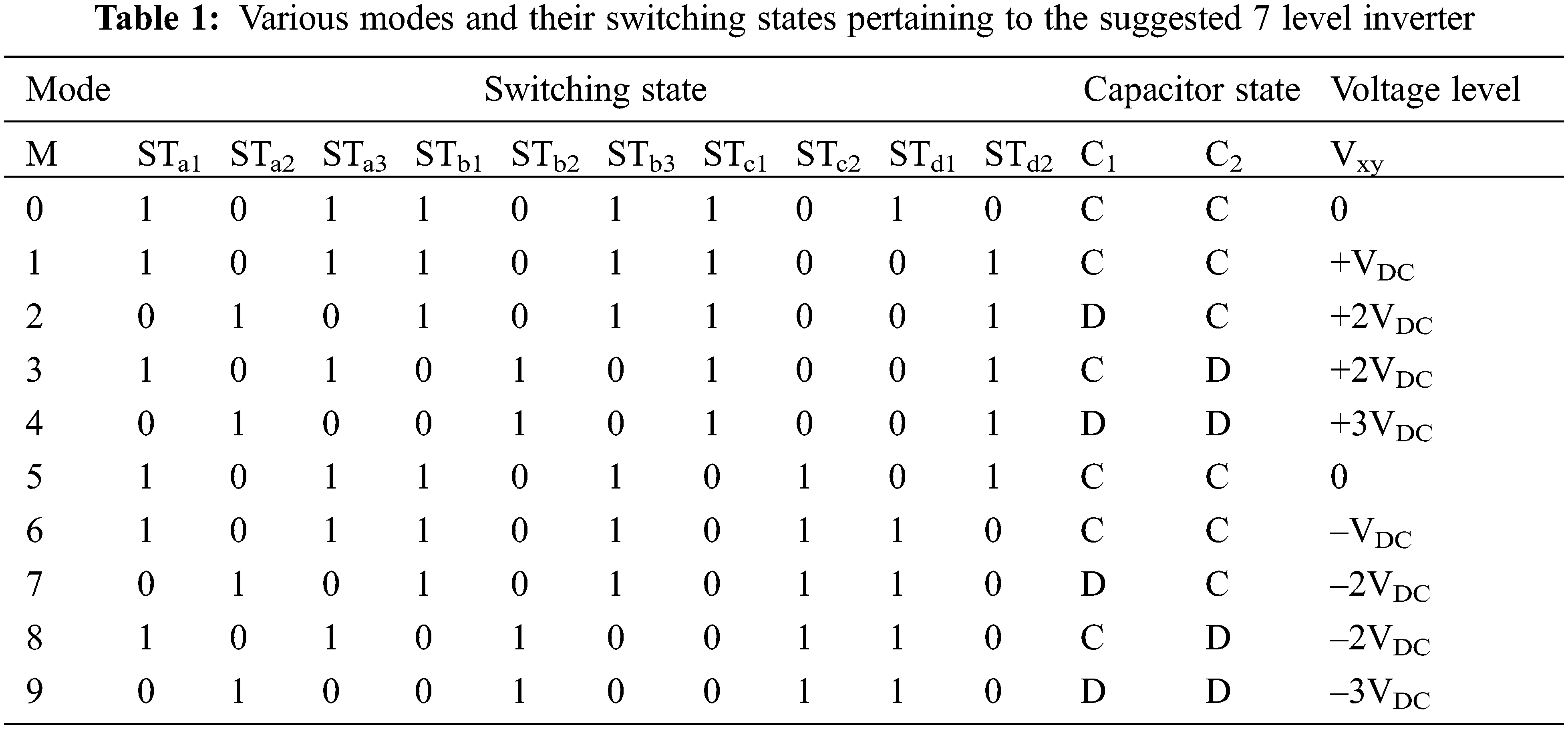
The proposed single-phase 7L switched-capacitor based topology has been represented in Fig. 1. The proposed circuit consists of nine unidirectional and one bidirectional power semiconductor switch (a total of 11 switches). The various operating states of the suggested topology have been illustrated through the equivalent circuits as shown in Fig. 2. It is essential to specify that the switches STa1 and STa3 are complementary with the switch STa2 during the entire operating mode. Similarly, STb1 and STb3 are working inverse to the switch STb2. These complimentary switching states ensure that the switched capacitors are charged without any interruption. This charged energy is later used to elevate the load voltage gain up to thrice that of the input value. Switching pairs of (STc1; STc2) and (STd1; STd2) cannot be activated simultaneously, as this results in a short of input DC voltage source (VDC). The seven different load voltage levels of 0, ±VDC, ±2VDC, and, ±3VDC are achieved through the various switching states as shown in Tab. 1. It is a significant constraint that during the peak level of ±3VDC, the negative voltage of the input source is blocked at node t and bypassed to node r using bidirectional switch STb3.
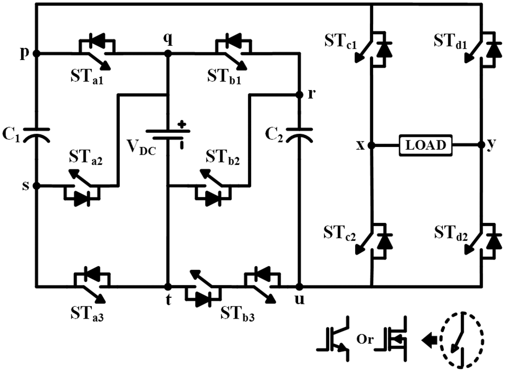
Figure 1: Proposed topology of 7 L inverter
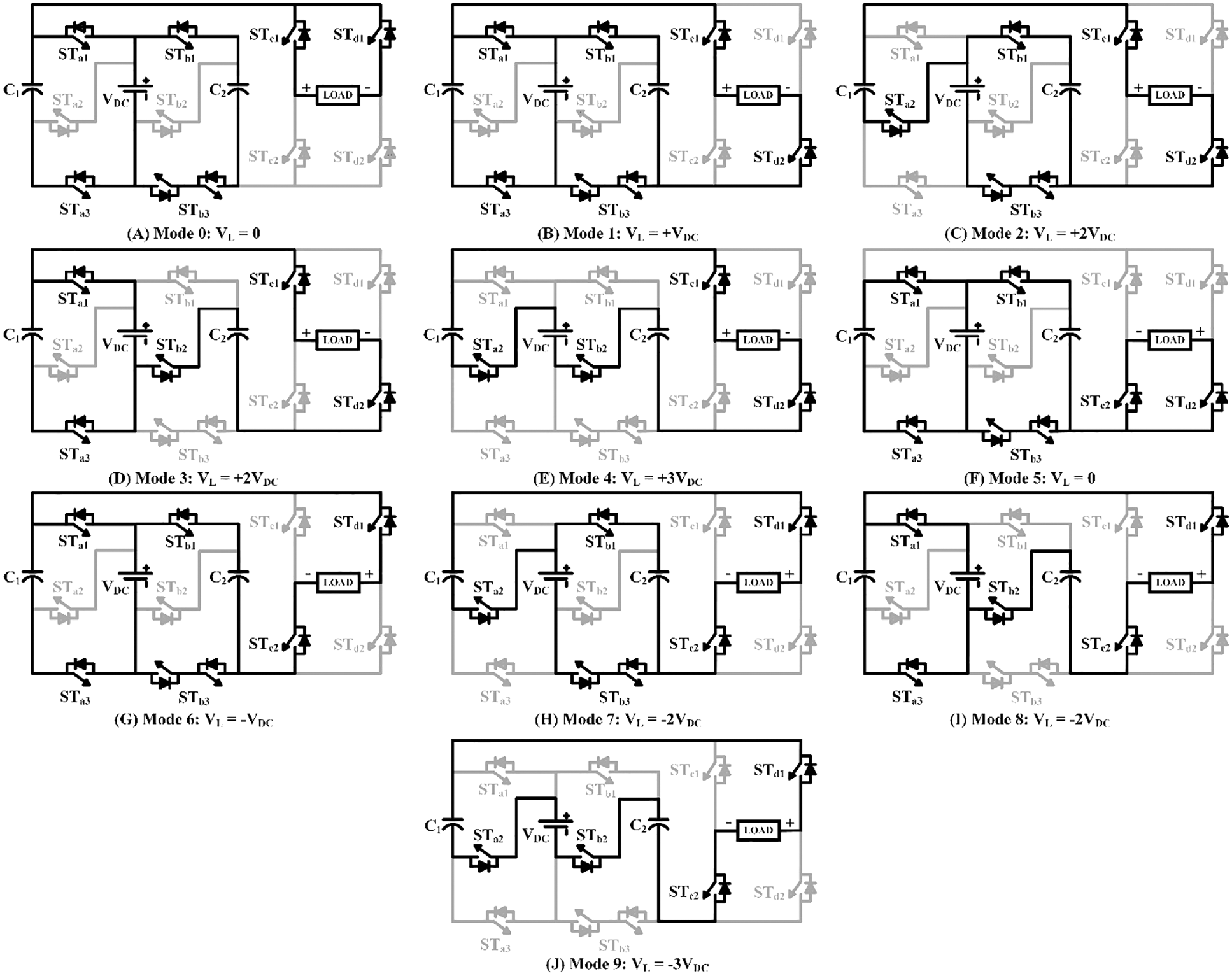
Figure 2: Various operating modes of the suggested 7 L switched-capacitor inverter
2.1 Modeling of the Proposed Circuit
The various modes of operation can be evaluated through the derived switching model as follows. Let the dynamic function of the switches during (k = 1, 2) are STak; STbk; STck and STdk respectively. The dynamic functions of the various modes can be obtained through the following equations,
The load voltage can be calculated as follows:
where the nodes are labeled as p, q, r, s, t, u, x, and y in Fig. 1 are expressed based on the switching function values.
Substituting Eq. (6) in Eq. (5) returns,
When k = 1 and k = 2, the output load voltage (Vout) is proportional to the positive and negative cycles, respectively in Eq. (7).
The various switching states and operating modes of the 7L inverter are depicted in Tab. 1 and in Fig. 2. The charging (C) and discharging (D) states of the capacitors are represented in Tab. 1.
Mode 0 (Vout = 0): In this zeroth level, as shown in Fig. 2A, the switches STa1, STa3, STb1, STb3, STc1 and STd1 are turned on and delivers zero voltage across the load. During this mode, the two capacitors C1 and C2 are in charging states. With k = 1, the Eq. (7) can be written as,
Mode 1 (Vout = +VDC): In this first level, as shown in Fig. 2B, the output voltage of (+VDC) has been generated across the load by triggering the switches STa1, STa3, STb1, STb3, STc1 and STd2. In this mode, the input DC source charges the capacitors voltage to VDC.
Mode 2 (Vout = +2VDC): The source voltage VDC and the discharging capacitor voltage VC1 were combined to create the second level, as shown in Fig. 2C. Furthermore, by actuating the switches STa2, STb1, STb3, STc1 and STd2, the capacitor C2 has been kept in a charging mode.
Mode 3 (Vout = +2VDC): This state has been redundant to Mode 2 as it generates (+ 2VDC) voltage level by triggering the switches STa1, STa3, STb2, STc1 and STd2. Capacitor C2 discharges with VDC and C1 remains charged, as seen in Fig. 2D.
Mode 4 (Vout = +3VDC): In the third level, maximum boosted voltage level of (+3VDC) is obtained by connecting all the capacitors in series with the input source. In this mode, only four switches (STa2, STb2, STc1 and STd2) are engaged, as shown in Fig. 2E.
The switching states in mode 5 are similar to mode 0, with the exception that the STc2 and STd1 switches are triggered instead of the STc1 and STd2 switches. The switching devices in modes 6, 7, 8 and 9 are similar to those in modes 1, 2, 3 and 4 except that instead of STc1 and STd2, the switches STc2 and STd1 are triggered.
The PWM strategies are employed to enhance the load voltage waveform in terms of distortion factor, lower-order harmonics, and total harmonic distortion (THD). PWM techniques are also categorized into three types based on their switching frequency: High, low, and hybrid switching frequency techniques (combination of low and high-frequency switching techniques). Some forms of high-switching frequency modulation techniques include the space vector PWM technique, carrier-based pulse width modulation technique as well as reference-based PWM technique. Low-frequency modulation technique includes fundamental frequency modulation, selective harmonic elimination PWM (SHEPWM) technique, and active harmonic elimination technique. CBPWM is classified into two types, level-shifted-carrier based PWM (LS-CBPWM) and phase-shifted-carrier based PWM (PS-CBPWM).
As illustrated in Fig. 3, the suggested inverter uses a PWM technique that combines the benefits of LS-CBPWM and SHEPWM to reduce harmonic content. In Fig. 3, the LS-CBPWM technique is demonstrated by comparing a reference sinusoidal waveform (Vref) with six equal-magnitude level-shifted carrier signals (Vcr). The carrier signal has a higher switching frequency to eliminate the lower order harmonics. Despite the fact that the LS-CBPWM can reduce THD, the harmonic profile is dominated by 3rd and 5th order harmonics. The Selective Harmonic Elimination technique is used to substantially eliminate the 3rd and 5th order harmonics in the output voltage. The GA optimization algorithm can be used to solve the SHEPWM’s nonlinear transcendental equations in order to generate the optimal switching angle [26]. The suggested seven level inverter’s switching angles of (α1, α2, α3) are generated by solving Eq. (18) with the constraint that αN must be less than
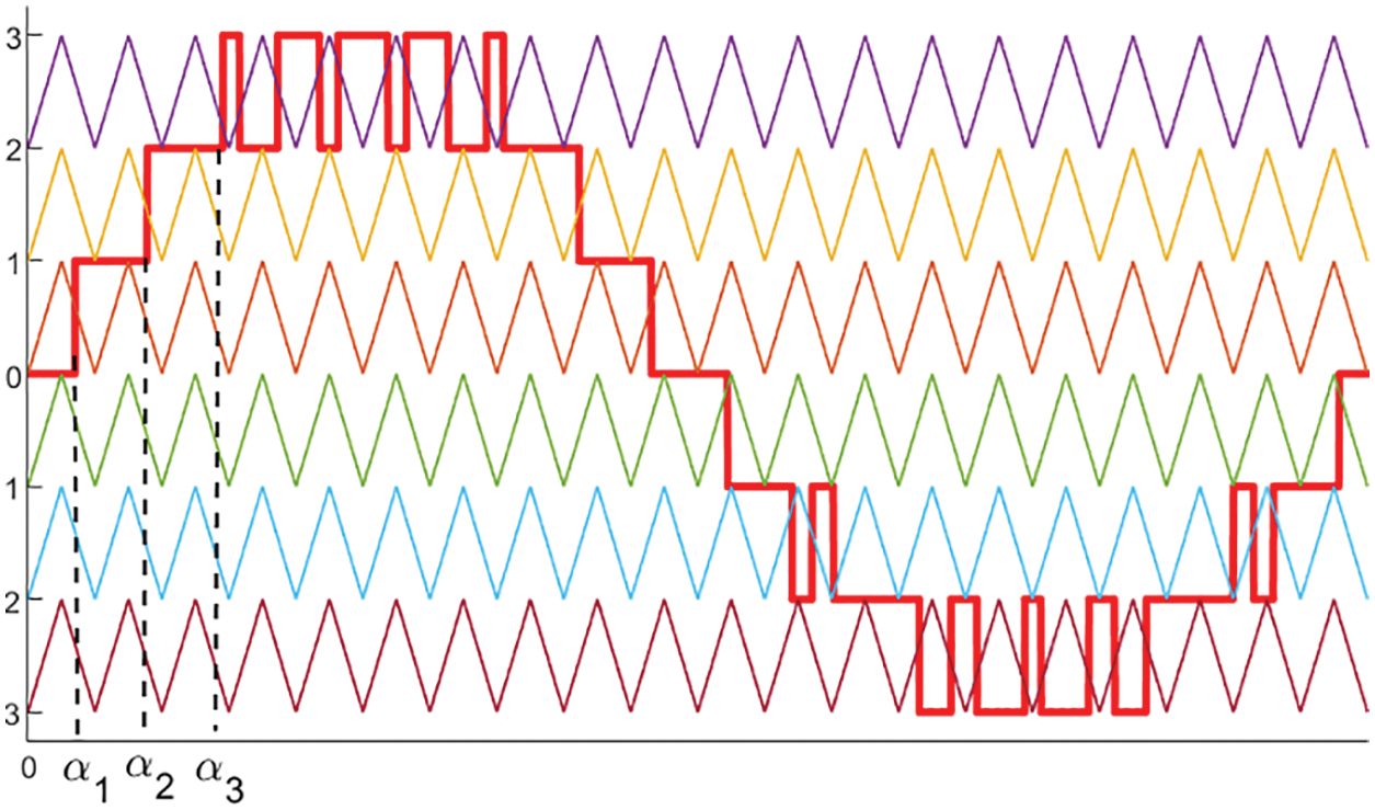
Figure 3: Pulse generation strategy for the proposed 7 L inverter
The multilevel output voltage waveform can be represented mathematically in a Fourier series, as given by,
The peak voltage of each nth harmonic component is provided by,
Eq. (14) can be used to compute the fundamental (V1) peak voltage as well as the 3rd and 5th order values.
Considering N switched sources, SHEPWM can minimize harmonics up to 2N-1. The inverter’s modulation index can be calculated by,
The modulation index with respect to number of levels can be derived as,
where 0 < α1 < α2 < ∙ ∙ ∙ < αN <
GA’s main purpose is to reduce the harmonic value to the smallest possible value, and the firing angles are also chosen by a genetic algorithm. The fitness function is represented as,
where V1* is the required peak of the fundamental component and it can be determined by the modulation index. The switching angles for various modulation index values are shown in Fig. 4a. Furthermore, the optimum switching angle is reached when the modulation index value is 0.8. The 3rd and 5th order harmonic percentages for various modulation index values are shown in Fig. 4b. Among the available modulation indexes, Fig. 4b displays the region with the least THD. As illustrated in Fig. 5, the capacitor voltage is stabilized by employing the voltage balancing algorithm technique between the C1 and C2 capacitors. The two C1 and C2 switched capacitors are charged to the DC source voltage level. Tab. 1 exhibits the charging and discharging of the proposed inverter. Furthermore, C1 and C2 capacitors are kept at charging mode during the 0 and ±VDC voltage levels and discharged during the ±3VDC voltage level. Furthermore, the C1 and C2 capacitors are charged during the 0 and ±VDC voltage levels, and discharged during the ±2VDC and ±3VDC voltage levels.
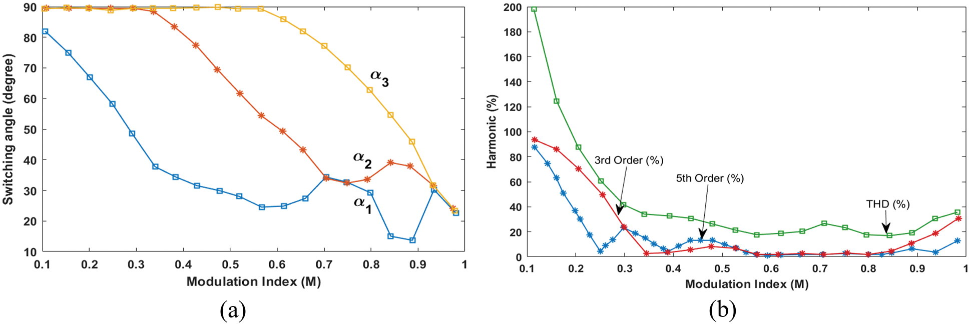
Figure 4: GA optimization results in terms of modulation index vs. (a) switching angle selection and (b) harmonic values
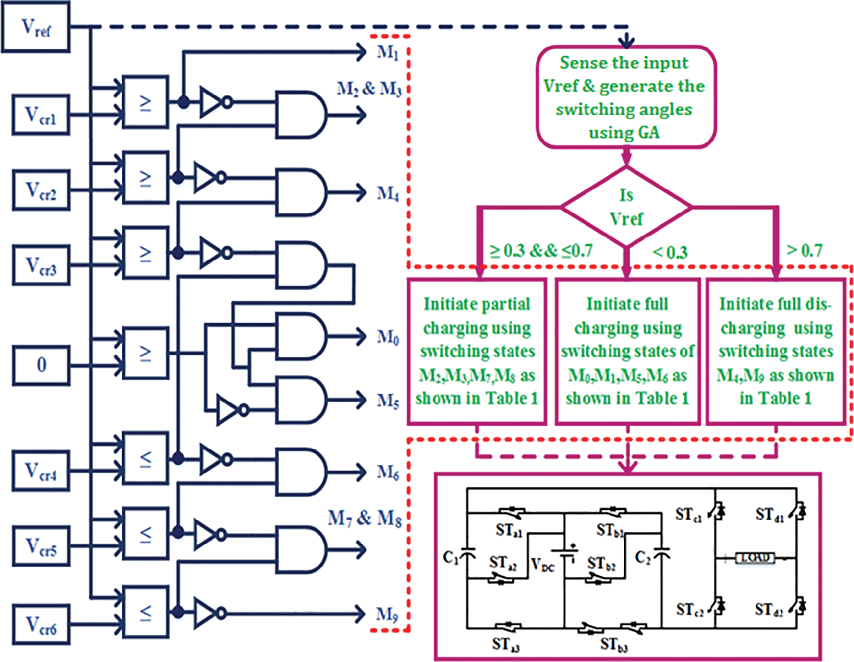
Figure 5: Self-balancing capacitor voltage algorithm with Genetic Algorithm
The conduction loss (Pcl) appears during the on-state of the power semiconductor switches, and mainly due to its internal resistance Rin. The (Pcl) can be calculated by
where Iout is the magnitude of the output current flows through the jth power switch.
The switching loss is caused by the overlap of current and voltage across the switches during the transition of switching states, i.e., from ON to OFF state, it is called as turn-on power loss (Pswl, ON) and from OFF to ON state called as a turn-off power loss (Pswl, OFF). In addition, these states have significant values in voltage and current magnitude, leading to switching power loss (Pswl).
The switching power loss can be calculated using Eqs. (20) and (21)
In the Eq. (22) fsj, VBlj, ton and toff is the switching frequency, blocking voltage and on-time and off-time of the of jth switch respectively.
Due to the capacitor equivalent series resistance (rESR) a voltage drop (Vcd) appears occurs across the capacitor. The ripple loss can be derived for any value of capacitance (Cp) is as follows
Eventually, using Eqs. (19), (22) and (23), the total power loss (Ploss) and efficiency (
where, Pin and Pout are the input and output powers of the inverter.
The advantages of the proposed system are demonstrated by contrasting it with other known conventional and related topologies. Tab. 2 shows a detailed comparison of the proposed model to other configurations in terms of total number of switches (Nsw), drivers (Ndriver), diodes (Ndiode), capacitors (Ncap), DC source (NDCS), switching devices (Ndevice), output voltage levels (NLevel), voltage stress (Vstress), gain ratio (G) and boosting facility. The comparison in Tab. 2 reveals that traditional topologies use more switching devices and have significant lag in the boosting facility. Topologies with triple times voltage boosting factors are described in this literature [14] and [21–25]. Even though, these topologies are identical in the number of output levels and gain they lag mostly in device count. The topology in [14] requires 13 switches, 4 diodes, and a total of 30 semiconductor devices. In comparison to the proposed model, the topology necessitates the use of more switches and diodes. The topology in [21] demands 16 switches and 14 gate driver circuits, a higher device count that results in higher power loss and cost. In [22,23], voltage stress across the switches is reduced to 2Vdc and requires only 12 switches. However, compared to the proposed model the total device count is higher. In [24], only 11 switches are required to generate 7 levels across the load, but three numbers of capacitors are required, resulting in control complexity. Topology [25] necessitates 5 additional switches than the proposed topology, resulting in increased cost and size. The device comparison in Fig. 6a illustrates that the proposed model only requires 11 switches and 10 gate driver circuits to generate the required 7L, which is significantly less than other topologies. Furthermore, the proposed model only requires two capacitors, resulting in a significant reduction in total cost and inverter size, as shown in Fig. 6b.
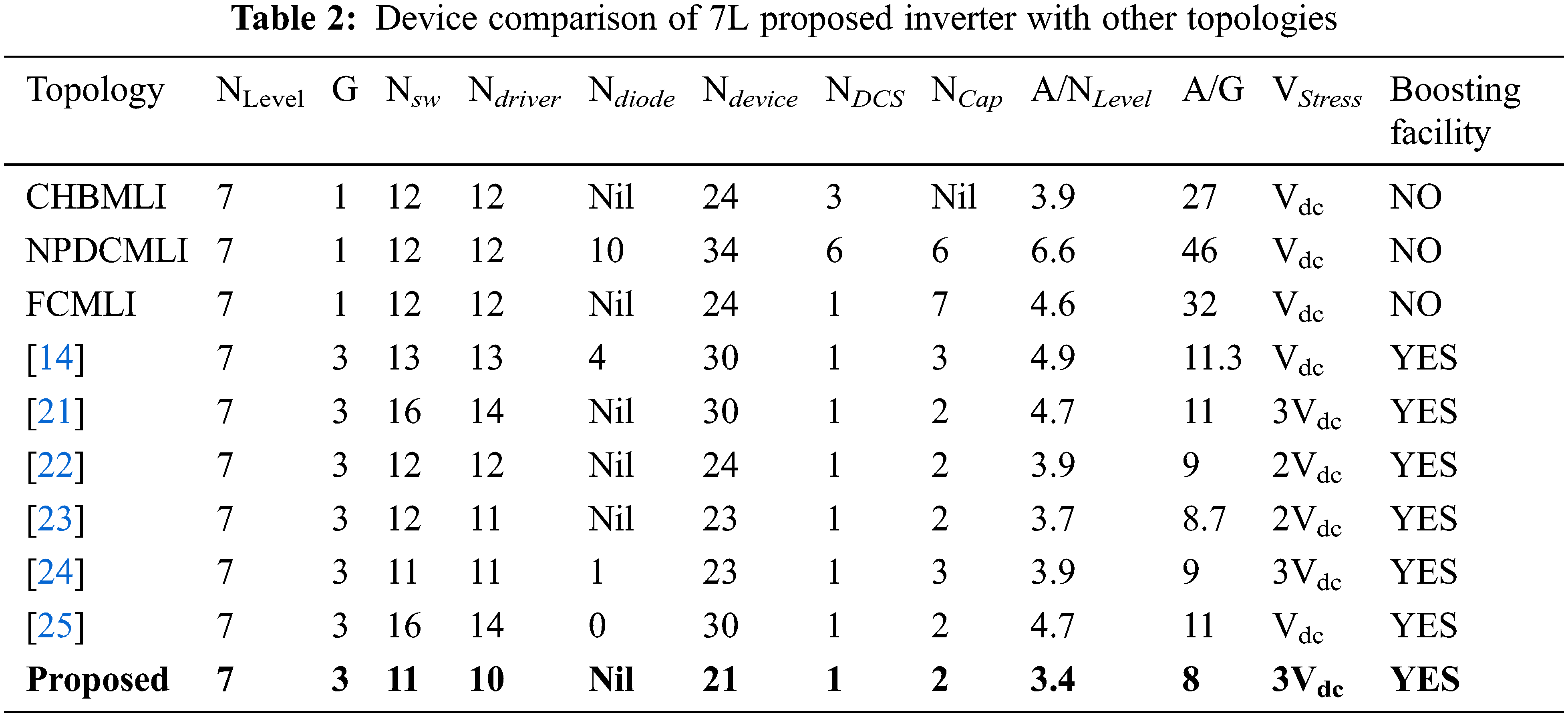
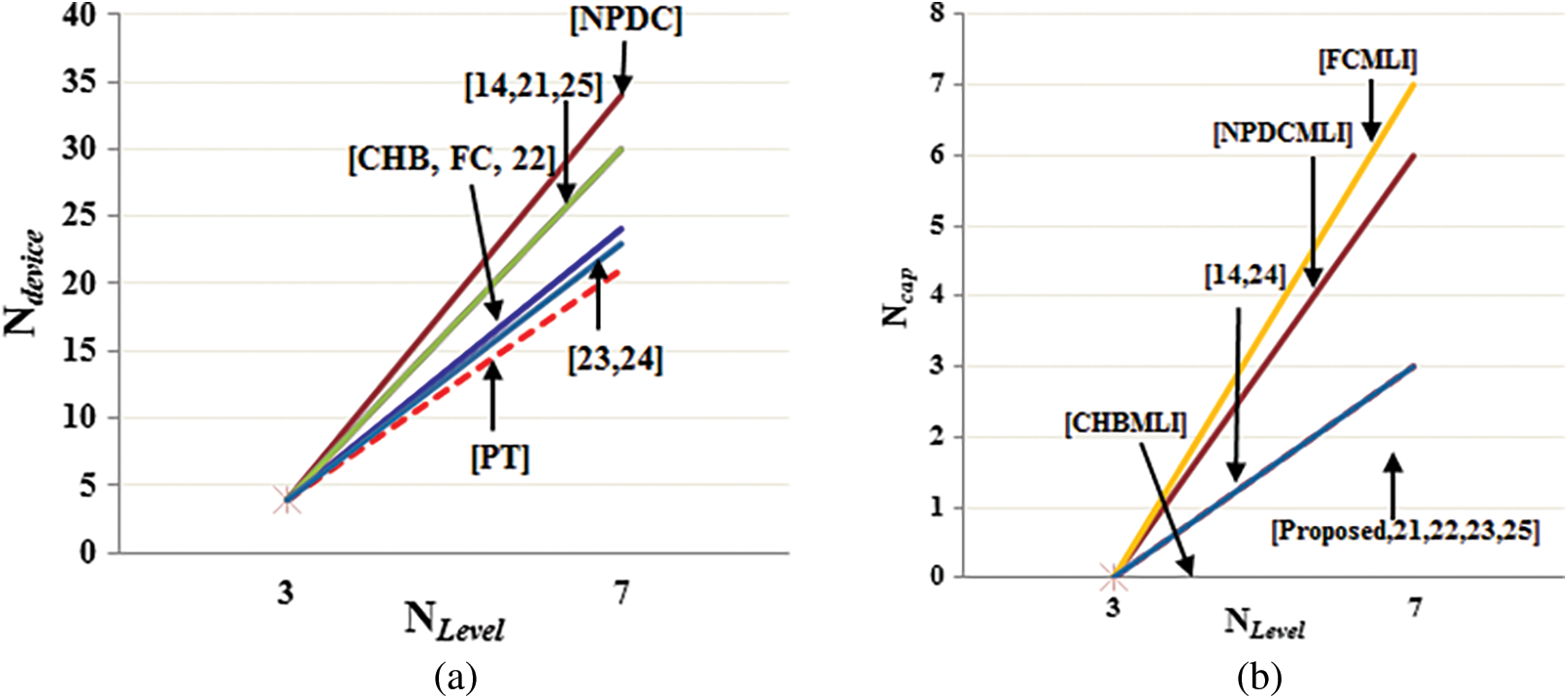
Figure 6: Comparison of output voltage levels with respect to (a) the total number of switching devices and (b) total number of capacitors
As seen in Fig. 7a, the total component per gain ratio (A/G) is also lesser in the suggested model than in other topologies.
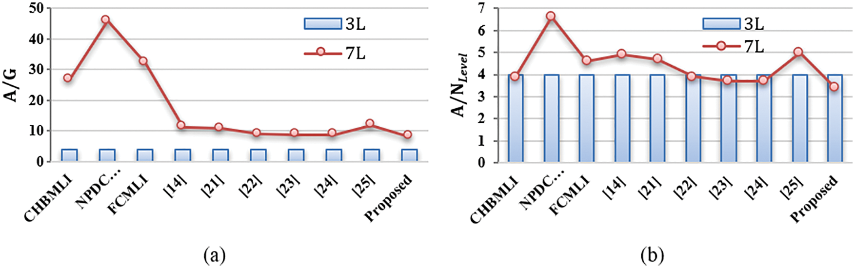
Figure 7: Comparison of required components with (a) gain factor and (b) per level factor
Similarly, as shown in Fig. 7b, the total component per level (A/NLevel) in the suggested structure is lesser than in other topologies.
5.1 Extension of the Proposed 7L Inverter
The cascaded arrangement of the suggested 7-level structure has been designed to produce the higher output voltage level, as illustrated in Fig. 8. N cascaded modules make up the structure. The proposed 7-level inverter topology is used in each module.
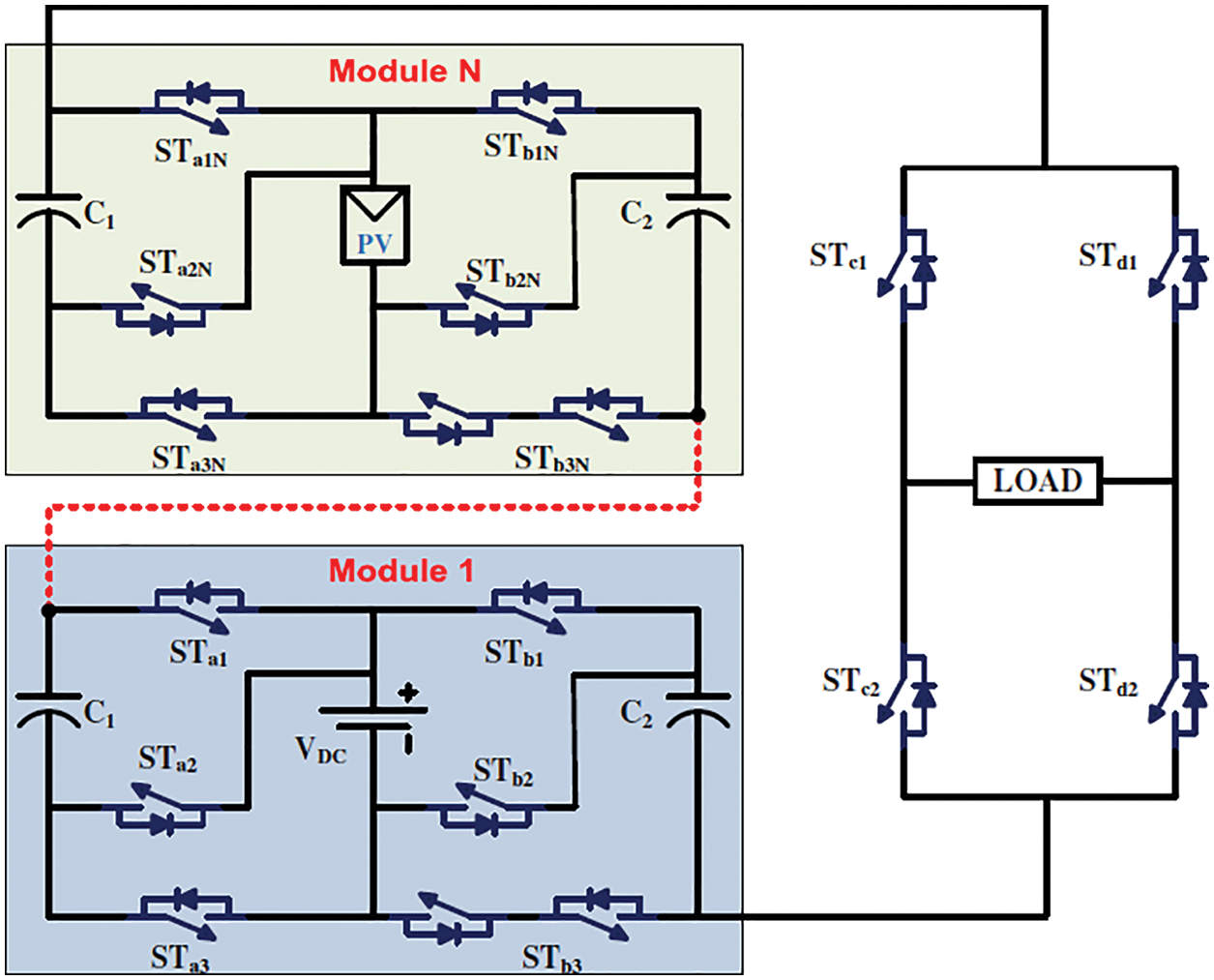
Figure 8: Proposed 7 L topology in a cascaded arrangement
Using (7N + 4) switches, 2N capacitors, and N input DC sources, the suggested structure can achieve (6N + 1) output voltage levels when all modules have the same magnitude of DC voltage sources. To replace the DC source, existing renewable resources such as photovoltaic (PV), fuel cell, and others can be employed. The advantage of the cascaded configuration is that it requires only one H-bridge for polarity switching, while the remaining modules are employed for voltage boosting.
6 Simulation and Hardware Prototype Results
The prototypical 7L inverter model has been designed and analyzed with the help of SIMULINK tool in terms of static and dynamic characteristics. The model has been tested with the load value of 2 kW at 0.8 lagging power factor and the simulated results are displayed in Fig. 9. The inverter delivers peak ac output voltage value of 300 V, fed from a 100 V DC source. Fig. 9 displays the waveform of output load voltage (Vout), current (Iout) and capacitor voltages (VC1 and VC2) for the connected load value of (R = 50 Ω and RL = 40 Ω + 100 mH). Thus, the simulated results ensure that the proposed model has thrice voltage boosting capability without adding additional components. Also, the two capacitor voltages are maintained constant around 100 V during charging and reduced up to 94 V during peak discharging for a load of 2 kW. This shows that the capacitor ripple voltage is lesser and hence it enhances the durability of the capacitor.
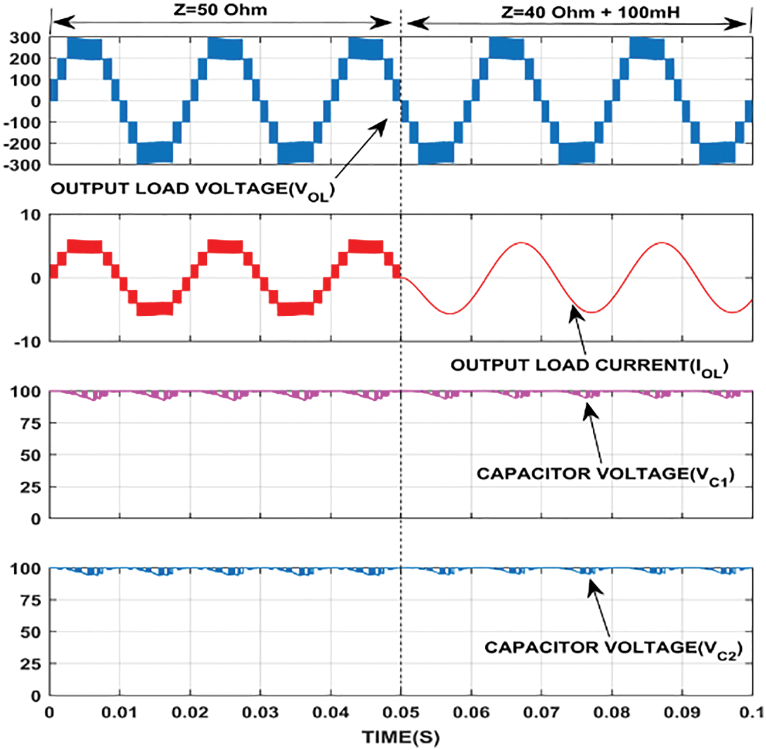
Figure 9: Simulated output waveform of the 7 L inverter with R = 50 Ω and RL = 40 Ω + 100 mH
The THD profiles of the proposed inverter can be seen in Fig. 10. Compared to the LS-CBPWM, the combined (SHE and LS-CB) PWM approach exhibits lower voltage harmonics by 19.62%. The lower order harmonics of 3rd and 5th are eliminated due to the influence of optimal switching angle generated through genetic algorithm.
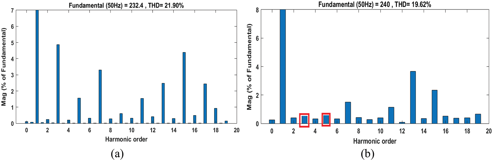
Figure 10: THD analysis (a) without SHEPWM (b) with SHEPWM reduced 3rd and 5th order
The dynamic load changing characteristics of the proposed model has been verified with two different values of loads (Z = 50 Ω and Z = 40 Ω + 100 mH) and is displayed in Fig. 9. It has been observed that the Vout waveform remains unaltered and the shape of the output current waveform alone changes due to inductive load change. Moreover, the change in load from Z = 50 Ω to Z = 40 Ω + 100 mH has reduced the ripple content across the capacitor voltage. The proposed 7-level inverter has been validated using a hardware archetype is shown in Fig. 11. TMS320F2812 module has been used to provide gate signals for the driver ICs. The switching algorithm is encoded in TMS320F2812 processor using code composer studio (CCS) software.
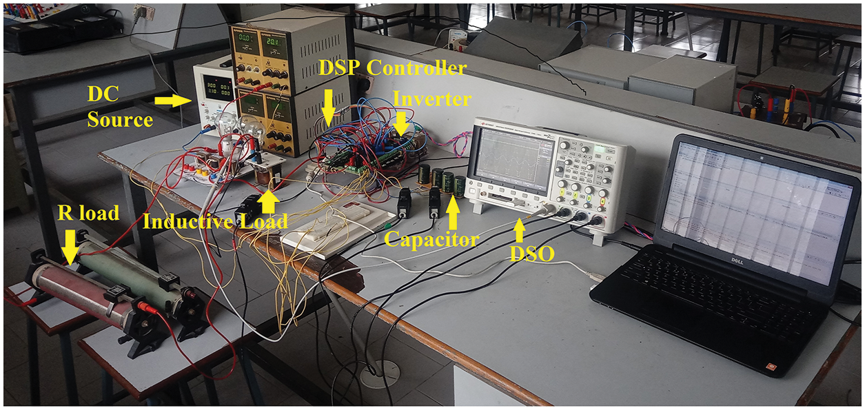
Figure 11: Hardware prototype
Tab. 3 presents the test evaluation parameters of the designed 7L single phase inverter prototype. The proposed model’s output load current and voltage waveforms are examined using a key sight DSO oscilloscope. The fluke meter is used to determine the load’s overall harmonic profile. The prototype is tested with a 90 V DC input, and the resulting capacitor voltage, load voltage, and current are shown in Fig. 12a. The seven voltage levels of (±90 V, ±180 V, ±270 V, 0 V) with a 5 A output current can be seen in Fig. 12a. The enlarged waveform of the prototype results with the current values of the capacitor is shown in Fig. 12b.
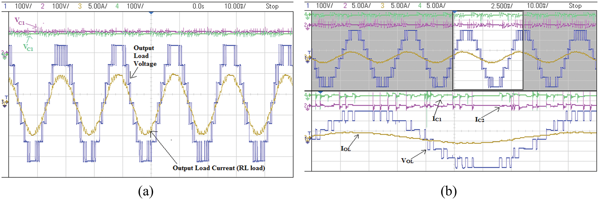
Figure 12: Experimental results; (a) RL load Z = 40 Ω + 100 mH with capacitor voltage and (b) RL load Z = 40 Ω + 100 mH with capacitor current in magnified waveform
Furthermore, the prototype characteristics are evaluated using Fluke 430-II meter and the test results of the 7 L inverter are shown in Fig. 13. The prototype is tested with an 85 V DC input voltage and a Z = 40 Ω +100 mH RL load. Output voltage and current waveforms are shown in Fig. 13a. The THD value is around 21% as shown in Fig. 13b, which is slightly higher than the simulated value. The both the capacitor voltage of VC1 and VC2 are shown in Figs. 13c and 13d respectively. Both the capacitors C1 and C2 maintain its voltage around 83 V. It shows that the self-balancing voltage technique provides better stability during peak loads. Thus, the prototype validates the simulated results.
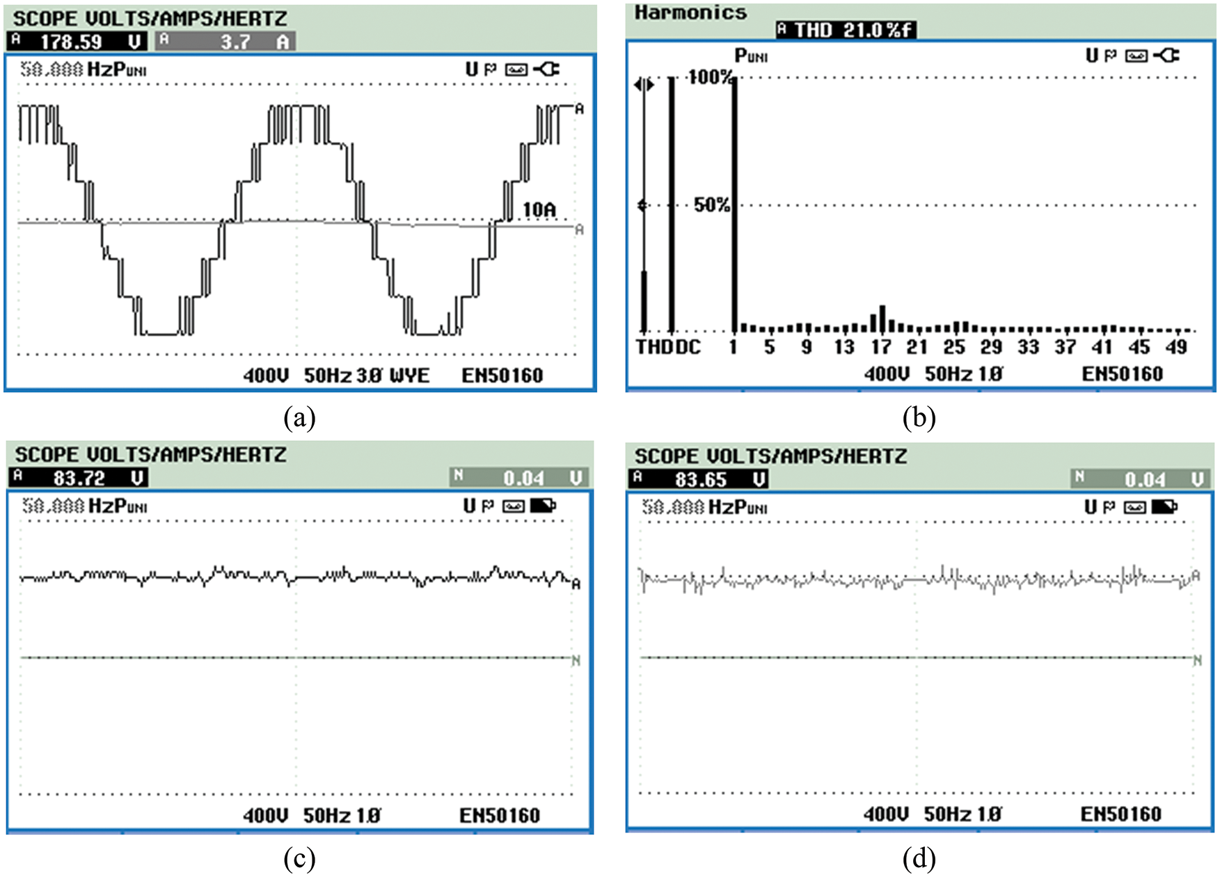
Figure 13: Experimental results in fluke meter: (a) Load voltage and current, (b) Total Harmonic Distortion (THD) (c) Capacitor voltage (VC1) and (d) Capacitor voltage (VC2)
A single DC sourced seven-level inverter using switched capacitor technique is proposed in this paper. The highlight of the proposed model lies in boosting the output voltage into three times that of input voltage. Inherently, with the use of two switched capacitors it could generate seven voltage levels with the minimum quantity of power switching devices and gate control circuits. The GA algorithm based SHEPWM has been used to eliminate the 3rd and 5th order harmonics. Similarly, the suggested inverter exhibits the advantage of self-balancing algorithm, which retains the capacitor voltage during vigorous load changes. Mathematical modeling for the various operating states with power loss calculation is described in this paper. A detailed comparative analysis, made with the relevant level generating MLIs reveals that proposed model has better boosting capability with reduced switching devices and voltage stress across the switches. The simulated results of the proposed inverter are validated through the experimental prototype which confirms its suitability for single isolated DC to AC conversion system.
Acknowledgement: The author with a deep sense of gratitude would thank the supervisor for his guidance and constant support rendered during this research.
Funding Statement: The authors received no specific funding for this study.
Conflicts of Interest: The authors declare that they have no conflicts of interest to report regarding the present study.
References
1. M. Malinowski, K. Gopakumar, J. Rodriguez and M. A. Perez, “A survey on cascaded multilevel inverters,” IEEE Transactions on Industrial Electronics, vol. 57, no. 7, pp. 2197–2206, 2010. [Google Scholar]
2. J. Rodriguez, S. Bernet, P. K. Steimer and I. E. Lizama, “A survey on neutral-point-clamped inverters,” IEEE Transactions on Industrial Electronics, vol. 57, no. 7, pp. 2219–2230, 2010. [Google Scholar]
3. H. Abu-Rub, J. Holtz, J. Rodriguez and G. Baoming, “Medium-voltage multilevel converters—State of the art, challenges, and requirements in industrial applications,” IEEE Transactions on Industrial Electronics, vol. 57, no. 8, pp. 2581–2596, 2010. [Google Scholar]
4. M. Vijeh, M. Rezanejad, E. Samadaei and K. Bertilsson, “A general review of multilevel inverters based on main submodules: Structural point of view,” IEEE Transactions on Power Electronics, vol. 34, no. 10, pp. 9479–9502, 2019. [Google Scholar]
5. R. Stala, “Application of balancing circuit for DC-link voltages balance in a single-phase diode-clamped inverter with two three-level legs,” IEEE Transactions on Industrial Electronics, vol. 58, no. 9, pp. 4185–4195, 2011. [Google Scholar]
6. A. Salem, H. Van Khang, K. G. Robbersmyr, M. Norambuena and J. Rodriguez, “Voltage source multilevel inverters with reduced device count: Topological review and novel comparative factors,” IEEE Transactions on Power Electronics, vol. 36, no. 3, pp. 2720–2747, 2021. [Google Scholar]
7. X. Xiang, X. Zhang, T. Luth, M. M. C. Merlin and T. C. Green, “A compact modular multilevel DC-DC converter for high step-ratio MV and HV use,” IEEE Transactions on Industrial Electronics, vol. 65, no. 9, pp. 7060–7071, 2018. [Google Scholar]
8. M. Kaliamoorthy, V. Rajasekaran, I. G. Christopher Raj and L. Hubert Tony Raj, “Generalised hybrid switching topology for a single-phase modular multilevel inverter,” IET Power Electronics, vol. 7, no. 10, pp. 2472–2485, 2014. [Google Scholar]
9. E. Babaei, S. Laali and Z. Bayat, “A single-phase cascaded multilevel inverter based on a new basic unit with reduced number of power switches,” IEEE Transactions on Industrial Electronics, vol. 62, no. 2, pp. 922–929, 2015. [Google Scholar]
10. H. Nasiri Avanaki, R. Barzegarkhoo, E. Zamiri, Y. Yang and F. Blaabjerg, “Reduced switch-count structure for symmetric multilevel inverters with a novel switched-DC-source submodule,” IET Power Electronics, vol. 12, no. 2, pp. 311–321, 2019. [Google Scholar]
11. C. Dhanamjayulu and S. Meikandasivam, “Implementation and comparison of symmetric and asymmetric multilevel inverters for dynamic loads,” IEEE Access, vol. 6, pp. 738–746, 2018. [Google Scholar]
12. S. Behara, N. Sandeep and U. R. Yaragatti, “Design and implementation of transformer-based multilevel inverter topology with reduced components,” IEEE Transactions on Industry Applications, vol. 54, no. 5, pp. 4632–4639, 2018. [Google Scholar]
13. O. Lopez-Santos, C. A. Jacanamejoy-Jamioy, D. F. Salazar-D’Antonio, J. R. Corredor-Ramírez, G. Garcia et al., “A single-phase transformer-based cascaded asymmetric multilevel inverter with balanced power distribution,” IEEE Access, vol. 7, pp. 98182–98196, 2019. [Google Scholar]
14. A. Lashab, D. Sera, T. Kerekes, Y. Terriche, A. Bouzid et al., “A cascaded H-bridge with integrated boosting circuit,” IEEE Transactions on Power Electronics, vol. 36, no. 1, pp. 18–22, 2021. [Google Scholar]
15. H. Matsumoto, Y. Shibako and Y. Neba, “Single-phase inverter with energy buffer and DC-DC conversion circuits,” IEEE Transactions on Power Electronics, vol. 32, no. 10, pp. 7615–7625, 2017. [Google Scholar]
16. M. Babaie, M. Sharifzadeh, H. Y. Kanaan and K. Al-Haddad, “Switching-based optimized sliding-mode control for capacitor self-voltage balancing operation of seven-level PUC inverter,” IEEE Transactions on Industrial Electronics, vol. 68, no. 4, pp. 3044–3057, 2021. [Google Scholar]
17. R. Vasu, S. K. Chattopadhyay and C. Chakraborty, “Seven-level Packed U-Cell (PUC) converter with natural balancing of capacitor voltages,” IEEE Transactions on Industry Applications, vol. 56, no. 5, pp. 5234–5244, 2020. [Google Scholar]
18. J. Choi and F. Kang, “Seven-level PWM inverter employing series-connected capacitors paralleled to a single DC voltage source,” IEEE Transactions on Industrial Electronics, vol. 62, no. 6, pp. 3448–3459, 2015. [Google Scholar]
19. B. Prathap Reddy, M. D. Siddique, A. Iqbal, S. Mekhilef, S. Rahman et al., “7L-SCBI topology with minimal semiconductor device count,” IET Power Electronics, vol. 13, no. 14, pp. 3448–3459, 2020. [Google Scholar]
20. A. Iqbal, M. D. Siddique, J. S. M. Ali, S. Mekhilef and J. Lam, “A new eight switch seven level boost active neutral point clamped (8S-7L-BANPC) inverter,” IEEE Access, vol. 8, pp. 203972–203981, 2020. [Google Scholar]
21. X. Sun, B. Wang, Y. Zhou, W. Wang, H. Du et al., “A single DC source cascaded seven-level inverter integrating switched-capacitor techniques,” IEEE Transactions on Industrial Electronics, vol. 63, no. 11, pp. 7184–7194, 2016. [Google Scholar]
22. M. D. Siddique, S. Mekhilef, N. M. Shah, J. S. M. Ali, M. Seyedmahmoudian et al., “Switched-capacitor-based boost multilevel inverter topology with higher voltage gain,” IET Power Electronics, vol. 13, no. 14, pp. 3209–3212, 2020. [Google Scholar]
23. M. D. Siddique, S. Mekhilef, N. M. Shah, J. S. M. Ali and F. Blaabjerg, “A new switched capacitor 7L inverter with triple voltage gain and low voltage stress,” IEEE Transactions on Circuits and Systems II: Express Briefs, vol. 67, no. 7, pp. 1294–1298, 2020. [Google Scholar]
24. M. N. H. Khan, M. Forouzesh, Y. P. Siwakoti, L. Li and F. Blaabjerg, “Switched capacitor integrated (2n + 1)-level step-up single-phase inverter,” IEEE Transactions on Power Electronics, vol. 35, no. 8, pp. 8248–8260, 2020. [Google Scholar]
25. S. Lee, “A single-phase single-source 7-level inverter with triple voltage boosting gain,” IEEE Access, vol. 6, pp. 30005–30011, 2018. [Google Scholar]
26. S. S. Lee, B. Chu, N. R. N. Idris, H. H. Goh and Y. E. Heng, “Switched-battery boost-multilevel inverter with GA optimized SHEPWM for standalone application,” IEEE Transactions on Industrial Electronics, vol. 63, no. 4, pp. 2133–2142, 2016. [Google Scholar]
Cite This Article
 Copyright © 2023 The Author(s). Published by Tech Science Press.
This work is licensed under a Creative Commons Attribution 4.0 International License , which permits unrestricted use, distribution, and reproduction in any medium, provided the original work is properly cited.
 Downloads
 Citation Tools