
 Submit a Paper
 Propose a Special lssue
 Open Access
ARTICLE

Reconfigurable Logic Design of CORDIC Based FFT Architecture for 5G Communications
1 Department of Electronics and Communication Engineering, Anjalai Ammal Mahalingam Engineering College, Thiruvarur, 614403, Tamilnadu, India
2 Department of Electronics and Communication Engineering, Rajalakshmi Engineering College, Chennai, 602105, Tamilnadu, India
* Corresponding Author: C. Thiruvengadam. Email:
Intelligent Automation & Soft Computing 2023, 36(3), 2803-2818. https://doi.org/10.32604/iasc.2023.030493
Received 27 March 2022; Accepted 27 April 2022; Issue published 15 March 2023
 View Full Text
 Download PDF
Abstract
There are numerous goals in next-generation cellular networks (5G), which is expected to be available soon. They want to increase data rates, reduce end-to-end latencies, and improve end-user service quality. Modern networks need to change because there has been a significant rise in the number of base stations required to meet these needs and put the operators’ low-cost constraints to the test. Because it can withstand interference from other wireless networks, and Adaptive Complex Multicarrier Modulation (ACMM) system is being looked at as a possible choice for the 5th Generation (5G) of wireless networks. Many arithmetic units need to be used on the hardware side of multicarrier systems to do the pulse-shaping filters and inverse FFT. The main goal of this study is to adapt complex multicarrier modulation (ACMM) for baseband transmission with low complexity and the ability to change it. We found that this is the first reconfigurable architecture that lets you choose how many subcarriers a subband has while still having the same amount of hardware resources as before. Also, under the new design with a single selection line, it selects from a set of filters. The baseband modulating signal is evaluated and tested using a Field-Programmable Gate Array (FPGA) device. This device is available from a commercial source. New technology outperforms current technology in terms of computational complexity, simple design, and ease of implementation. Additionally, it has a higher power spectrum density, spectral efficiency, a lower bit error rate, and a higher peak to average power ratio than existing technology.Keywords
Recent field tests of 5G wireless communication have been conducted. 5G use cases are divided into massive Machine Type Communications (mMTC), enhanced Mobile Broadband (eMBB), and Ultra-reliable and Low Latency Communications (uRLLC) [1]. Each of these groups relies on the air interface. Lengthy symbol duration is appropriate for delay-tolerant mMTC but not for latency-sensitive uRLLC.The doubly dispersive channel also limits the symbol duration in eMBB. For 5G wireless communications, orthogonal/nonorthogonal and synchronous/asynchronous multicarrier waveforms are being investigated [2]. Multiservice provisioning necessitates using a large number of subbands and subband filtering through a single air interface. Cyclic-prefix-based Orthogonal Frequency Division Multiplexing (OFDM) is incompatible with multiservice provisioning because of neighbouring sidebands’ significant out-of-band emission level. Although it is preferred due to its reduced sidelobe suppression, its long filter length limits its effectiveness for quick burst traffic. On the other hand, Universal Filtered Multicarrier (UFMC) has a small amount of out-of-band spectrum leakage and a low filter length for successive subcarrier filtering, and it combines the benefits of OFDM and Filter Bank Multicarrier (FBMC) with a lower filter length [3–5]. Since UFMC minimizes time-frequency misalignment, it is a strong competitor for 5G multicarrier waveforms. A block schematic of a waveform modulator is shown in the Fig. 1.
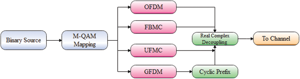
Figure 1: The block diagram of a waveform modulator
However, choosing a pulse-shaping filter is critical in UFMC to limit sidelobe power to adjacent subbands. This filter’s sidelobe fall rate is extraordinarily sluggish (0 dB/octave), resulting in significant spectrum leakage to neighbouring subbands [6,7]. Jiang et al. [8] proposed an adaptive interference cancellation approach with cancellation subcarriers injected at the narrow guard bands to facilitate filter selection and Yarrabothu et al. [9] proposed alternate waveforms for the UFMC pulse-shaping filters based on transmitter channel state information. UFMC systems provide much flexibility in subcarrier and filter length choices and architectural reconfigurability. Because of end-device power and resource constraints, computational complexity in hardware implementation becomes important in UFMC systems. In reality, the most resource-intensive components in UFMC systems are the Inverse Discrete Fourier Transform/Inverse Fast Fourier Transform (IDFT/IFFT) and pulse-shaping filters [10,11]. For this reason, proposed a 64-point IFFT instead of the more common 1024-point IFFT. In contrast, the 64-point IFFT block was used in, followed by a 1024-point IFFT upsampling. Consequently, the computational complexity [12] of is lower than that of existing architectures.
Nowadays, [13] by Jarfi and others propose a hardware-efficient architecture that enables the UFMC transmitter’s IFFT size, filter length, and spectrum shifting parameters to be freely set. The approach, as mentioned earlier, eliminated duplicate radix-2 Decimation-In-Time (DIT) butterfly operations, leading to a significant reduction in filtering hardware complexity. When a 10-MHz Long-Term Evolution (LTE) channelization standard was used, the spectrum shifting procedure needed a few memory units, one multiplier, and one adder. [14] provided a more detailed design that complied with the timing constraints of 10-MHz LTE channelization, provided a more complex technique that adhered to the timing constraints of 10-MHz LTE channelization, with an FPGA implementation of the UFMC transmitter. However, the design methodologies for changing the filter type and length in the UFMC transmitter remain unknown, as do the read-only memory (ROM)-based approaches for directly storing the sine/cosine values for the IDFT/IFFT unit and pulse-shaping filter sample points [15,16]. Additionally, the IDFT/IFFT unit and the pulse shaping filters in UFMC systems need computational operations. The most recent design in [16] exploits data and process level pipelining to minimize computing complexity and increase operating frequency throughout the UFMC transmitter. The sine/cosine terms of the twiddle factors imposed constraints on the number of subcarriers per subband and the duration of the pulse-shaping filter for each subband. Thus, one of the significant challenges in 5G UFMC systems is creating a reconfigurable and hardware efficient baseband transmitter with the required pulse-shaping filter. However, there are no studies on the quantification inaccuracy of a reconfigurable UFMC architecture.
This Work’s Contribution
The following are the present work’s significant contributions.
1) We want to develop a programmable baseband UFMC transmitter. We create a prototype of the suggested design and test it on a commercially available FPGA chip.
2) The maximum number of subcarriers that may be employed in the proposed architecture is 2(d-1), which equals the architecture’s data length. Use more than one subcarrier per subband for the UFMC transmitter.
3) Using base-band modulation, we investigate how the closeness of an approximate and the comfort level with truncation are affected by a fixed-size representation of the data-path width.
In fourth-generation broadband systems that have long depended on Orthogonal Frequency Division Multiplexing (OFDM), some of its drawbacks have spurred academics to examine other modulation methods that might improve global performance in the next generation [17]. These alternatives possess some intriguing characteristics, even if they do not constitute a paradigm leap in technology on the scale of the transitions from Frequency Division Multiple Access (FDMA) to Code Division Multiple Access (CDMA) or CDMA to OFDM. While these innovative modulations may not completely replace OFDM as a general-purpose communication paradigm that works well in most communication situations, they may be beneficial in some applications or circumstances. Here, Filter Bank Multi-Carrier (FBMC), Universal Filtered Multi-Carrier (UFMC), and Generalized Frequency Division Multiplexing (GFDM) [18] will be examined in this research. Consequently, each of them has been designed to overcome some of OFDM’s shortcomings, making them suitable for particular applications.
By copying the final part of the signal at the beginning (cyclic prefix), OFDM reduces Inter-Symbol Interference (ISI) and makes the signal more resistant to channel delays Fast Fourier transform (FFT). Although OFDM is effective in most situations, it is not always easy to use.
Out-of-band radiation is the most severe flaw of OFDM, causing a lot of noise. Each subcarrier’s waveform is Sinc shaped. This type produces enormous secondary lobes. These lobes extend beyond the data transmission frequency range, resulting in worse global spectral efficiency. The secondary lobes of OFDM-Sincs are likewise relatively strong, emphasizing the requirement for accurate synchronization. Symbol mismatches destroy orthogonality and accentuate secondary lobe effects. A more extended cyclic prefix may help reduce interference but at a cost.
Recently, various modulation techniques have addressed obstacles such as high Peak to Average Power Ratio (PAPR) and phase and frequency noise susceptibility [19,20]. They are planned for usage in 5G technology (5th generation).
2.2 Filter Bank Multi Carrier Modulations (FBMC)
Recently, interest in Filter Bank Multi-Carrier modulation (FBMC) as a viable alternative to OFDM has increased significantly. FBMC is an improvement, particularly in spectrum efficiency and severe time restrictions. As with OFDM in general, each sub-carrier is filtered to minimize side-lobes and inter-carrier interference and the out-of-band effect of the global allotted bandwidth. As a result, the CP is not required, allowing for high data rates but complicating support for Multiple-Input and Multiple-Output (MIMO) systems. Due to the massive size of the filter, short-term transmissions are inefficient. The primary advantage of FBMC is the overlapping of surrounding subcarriers, which makes it resistant to synchronization problems [21]. The cost of trade is computational complexity. At the same time, some modern approaches employ FFT and vary its output, the number of procedures required for transmission and reception rises.
2.3 Universal-Filtered Multi-Carrier (UFMC)
Unlike FBMC, which filters individual OFDM sub-carriers, Universal-Filtered Multi-Carrier filters groups of sub-carriers. Unlike the FBMC filter, the length of the filter may be reduced by grouping sub-carriers. Each group receives its own IFFT, and the output is filtered identically (with the same filter, or even different filters can be applied if desired). As seen in Fig. 2, the final UFMC signal is generated by adding the filtering outputs. Individual filtering on each group may significantly reduce out-of-band spectral emissions. Additionally, sub-band filtering decreases the guard interval between sub-bands and the filter length, making it suitable for sending brief bursts of data [22]. Since UFMC has a higher spectral efficiency than OFDM, it is a superior option.
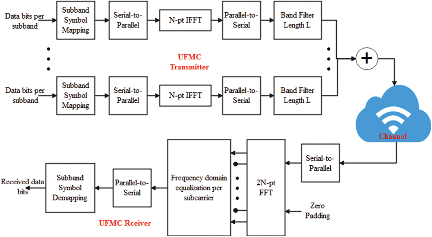
Figure 2: Block diagram UFMC transceiver
3 Proposed Adapting Complex Multicarrier Modulation
The simplicity and cheap cost make it an excellent choice for next-generation cellular networks, but complicated multicarrier modulation methods need that signals sent be genuine and positive. Because OFDM has inherent complex values, standard OFDM cannot be employed. To maintain the primary properties inherent in the original modulation while transmitting just a single actual component, many OFDM modifications have been proposed in recent years. If Hermitian Symmetry (HS) is applied to the inverse Fourier transform’s (IFFT/FFT) input, the output is real, but it requires twice the number of IFFT/FFT points in transmission and reception, which increases computational complexity, demands more power, and necessitates larger chip dimensions. This procedure has traditionally been followed. In order to limit negative magnitudes, many strategies have been suggested. These include either adding the equivalent DC bias to increase global power or simply clipping negative values to zero, which results in undesirable noise. Other approaches, such as the Hartley transform, have been proposed to avoid the needless IFFT and FFT computations. This transform, however, has the peculiarity of working in real space while restricting the input modulations to only being real, preventing us from using high-density constellations like M-ary Quadrature Amplitude Modulation (M-QAM). Sequentially, modern methods that split and transmit the complex-valued OFDM’s real (Re) and imaginary (Im) portions have achieved intriguing results.
As described in [22], we will use the methods described therein to decouple the real and imaginary components of the default complex OFDM-generated signal (as well as the inheritance FBMC, UFMC, and GFDM when dealing with each of them) and to juxtapose the two in the time domain. This method beats traditional OFDM systems while sacrificing just a minimum capacity in terms of cost and complexity. Our goal is to execute as few operations as possible in the RRHs. Our strategy helps us achieve that goal by outsourcing the complicated signal processing and forwarding to the data center-based baseband units. Suppose the RRH is configured to receive the FBMC/UFMC/GFDM wireless signals using this type of scheme. In that case, these signals can be transmitted through intensity-modulated fronthaul fibers to the BBU in a seamless manner with only minimal processing (separating the complex and real parts and sending them sequentially).
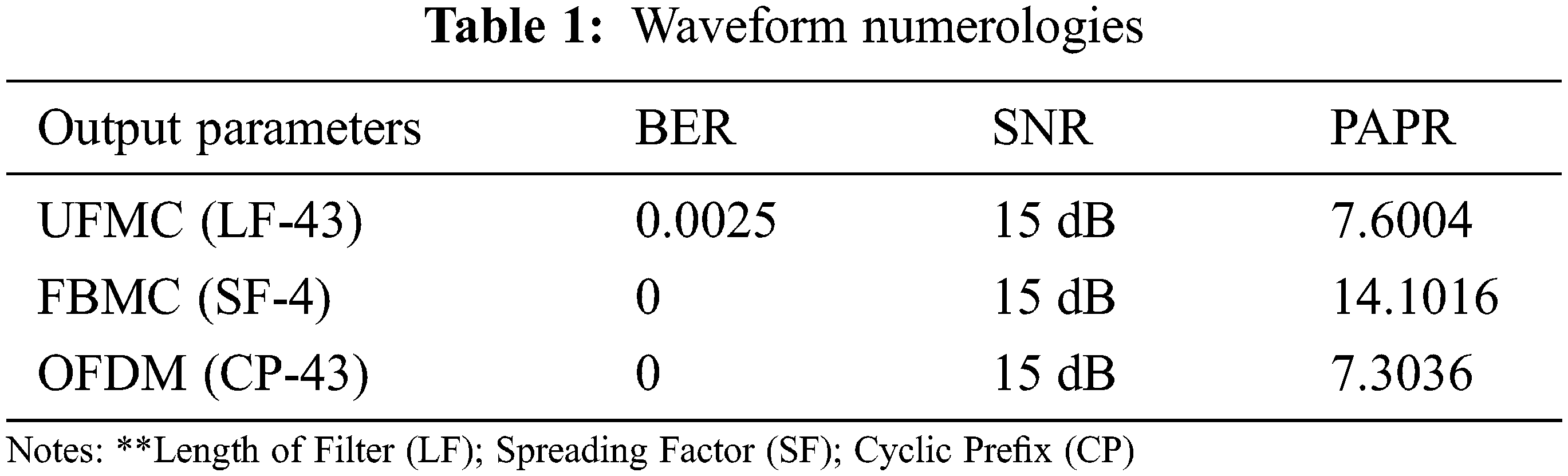
The physical layer candidates are compared against 5G as part of the project. Because the 5G standard hasn’t been finalized, it uses a variety of modulation methods. OFDM, FBMC, and UFMC modulation schemes are compared here. Simulating these modulations with an FFT length N = 512 and Bits per Subcarrier = 4 is necessary to compare. Periodograms of OFDM and UFMC baseband signals are shown together in Fig. 3 in a situation where these waveforms share a part of the spectrum band. For all digital modulation, 16-QAM constellations were employed. Bit Error Rate (BER) vs. Signal-to-Noise Ratio (SNR), PAPR, and the power spectral density were all considered. MATLAB is used to implement the design into analysis the output parameter is shown in Table 1.
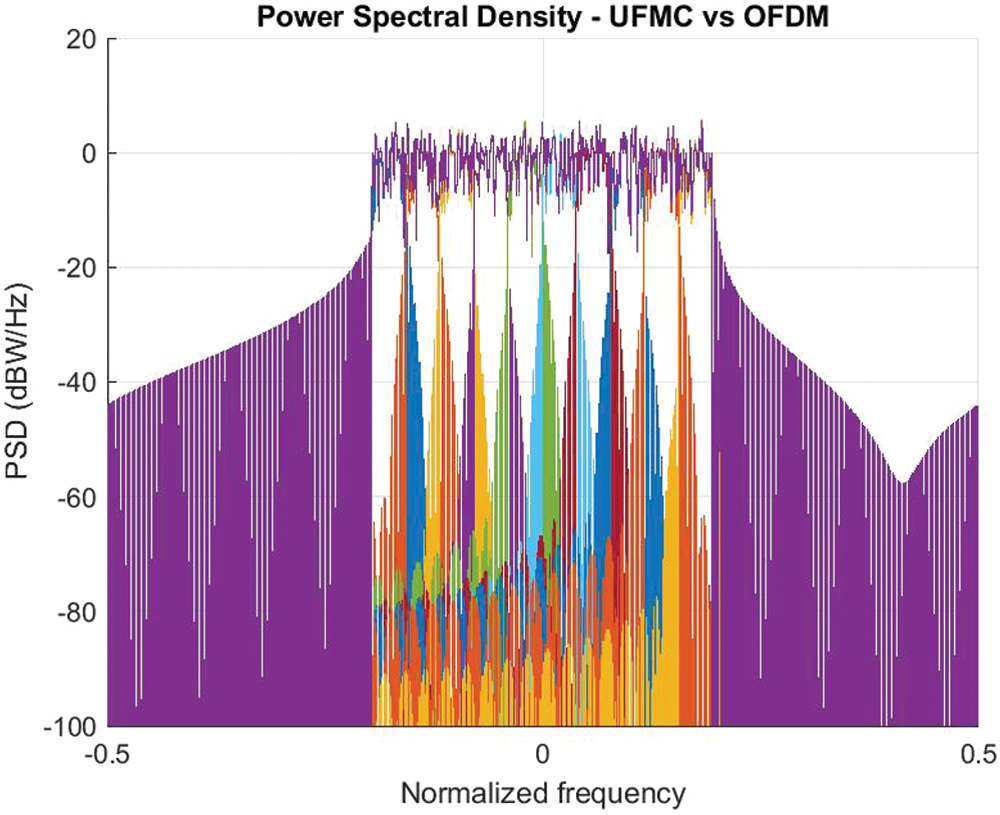
Figure 3: UFMC vs. OFDM baseband signal periodograms
The Fast Fourier Transform (FFT) is a discrete Fourier transform variant of the Discrete Fourier Transform (DFT). By lowering the time and effort necessary to calculate the DFT, the Fast Fourier Transform (FFT) decreases its computational complexity. The butterfly diagram in Fig. 4 illustrates this method, which converts time domain data to frequency domain data [23].
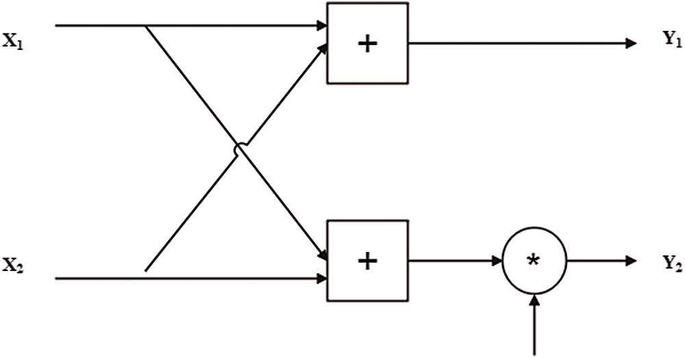
Figure 4: The basic 2-Point butterfly computation
This computing technique improvement results in increased processing components while retaining the first-in, first-out process size. Parallel pipelined FFT requires less electricity due to lower frequency. FFT uses improved Coordinate Rotation Digital Computer (CORDIC) to build FPGA [24,25]. The expanded optimum CORDIC technique demands a lot of math in the initial step. First, input data streams are created. Both storage units communicate information. It classifies the available coefficients as even (coefficient 1) or odd (coefficient 2). Then an Approximate CORDIC. Multiplexer Based Approximate Full Adder-Repetitive Iteration CORDIC (MAFA-RICO) creates FFTs rather than factoring. This approach replaces multiplication in all shift operations. Comprised of four real multipliers, a subtractor, and an addition, this recommended technique improves the area, delay, and energy utilization [26,27].
The performance of the proposed MAFA-RICO may be investigated utilizing an FFT-based design on FPGAs [28]. A CORDIC approximation technique minimizes hardware complexity by reducing the number of adders. The new angle set has fewer design additions. This design decreases the number of repetitions, the amount of space required, and the energy consumed. Compared to prior systems, the approximation CORDIC architecture has lower latency, less hardware overhead, and needs adders [29,30]. It is feasible to approximate the critical route (speed) and power consumption. For power utilization, the speed with the fewest flaws is crucial. MAFA-based cost and depth values may be created using the online version’s cost and depth adder options, and the MAFA’s bit-level description may be used to compute the critical route. The use of the MAFA as a basis enables an extremely efficient rotation.
The MAFA-RICO technique [30] may be used to create a reconfigurable FFT processor without storing complicated twiddle factor values in memory blocks. A reprogrammable FFT processor is shown in Fig. 5. It saves input data in RAM and transfers read data to the butterfly unit, where it is mixed with data from the CORDIC and FFT butterfly units. The read/write address of the address generator is used to deliver data to RAM. As a result, the FFT butterfly unit reads data. The data from the MAFA-RICO butterfly unit is transmitted to the rotatable CORDIC block.
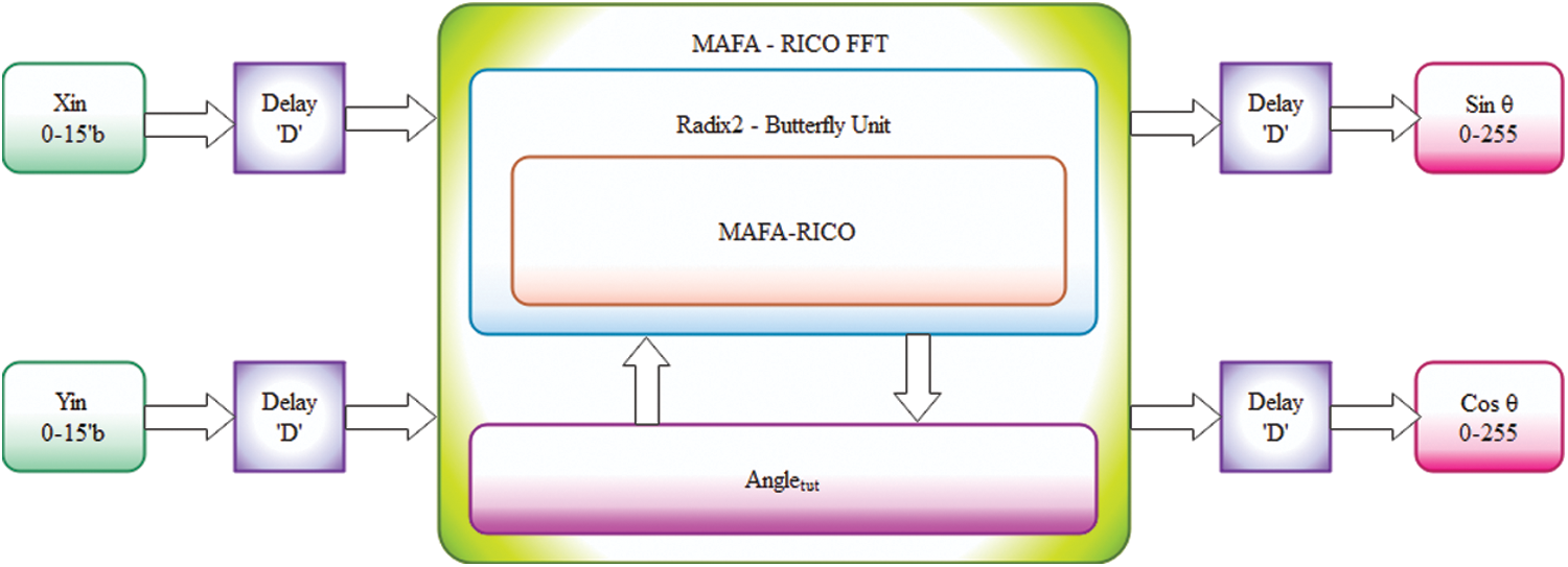
Figure 5: Proposed MAFA-RICO based FFT architecture
4.1 Approximate ADD-SUB Circuit
Instead of having a specific model, inexact systems may be used to prepare all contract portions more efficiently. Because low-execution setups are more likely to include known faults, the superior design may use theoretical findings rather than idealized outcomes. Compared to a unit’s efficiency and inaccurate operation’s speed was more susceptible to competence than accuracy [31]. It uses inexact arithmetic units to perform more frequent but longer floating-point delay operations. Compared to other approximation approaches, this one is chosen because it provides the least uncertainty and has two errors. Each block of the Ripple Carry Adder (RCA) uses the full adder’s approximation mechanism [32].
a) Multiplexer Based Approximate Full Adder-I (MAFA1)
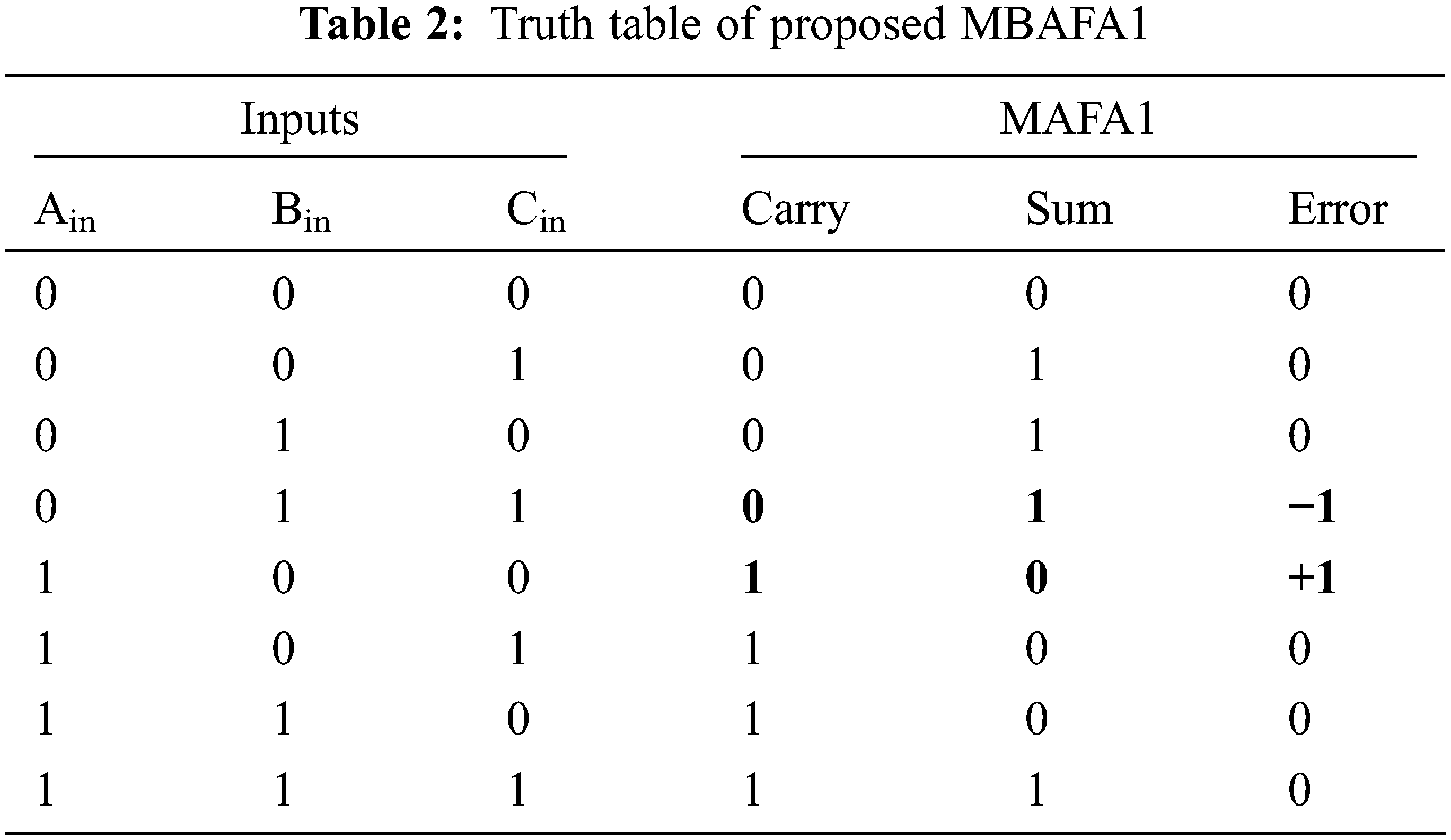
The proposed MAFA1 is based on the logic formulations in Eqs. (1)–(4), and it has two faults in eight instances [33]. MAFA1 has four components such as 1) approximate Full Adder (FA) carry generation is performed with a minimum critical path delay and error; 2) approximate Half Adder (HA) sum generation uses the sum of two inputs; 3) approximate half adder carry generation uses the product of two inputs; 4) approximate full adder sum generation is performed by selecting one of the approximate HA. If Approximate FA Carry equals “0,” the Approximate HA Sum output is picked; otherwise, the Approximate HA Carry output is selected.
Fig. 6 depicts the MAFA1 gate-level design, including six fundamental logic gates used in the sum logic construction. All inputs (Ain) are allocated a carry output to reduce node capacitance and speed up the carry propagation channel computations. There is less carry delay in the MAFA1 design than the overall output delay. Errors in carry output result in incorrect values being formed instead of correct values being produced overall, decreasing the error distance value to a value of 1, as seen in Tab. 2.
b) Multiplexer Based Approximate Full Adder-II (MAFA2)
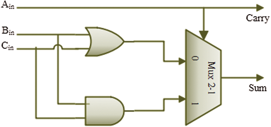
Figure 6: Gate-level architecture of proposed MBAFA1
An approximation full adder-II based on a four-unit multiplexer (MAFA2) is described in Eqs. (5)–(8) [33]. Four phases are involved in the logic operations: 1) a two-cascaded approximate half adder sum is generated by the sum of the three inputs. 2) The creation of half adder carry is stated as the product of two inputs. 3) An adder’s carry may be approximated by multiplying two inputs. 4) The approximate full adder sum is generated by choosing either the Approximate HA Sum output or the “Cin” input. If Approximate FA Carry equals “0,” the Approximate HA Sum output is chosen; otherwise, the Approximate FA Sum output is set to “Cin.”
There are seven fundamental logic gates in the proposed MBAFA-II logic, as shown in Fig. 7. The sum logic formulation uses six basic logic gates, whereas the carry generation approach uses one basic logic gate. Carry output delay is shorter than total delay in the suggested system. There is a one-to-one reduction in error distance as shown in Tab. 3 if an error is detected on a multiplexer input instead of selecting a correct value on a multiplexer output. Carry propagation is slowed down by a single logic gate delay in the MAFA2 design.
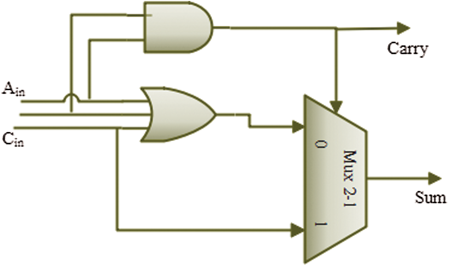
Figure 7: Gate-level architecture of proposed MBAFA-II
The accurate 16-bit MAFA1 calculation makes use of a typical RCA-based structure. At the same time, Fig. 8 depicts a parallel approximation adder for use in the inaccurate portion [33,34]. The Key advantages of MAFA1 are that the conventional addition procedure is done from the Last Significant Bit (LSB) of the inaccurate component to Most Significant Bit (MSB) of an accurate component. In contrast, traditional designs consider the exact part’s computing delay. Fig. 9 show that 16-bit MAFA2 with approximation modules is recommended in the inaccurate part. ‘I’ varies from 0 to 7 in the inaccurate part. Hence each approximation cell in that part has its carry propagation input, given by Ci + 1 = Ai & Bi. When designing a 16-bit MAFA2 processor, the critical path delay is the sum of one and a 4-bit standard RCA delay. While using a MAFA-I and MAFA-II for n = 16 adder then the accuracy of the adder is 99.92 and 99.85 respectively.
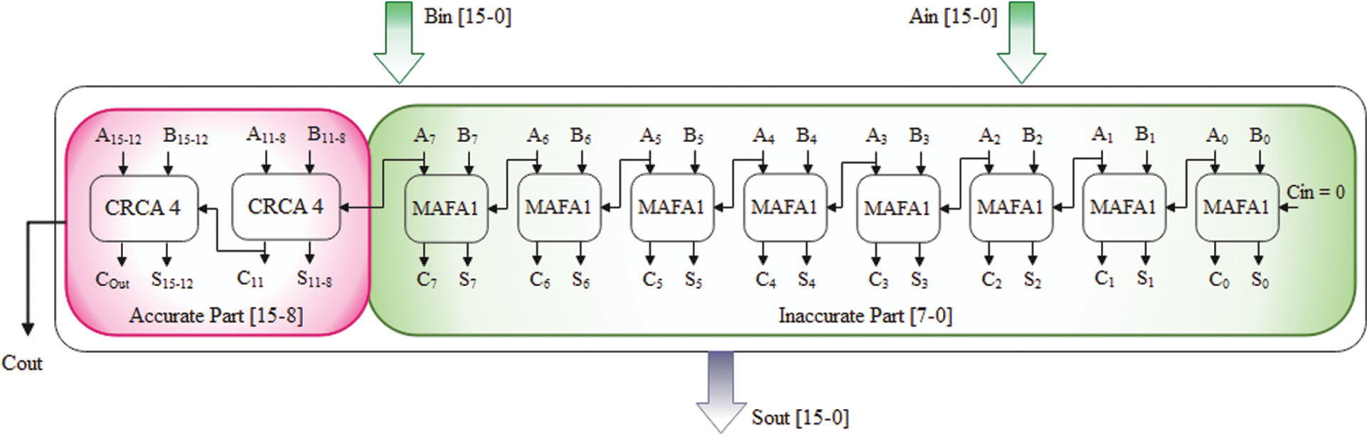
Figure 8: Block diagram of proposed 16-bit MAFA1
Figure 9: Block diagram of proposed 16-bit MAFA2
4.2 Proposed MAFA-RICO Algorithm
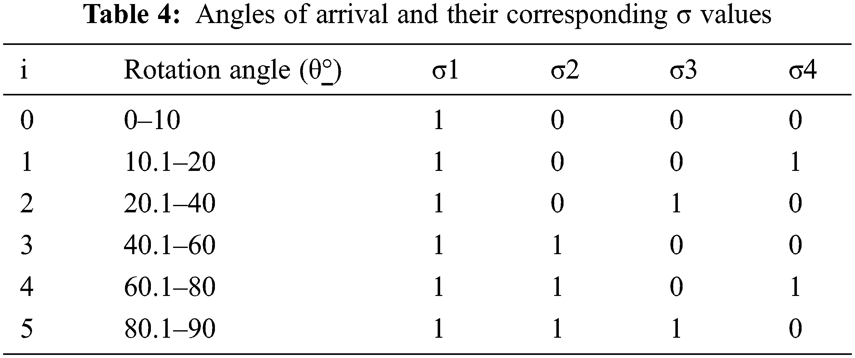
The proposed MAFA-RICO pseudocode rapidly computes the sine/cosine of the input angle (θ). Before identifying the direction of micro-rotation (σ), the input angle (θ) is compared to algorithm-defined thresholds (tθ: t11, t21, t41, t61, and t81 i.e., 11°, 21°, 41°, 61° and 81° respectively). Also computed are the shift values (R11 and R21) required to determine the sine/cosine value of the input [35]. The above values serve as cutoff values for determining sine and cosine based on Tab. 4. Diverse sets of angles have varying weights for the direction of microrotation. A new set is created for each significant change in the angle’s associated sine or cosine value from one set to the next. The following sections describe the architecture of the proposed algorithm.
When computing sine/cosine, the proposed MAFA-RICO (low power multiplexed approximate adder-based repeated iteration CORDIC) algorithm utilizes an arc-shaped route rotation (see Fig. 10). The iteration cycle for this design is restricted to five iterations to keep power consumption low while retaining sufficient efficiency. In this circumstance, repeated iterations result in a twice-repeated iteration for architectural evaluations. Despite the non-iterative nature of the architecture, the 16-bit add-sub unit incorrectly repeats one of these cycles. The recurrence of that particular condition implies the exact rotation that may be accomplished rather than the primary sense of the term refers. It calculates in real-time across all iterations, obviating the necessity for information. In Eq. (9), outputs such as mout, nout, and min, nin are defined as inputs, although the input and output vector is supplied independently. Iterations of component scaling are consistent with sl_ft, and micro-rotation of the path is μ0, μ1, μ2, μ3, and μ4.
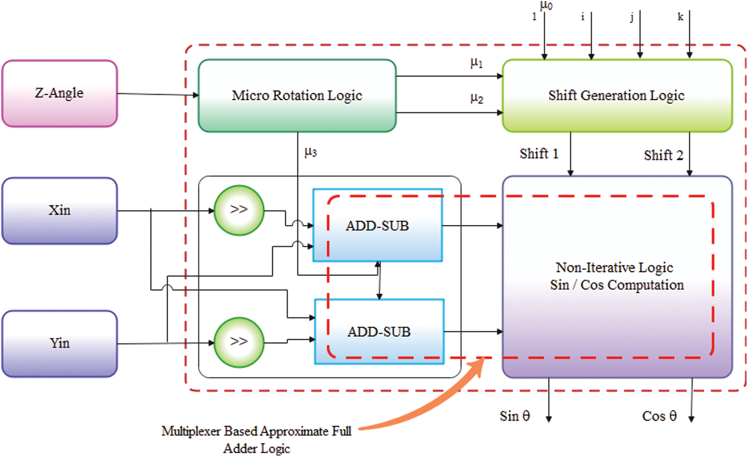
Figure 10: Multiplexer based approximate adder based repetitive iteration CORDIC (MAFA-RICO)
i) Micro-Rotation Generation
Accurate estimation μ is crucial for obtaining a superior quality standard. Although it is feasible to design an input θ based comparator and logic circuit that utilizes micro-rotation estimates of μ1, μ2, and μ3, the input threshold is defined by each entry. It relies on the angle input (i.e., t11, t21, t41, t61, and t81 all coincide with the angle input). The comparators’ outcomes (logic ‘high’) are set to the θ < tθ present. Shift logic is used to accomplish microrotation and non-iterative reasoning to compute sin and cos. Eq. (10) consider how −1 and 1 relate to the constraints imposed by the micro-rotation design when solving for μ1.
It has also been found and registered that micro-rotation may be used for μ1 and μ2.
ii) Shift Generation Logic
Logic for shifting levels must be specified in advance to determine the complexity to be shifted by the mout and nout. The contributions to shifting logic are μ1 and μ2, whereas the outputs are Shift 1 and Shift 2.
ii) Non-Iterative Computation Logic
The proposed approximate inaccurate technique Non-Iterative function eliminates the need for iteration on information 0, 1, and 2. It holds sin(θ) and cos(θ) values for the input stage. The move unit’s shift values are used to shift the output mout and nout, then calculate sin(θ) and cos(θ) using 16-bit approximate adder-subtractor.
4.3 Principle Operation of MAFA-RICO
The following are the MAFA-RICO-approximated architectural functions [36]:
1. Fig. 8 illustrates how the angle limit ‘t’ is used to determine the input angle ‘θ’ of micro-rotation. When running monotonous iterations, the output is used as a signed pin, while the shift unit receives μ1 and μ2 for generating shifts.
2. It is necessary to rotate the input vector 3 (min, nin) twice, by a 10° angle, to arrive at the values of mout and nout, where min = 1 and nin = 0. In a single rotation, the output vector mout1, nout1 are represented by Eq. (11), whereas the arrangement gained after the second rotation is described by Eq. (12),
where, μ3 = ± 1. The Eq. (13) expresses the vectors mout and nout that result from satisfying the above requirements
3. An illustration of an input-to-output relationship is shown in Eq. (14) by using the output vectors (mout, nout), Shift 1, and Shift 2 as commitments to iteration i = 0, i = 1, and i = 2.
where, i = 0, i = 1, and i = 2 and μ0, μ1 and μ2. The first three condition matrices (14) make up the main state matrix (15), which includes components R11 and R21 in Eq. (16).
Any input angle tθ, sine/cos calculation may be handled by the MAFA-RICO architecture, which has been proposed as a nonexclusive CORDIC solution.
The Approximate CORDIC technique and the FFT enhancement for biomedical signal processing are designed using Xilinx 14.5 ISE, which simulates and synthesizes them. There are three assessment stages for our proposed FFT architecture: design, implementation, and signal processing. Initially, the MAFA-RICO FFT architecture’s sub-blocks are evaluated regarding the number of adders, registers, and comparators they need. The findings are summarized in Tab. 5. A Vertex-6 series FPGA (xc6vlx240t-2ff1759) running at its fastest internal clock speed is recommended for MAFA-RICO 256-point FFT once the analytical hardware estimate is complete. After that, a performance evaluation is carried out against a variety of comparable benchmarks and modern works. When comparing performance before and after using an FPGA, the clock rate, delay, and other metrics are considered. Finally, a comparison of the prototype 16-bit FFT design with its software-based counterpart on the CPU and GPU concludes the performance analysis (GPU). For the MAFA-RICO 256-point FFT, the proposed VLSI architecture is outlined in the following section.
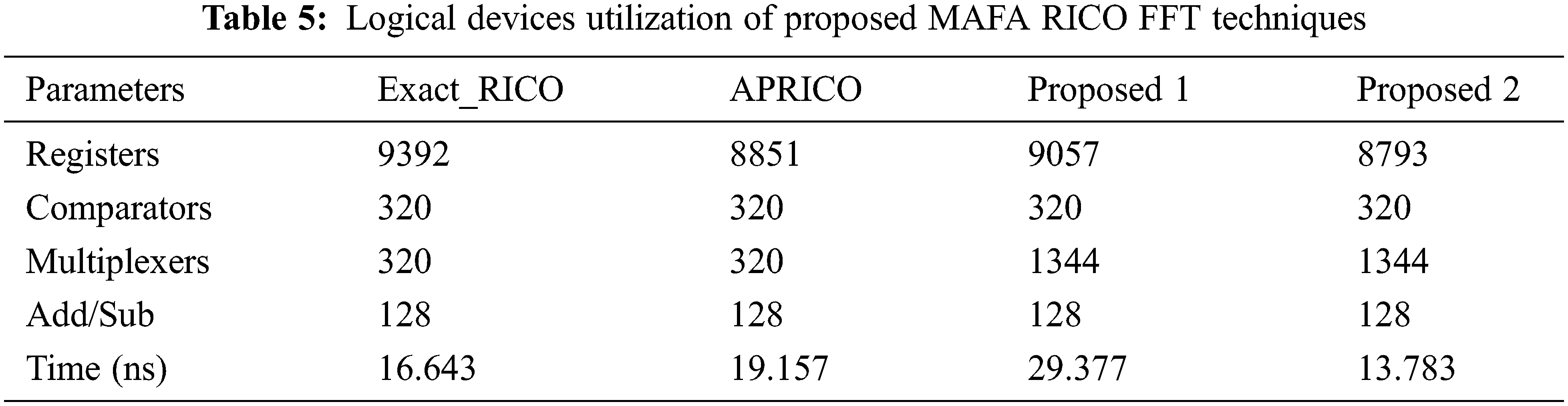
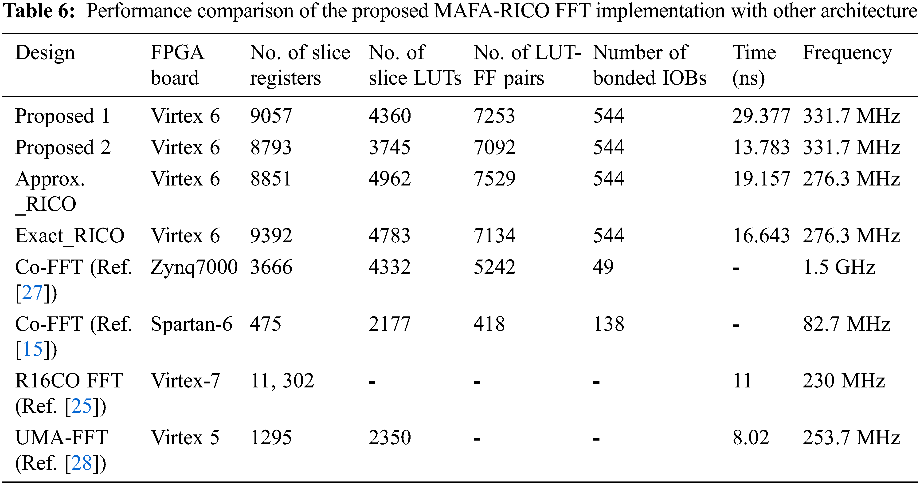
Tab. 6 compares our MAFA2-RICO FFT design to various approximation logic FFT architectures. The length of the FFT is considered when categorizing FFT architecture. Tab. 5 lists the resources and architecture required for the butterfly operation and the FFT method. The hardware needed to set up the data input and output FFT is not compared because it is application-specific. Various designs use FPGA specialized functional blocks like DSP and logic devices. For comparison, these blocks are reduced to slices. Built-in DSP block multiplier creates the butterfly processing unit. Built-in CORDIC algorithm for the butterfly processing unit. The butterfly processing unit uses an angle rotator with a multiplexer approximation full adder CORDIC algorithm, and the values are stored in slice registers and memory Lookup Tables (LUTs). Our method uses fewer slices than others. The recommended implementation’s alternative approximate FFT design yields a higher percentage improvement in slice utilization than the MAFA2-RICO CORDIC based FFT implementation. Tab. 6 shows that using FFT instead of the estimated RICO rotator-based technique saves resources by 19.37%.
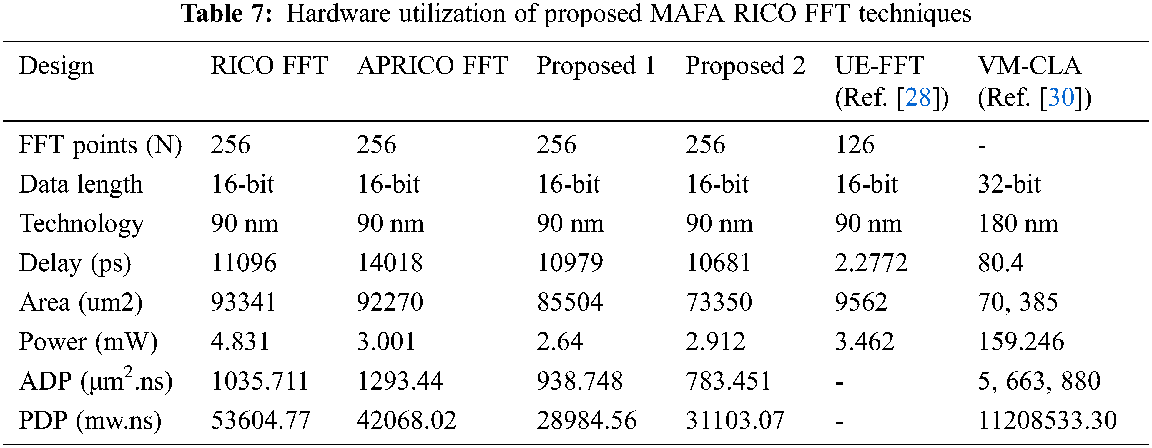
Tab. 7 compares the proposed method’s performance with other FFT approaches, such as RICO and APRICO. The suggested method’s performance metrics utilized to compare the proposed method’s results are the FFT size, area, power consumption, Power Delay Product (PDP), Area Delay Product (ADP), and execution time. The input for both the real and imaginary sections should be 16 bits in this situation. In addition, we developed a unique approximation logic adder for the 256-point FFT. Calculations using approximation logic result in considerable reductions in both minimum latency and FFT volume, as seen in Tab. 6. As a result, the power consumption of the FFT architecture was lowered. MAFA-RICO FFT has a lower ADP and PDP value than the regular RICO-FFT and various approximations of the RICO-FFT, as shown in Tab. 7. Traditional RICO, APRICO, MAFA1-RICO, and MAFA2-RICO FFTs use more PDP than the MAFA2-RICO-based FFT described here, which uses 41.13% less PDP.
In this work introduces a baseband UFMC modulator with a hardware-efficient reconfigurable architecture. The proposed architecture contains a variety of pulse-shaping filters that may select depending on the desired FOM, and there are no substantial changes in hardware resources necessary to choose the number of subcarriers in each subband. The experimental baseband signal validates the computations. In addition, we evaluated and compared the error bound of the suggested design because of its reconfigurability, hardware efficiency, and reuse of several hardware components. The proposed reconfigurable design for the UFMC modulator is ideally suited for 5G systems. UFMC systems may benefit from greater operating frequency by using the proposed architecture’s data and process level pipelining. When we examined parameters such as PAPR, BER, Spectral Density, and Spectral Efficiency, we were able to assess the effectiveness of the modulation schemes. This reconfigurable architecture might be enhanced by applying the modulation methods to distinct wireless communication channels. We want to enhance our proposed design for high-speed reconfigurable multicarrier systems.
Funding Statement: The authors received no specific funding for this study.
Conflicts of Interest: The authors declare that they have no conflicts of interest to report regarding the present study.
References
1. A. A., Zaidi, R. Baldemair, V. Moles-Cases, N. He, K. Werner et al., “OFDM numerology design for 5G new radio to support IOT, EMBB, and MBSFN,” IEEE Communications Standards Magazine, vol. 2, no. 2, pp. 78–83, 2018. [Google Scholar]
2. S. Doğan, A. Tusha and H. Arslan, “Noma with index modulation for uplink URLLC through grant-free access,” IEEE Journal of Selected Topics in Signal Processing, vol. 13, no. 6, pp. 1249–1257, 2019. [Google Scholar]
3. A. Asgharzadeh and M. Maroufi, “Performance analysis of 5G for low latency transmission based on universal filtered multi-carrier technique and interleave division multiple access,” Engineering World, vol. 3, pp. 52–57, 2021. [Google Scholar]
4. K. Zerhouni, R. Elassali, F. Elbahhar, K. Elbaamrani and N. Idboufker, “On the cyclostationarity of universal filtered multi-carrier UFMC,” AEU-International Journal of Electronics and Communications, vol. 89, pp. 174–180, 2018. [Google Scholar]
5. R. Gerzaguet, N. Bartzoudis, L. G. Baltar, V. Berg, J. B. Dore et al., “The 5G candidate waveform race: A comparison of complexity and performance,” EURASIP Journal on Wireless Communications and Networking, vol. 1, pp. 1–14, 2017. [Google Scholar]
6. Z. Zhao, M. Schellmann, X. Gong, Q. Wang, R. Böhnke et al., “Pulse shaping design for OFDM systems,” EURASIP Journal on Wireless Communications and Networking, vol. 1, pp. 1–25, 2017. [Google Scholar]
7. Z. A. Sim, F. H. Juwono, R. Reine, Z. Zang and L. Gopal, “Performance of GFDM systems using quadratic programming pulse shaping filter design,” IEEE Access, vol. 8, pp. 37134–37146, 2020. [Google Scholar]
8. Y. Jiang and X. Li, “Broadband cancellation method in an adaptive co-site interference cancellation system,” International Journal of Electronics, vol. 1, pp. 1–21, 2021. [Google Scholar]
9. R. S. Yarrabothu and U. R. Nelakuditi, “Optimization of out-of-band emission using kaiser-bessel filter for ufmc in 5G cellular communications,” China Communications, vol. 16, no. 8, pp. 15–23, 2019. [Google Scholar]
10. V. Kumar, M. Mukherjee, J. Lloret, Z. Ren and M. Kumari, “A joint filter and spectrum shifting architecture for low complexity flexible UFMC in 5G,” IEEE Transactions on Wireless Communications, vol. 20, no. 10, pp. 6706–6714, 2021. [Google Scholar]
11. M. Alsabah, M. A. Naser, B. M. Mahmmod, S. H. Abdulhussain, M. R. Eissa et al., “6G wireless communications networks: A comprehensive survey,” IEEE Access, vol. 9, pp. 148191–148243, 2021. [Google Scholar]
12. S. Domouchtsidis, C. G. Tsinos, S. Chatzinotas and B. Ottersten, “Symbol-level precoding for low complexity transmitter architectures in large-scale antenna array systems,” IEEE Transactions on Wireless Communications, vol. 18, no. 2, pp. 852–863, 2018. [Google Scholar]
13. A. R. Jafri, J. Majid, L. Zhang, M. A. Imran and M. Najam-ul-Islam, “FPGA implementation of UFMC based baseband transmitter: Case study for LTE 10 MHz channelization,” Wireless Communications and Mobile Computing, vol. 2018, pp. 1–13, 2018. [Google Scholar]
14. C. S. Park, S. Kim, J. Wang and S. Park, “Design and implementation of a farrow-interpolator-based digital front-end in lte receivers for carrier aggregation,” Electronics, vol. 10, no. 3, pp. 231–242, 2021. [Google Scholar]
15. Y. R. Manjunatha, “FPGA based efficient n-point FFT architecture using cordic for advanced OFDM,” International Journal of Engineering Research and Technology, vol. 11, no. 1, pp. 11–27, 2018. [Google Scholar]
16. V. Sakthivel and E. Elias, “Low complexity reconfigurable channelizers using non-uniform filter banks,” Computers & Electrical Engineering, vol. 68, pp. 389–403, 2018. [Google Scholar]
17. J. Zhao, S. Dang and Z. Wang, “Full-duplex relay-assisted orthogonal frequency-division multiplexing with index modulation,” IEEE Systems Journal, vol. 13, no. 3, pp. 2320–2331, 2018. [Google Scholar]
18. M. Abid, F. Ali, A. Armghan, F. Alenezi, S. Khan et al., “Architecture optimization for filtered multicarrier waveforms in 5G,” Wireless Personal Communications, vol. 1, pp. 1–24, 2022. [Google Scholar]
19. Y. A. Jawhar, L. Audah, M. A. Taher, K. N. Ramli, N. S. M. Shah et al., “A review of partial transmit sequence for PAPR reduction in the OFDM systems,” IEEE Access, vol. 7, pp. 18021–18041, 2019. [Google Scholar]
20. Z. Liu, X. Hu, K. Han, S. Zhang, L. Sun et al., “Low-complexity papr reduction method for OFDM systems based on real-valued neural networks,” IEEE Wireless Communications Letters, vol. 9, no. 11, pp. 1840–1844, 2020. [Google Scholar]
21. B. Bharathi and K. Kardas Rambabu, “A doubly selective channel estimation and interference cancellation scheme in FBMC-OFDM systems,” Turkish Journal of Computer and Mathematics Education, vol. 10, no. 3, pp. 841–848, 2019. [Google Scholar]
22. I. Baig, U. Farooq, N. U. Hasan, M. Zghaibeh and V. Jeoti, “A multi-carrier waveform design for 5G and beyond communication systems,” Mathematics, vol. 8, no. 9, pp. 1466–1485, 2020. [Google Scholar]
23. G. Visalli, “A novel coordinate rotation digital computer method for energy and latency saving by trigonometric operations spatial locality principle,” Journal of Low Power Electronics, vol. 15, no. 4, pp. 338–350, 2019. [Google Scholar]
24. P. K. Godi, B. T. Krishna and P. Kotipalli, “Design optimisation of multiplier-free parallel pipelined FFT on field programmable gate array,” IET Circuits, Devices & Systems, vol. 14, no. 7, pp. 995–1000, 2020. [Google Scholar]
25. A. Changela, Z. Mazad and D. Verma, “Mixed-radix, virtually scaling-free cordic algorithm based rotator for DSP applications,” Integration, vol. 78, pp. 70–83, 2021. [Google Scholar]
26. L. Hao, T. Chen and J. Yu, “Research on the application of cordic algorithm in the field of space-borne on-board signal processing,” Procedia Computer Science, vol. 183, pp. 361–371, 2021. [Google Scholar]
27. A. Banerjee and A. S. Dhar, “A novel paradigm of cordic-based FFT architecture framed on the optimality of high-radix computation,” Circuits, Systems, and Signal Processing, vol. 40, no. 1, pp. 311–334, 2021. [Google Scholar]
28. S. M. Noor, E. John and M. Panday, “Design and implementation of an ultralow-energy FFT ASIC for processing ecg in cardiac pacemakers,” IEEE Transactions on Very Large Scale Integration (VLSI) Systems, vol. 27, no. 4, pp. 983–987, 2018. [Google Scholar]
29. P. K. Meher and S. Y. Park, “Design of cascaded cordic based on precise analysis of critical path,” Electronics, vol. 8, no. 4, pp. 382–406, 2019. [Google Scholar]
30. R. Turaka, “Low power VLSI implementation of real fast Fourier transform with DRAM-VM-CLA,” Microprocessors and Microsystems, vol. 69, pp. 92–100, 2019. [Google Scholar]
31. R. Jothin and C. Vasanthanayaki, “High speed energy efficient static segment adder for approximate computing applications,” Journal of Electronic Testing, vol. 33, no. 1, pp. 125–132, 2017. [Google Scholar]
32. L. B. Soares, M. M. A. da Rosa, C. M. Diniz, E. A. C. da Costa and S. Bampi, “Design methodology to explore hybrid approximate adders for energy-efficient image and video processing accelerators,” IEEE Transactions on Circuits and Systems I: Regular Papers, vol. 66, no. 6, pp. 2137–2150, 2019. [Google Scholar]
33. R. Jothin and C. Vasanthanayaki, “High performance error tolerant adders for image processing applications,” IETE Journal of Research, vol. 67, no. 2, pp. 205–216, 2021. [Google Scholar]
34. H. Jiang, F. J. H. Santiago, H. Mo, L. Liu and J. Han, “Approximate arithmetic circuits: A survey, characterization, and recent applications,” IEEE Proceedings, vol. 108, no. 12, pp. 2108–2135, 2020. [Google Scholar]
35. N. K. Nawandar, B. Garg and G. K. Sharma, “Rico: A low power repetitive iteration cordic for DSP applications in portable devices,” Journal of Systems Architecture, vol. 70, pp. 82–92, 2016. [Google Scholar]
36. C. Thiruvengadam, M. Palanivelan, K. S. Kumar and T. Jayasankar, “Low power approximate adder based repetitive iteration cord (LP-ARICO) algorithm for high-speed applications,” Microprocessors and Microsystems, vol. 78, pp. 103260–103284, 2020. [Google Scholar]
Cite This Article
 Copyright © 2023 The Author(s). Published by Tech Science Press.
This work is licensed under a Creative Commons Attribution 4.0 International License , which permits unrestricted use, distribution, and reproduction in any medium, provided the original work is properly cited.
 Downloads
 Citation Tools