
 Submit a Paper
 Propose a Special lssue
 Open Access
ARTICLE
Design of a Novel Signed Binary Subtractor Using Quantum Gates
1 ICFAI University Tripura, Kamalghat, Agartala, West Tripura, India
2 JIS College of Engineering, Kalyani, Nadia, West Bengal, 741235, India
* Corresponding Author: Arindam Banerjee. Email:
Journal of Quantum Computing 2022, 4(3), 121-133. https://doi.org/10.32604/jqc.2022.034059
Received 05 July 2022; Accepted 07 April 2023; Issue published 03 July 2023
 View Full Text
 Download PDF
Abstract
In this paper, focus has been given to design and implement signed binary subtraction in quantum logic. Since the type of operand may be positive or negative, therefore a novel algorithm has been developed to detect the type of operand and as per the selection of the type of operands, separate design techniques have been developed to make the circuit compact and work very efficiently. Two separate methods have been shown in the paper to perform the signed subtraction. The results show promising for the second method in respect of ancillary input count and garbage output count but at the cost of quantum cost.Keywords
From decades ago, computer system works in binary arithmetic. The binary arithmetic, in the computing system, has been implemented using standard CMOS, Pass Transistor and Bi-CMOS technologies. In case of standard CMOS based implementation, speed improvement can not be achieved. After that FinFET has been introduced [1] for faster operation and it provides better sub-threshold swing. FinFET also provides better gain for the amplifiers. But in VLSI technology, the optimization of speed and power is a major challenge because to improve speed, power consumption must be increased. Therefore, some alternate technology to solve this issue has been thought of by the scientists. Reversible logic is considered to be a good solution to this issue because both speed and power consumption can be optimized in reversible logic system [2–5].
In [2], Landauer has explained the heat generation in computational process. In [3–5], Bennett has described the logical process of reversibility. In the year 1980, Toffoli [6] has proposed reversible gates for computation using Boolean logic. In the year 1981, Fredkin et al. [7] described the conservative logic in the reversible system. In 1985, Peres [8] has introduced a new reversible gate to synthesize Boolean functions. After few years, Deutsch [9], in 1985, has described the basic principles of quantum theory. In the year 2000, different quantum computing algorithms have been described by Nielsen et al. [10]. After that, several synthesis techniques for implementing Boolean functions in reversible logic have been reported in [11–18]. In [19], Moraga has described the use of double gates in reversible logic. The works in [12–14] show the arithmetic circuits implementation. In [12], a quantum ripple carry adder design has been reported. In [13–15], Thapliyal have proposed binary subtraction methods. But those methods are for unsigned binary number system.
In this paper, we propose another subtraction technique but the subtraction technique is for signed number system. The technique is new to the best of the knowledge of the authors and thus beyond the scope of comparison with other reported works.
2 Brief Overview of Basic Quantum Gates used for Arithmetic Operations
Basic quantum gates are associated with qubit operation. As defined in [9], Qubit is basically quantum state which is analogous to bit in binary number system. In binary number system, bit has two values logic 0 and logic 1 but in qubit, specific value may not be assigned since quantum states are probabilistic. Qubit can be written as
Fig. 1 shows the basic quantum gates. The solid circle notation indicates control input and the circled plus notation indicates the target input. The first gate is NOT or Feynman gate. It has the characteristics matrix
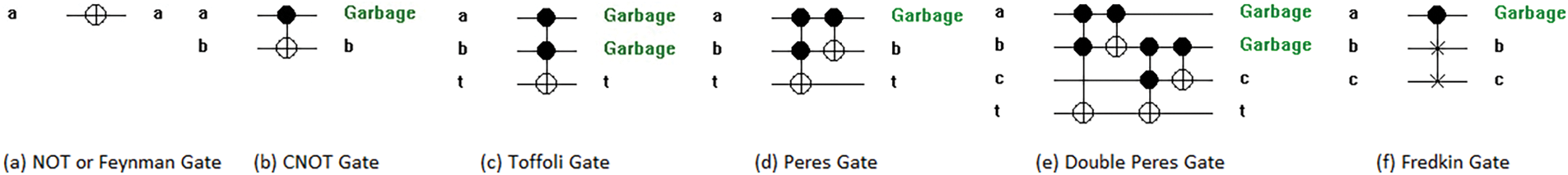
Figure 1: Basic quantum gates
Ancillary Input: It is defined as the extra constant input other than the primary inputs to evaluate the logic function.
Garbage Output: It is defined as the unused output other than the primary outputs to maintain logical reversibility. Garbage outputs are redundant outputs but they must be generated. If
Quantum Cost: It is the estimation of computational complexity of the circuit. It is defined as the number of quantum gates involved in the circuit implementation.
Fig. 2 shows a quantum circuit which represents logical OR operation. The first two gates combine to form a single Peres gate. As per the Boolean logic, the output at the third line is equal to

Figure 2: A quantum circuit representing OR operation

Figure 3: Decomposition of OR gate into unitary quantum gates
In Fig. 3, basically single Peres gate has been decomposed into unitary quantum gates based on the technique shown in [8]. Here few new quantum gates have been used V and V+ gates. V and V+ gates are represented as follows.
where
Lemma-1:
Proof: Since,
Similarly, Since,
Similar proof can be done for controlled V and V+ gates i.e.,
Lemma-2: One V or V+ gate and one NOT gate can be combined to generate a single quantum gate
Proof: We know that
Similarly,
Therefore there are 4 unitary gates and so the quantum cost is 4.
3 Mathematical Description of Signed Subtraction
Consider numbers A and B with extra sign bits (SignA and SignB). A and B can be represented as follows.
Similarly, (−A) and (−B) can be represented in 2’s complement form as follows.
The following table (Table 1) shows the subtraction operation with sign bits. Here SignA and SignB are the sign bits of the operand A and B.

4 Reversible Circuit Implementation for Signed Binary Subtraction
The signed subtraction technique shown in Table 1 has been verified using VHDL programming. The detailed code is shown in Fig. 4 and the verified output is shown in Fig. 5. The first two lines of the code are basically library declaration. Next part is the entity declaration which declares the input and the output signals. In the architecture part, there are two processes as shown in Fig. 4; one for addition or subtraction based on the signals (SignA and SignB); and the second for the 2’s complement operation based on the sign signals (SignA and SignB). In the first process of the code shown in Fig. 4, addition or subtraction has been performed based on the signs of the two operands (SignA and SignB). In the second process, the 2’s complement operation has been performed. It is a mixed style of the VHDL code because both dataflow and behavioral approaches have been used. For addition or 2’s complement operation, Boolean expressions, for half and full adder, have been used. As shown in Table 1, the 2’s complement operation has been performed based on the signal (SignA). Though the circuit has been implemented using reversible logic still VHDL implementation has been shown here to confirm the correctness of the procedure so that accurate circuit can be implemented in reversible logic.

Figure 4: Detailed VHDL code for binary subtraction (for 4 bit)

Figure 5: Waveform using Modelsim simulator for verification of the binary subtraction algorithm (for 4 bits)
The implementation scheme has two major parts: (i) addition or subtraction part and (ii) 2’s complement part. The first part (addition or subtraction) has been implemented using two types of addition methods. Figs. 6 and 7 show the two methods. Both the methods are generic and can be extended for any bit length. Like Fig. 5, “signa” and “signb” are the two signals which indicate the sign bits for the two operands as shown in Figs. 6 and 7. The outputs “Dif0” to “Dif3” are the results (here 4 bit operation has been shown). The signal “Sign” is the sign bit for the output. For the reversible circuit implementation, shown in Fig. 6, double Peres gates have been used for addition. For the circuit, shown in Fig. 7, the addition technique, as shown in [12], has been used.

Figure 6: Reversible circuit for signed binary subtraction (4 bit) (First Method)

Figure 7: Reversible circuit for signed binary subtraction (4 bit) (Second Method)
Ancillary Input Count:
First Method: Using Fig. 6, a generalized circuit for n-bit subtraction can be designed. The first part of the circuit is the addition or subtraction part. For n-bit operation, n number of ancillary inputs is required for addition or subtraction. The second part is for 2’s complement operation. It also requires n number of ancillary inputs. Therefore total
Second Method: In the second method, the first part (addition or subtraction) is replaced by a new adder circuit proposed in [12]. The adder circuit drastically reduces the number of ancillary inputs. Only 1 ancillary input is required for the addition. Therefore total
Garbage Output Count:
First Method: Number of ancillary inputs is
Second Method: In the second method,
Quantum Cost Count:
First Method: For arithmetic operation, here, single Peres and double Peres gates have been used. Decomposition of Peres gate and double Peres gate into quantum gates is shown in Figs. 8 and 9. The decomposition technique of double Peres gate, shown in Fig. 9, follows the technique in [19] proposed by Moraga. For single Peres gate, the quantum cost is 4 and for double Peres gate, the quantum cost is 6 as shown in Figs. 8 and 9. For the design of half adder, single Peres gates are used which can be decomposed into quantum gates as shown in Fig. 8. For the full adder circuit implementation, double Peres gates are used as shown in Fig. 9. At first, the double Peres gate can be decomposed into quantum gates as shown in the upper part of Fig. 9. The circuit can be further optimized by eliminating redundant gates as shown in the lower part of Fig. 9. In Fig. 9, the combination of one V gate and one V+ gate, indicated by a box, is an identity gate and thus the combination is a redundant gate. This can be proved as given below.

Figure 8: Decomposition of Peres gate into quantum gates

Figure 9: Decomposition of double Peres gate into quantum gates
Lemma-3: One V gate and one V+ gate can be combined to generate an identity gate
Proof: We know that
Similarly, it can be proved that,
In the circuit shown in Fig. 6, in general
Second Method: For the second method, the adder proposed in [12] has been used. The single bit adder circuit can be decomposed into several quantum gates shown in Fig. 10. The two circuits indicated in square boxes in Fig. 10 are two quantum gates because they are unitary matrices. It can be proved in the following Lemma.

Figure 10: Decomposition of the new adder circuit into quantum gates
Lemma-4: The combination of one NOT and one V gate forms a unitary gate
Proof: As we know that
One single bit adder circuit has the quantum cost 13 as counted from Fig. 9. Thus for n-bit operation, the total quantum cost is
As shown in Table 2, for the second method, the ancillary input count is reduced by almost

A novel signed subtraction technique was shown in the paper. The technique is unique in the sense it used four types of operands (positive–positive, positive–negative, negative–positive and negative–negative) and for the four types of operands, the algorithm worked efficiently. The algorithm was verified using HDL programming and then it was implemented in reversible logic. Here two different addition techniques were shown for the subtraction. Finally the reversible circuit was implemented using the quantum gates. It could be concluded that the second method was better in respect of fabrication cost whereas the first method was better in respect of the computational complexity.
7 Future Scope of the Research
In future, the work can be extended to the design optimization of other arithmetic circuits like, signed multiplier, squarer, exponential computation etc. using quantum gates.
Funding Statement: The authors received no specific funding for this study.
Conflicts of Interest: The authors declare that they have no conflicts of interest to report regarding the present study.
References
1. A. Marshal, Circuit Design Using a FinFET Process. Dallas: Texas Instruments Incorporated, 2006. [Online]. Available at: https://ewh.ieee.org/soc/cas/dallas/documents/Sem-012506-Andrew_FinFET.pdf [Google Scholar]
2. R. Landauer, “Irreversibility and heat generation in the computational process,” IBM Journal of Research and Development, vol. 5, no. 3, pp. 183–191, 1961. [Google Scholar]
3. C. H. Bennett, “Logical reversibility of computation,” IBM Journal of Research and Development, vol. 17, no. 6, pp. 525–532, 1973. [Google Scholar]
4. C. H. Bennett, “The thermodynamics of computation—A review,” IBM Journal of Research and Development, vol. 21, pp. 905–940, 1981. [Google Scholar]
5. C. H. Bennett, “Notes on the history of reversible computation,” IBM Journal of Research and Development, vol. 32, no. 1, pp. 16–23, 1998. [Google Scholar]
6. T. Toffoli, Reversible Computing. Cambridge, New York, USA: Technical Memo MIT/LCS/TM-151, MIT Lab for Computer Science, pp. 1–37, 1980. [Google Scholar]
7. E. Fredkin and T. Toffoli, “Conservative logic,” International Journal of Theoretical Physics, vol. 21, pp. 219–253, 1981. [Google Scholar]
8. A. Peres, “Reversible logic and quantum computers,” Physical Review A, vol. 32, pp. 3266–3276, 1985. [Google Scholar]
9. D. Deutsch, “Quantum theory, the Church-Turing principle and the universal quantum computer,” Proceedings of the Royal Society of London, vol. A400, pp. 97–117, 1985. [Google Scholar]
10. M. A. Nielsen and I. L. Chuang, Quantum Computation and Quantum Information. Cambridge, New York, USA: Cambridge University Press, 2000. [Google Scholar]
11. R. Wille and R. Drechsler, Towards a Design Flow for Reversible Logic. Germany: Springer, 2010. (https://doi.org/10.1007/978-90-481-9579-4) [Google Scholar] [CrossRef]
12. S. Cuccaro, T. Draper, D. Moulton and S. Kutin, “A new quantum ripple-carry addition circuit,” in Proc. of the 8th Workshop on Quantum Information Processing, Cambridge, pp. 1–9, 2005. [Google Scholar]
13. H. Thapliyal and N. Ranganathan, “Design of efficient reversible binary subtractors based on a new reversible gate,” in IEEE Proc. of the Computer Society Annual Symp. on VLSI, Tampa, FL, USA, pp. 229–234, 2009. [Google Scholar]
14. H. Thapliyal and N. Ranganathan, “A new design of the reversible subtractor circuit,” in Proc. of IEEE Int. Conf. on Nanotechnology, Portland, pp. 1430–1435, 2011. [Google Scholar]
15. H. Thapliyal, “Mapping of subtractor and adder-subtractor circuits on reversible quantum gates,” in Transactions on Computational Science XXVII, vol. 9570. Berlin, Heidelberg: LNCS, Springer, pp. 10–34, 2016. [Google Scholar]
16. R. Wille, O. Keszocze, L. Othmer, M. K. Thomsen and R. Drechsler, “Generating and checking control logic in the HDL-based design of reversible circuits,” in Int. Symp. on Embedded Computing and System Design, Patna, India, pp. 7–12, 2016. [Google Scholar]
17. M. Soeken, R. Wille, O. Keszöcze, D. M. Miller and R. Drechsler, “Embedding of large boolean functions for reversible logic,” ACM Journal on Emerging Technologies in Computing System, vol. 12, no. 4, pp. 41(1)–41(262016. [Google Scholar]
18. A. Zulehner and R. Wille, “Improving synthesis of reversible circuits: Exploiting redundancies in paths and nodes of QMDDs,” in Reversible Computation, Kolkata, India, pp. 232–247, 2017. [Google Scholar]
19. C. Moraga and F. Z. Hadjam, “On double gates for reversible computing circuits,” in Proc. Int. Workshop on Boolean Problems, Freiberg University of Mining and Technology, Germany, 2012. [Google Scholar]
Cite This Article
 Copyright © 2022 The Author(s). Published by Tech Science Press.
This work is licensed under a Creative Commons Attribution 4.0 International License , which permits unrestricted use, distribution, and reproduction in any medium, provided the original work is properly cited.
 Downloads
 Citation Tools