
 Submit a Paper
 Propose a Special lssue
 Open Access
ARTICLE

Nitrogen-Doped Amorphous Carbon Homojunction from Palmyra Sugar as a Renewable Solar Cell
1 Department of Electronic Engineering, Faculty of Engineering, Universitas Muhammadiyah Malang, Kota Malang, Indonesia
2 Advanced Materials Research Group, Department of Physics, Faculty of Science and Data Analytics, Institut Teknologi Sepuluh Nopember, Surabaya, Indonesia
3 Department of Electronic Engineering, Faculty of Industrials Engineering, Institut Teknologi National Malang, Kota Malang, Indonesia
* Corresponding Authors: Budhi Priyanto. Email: ; Darminto. Email:
Journal of Renewable Materials 2024, 12(1), 57-69. https://doi.org/10.32604/jrm.2023.028619
Received 29 December 2022; Accepted 09 June 2023; Issue published 23 January 2024
 View Full Text
 Download PDF
Abstract
An a-C/a-C:N junction, which used palmyra sugar as the carbon source and ammonium hydroxide (NH4OH) as the dopant source, was successfully deposited on the ITO glass substrate using the nano-spraying method. The current-voltage relationship of the junction was found to be a Schottky-like contact, and therefore the junction shows the characteristic rectifiers. This means the a-C and a-C:N are semiconductors with different types of conduction. Moreover, the samples showed an increase in current and voltage value when exposed to visible light (bright state) compared to the dark condition, thereby, indicating the creation of electron-hole pairs during the exposure. It was also discovered that the relationship between current and voltage for the a-C/a-C:N junction sample formed a curve that satisfies the rule of the photovoltaic effect when exposed to visible light from a light bulb. The exposure of this sample to direct sunlight at AM 1.5 conditions produced a curve that meets the rules for the emergence of the photovoltaic effect with higher characteristics for the current-voltage relationship. Thus, the a-C/a-C:N junction sample is a solar cell successfully fabricated using a sample method and has a maximum efficiency of 0.0013%.Graphic Abstract

Keywords
Carbon is one of the elements in group IV besides silicon. Although in the same group, it differs from silicon in hybridization. Silicon has a single hybridization, namely sp3, while carbon has three hybridizations, namely sp3, sp2 and sp. carbon with 100% sp3 hybridization is known as diamond like carbon (DLC) and acts as an insulator. Carbon with 100% sp2 hybridization is known as graphite and is an excellent conductor. Carbon with mixed sp3 and sp2 hybridization is known as amorphous carbon. The percentage of carbon hybridization is strongly influenced by its hydrogen content, the deposition parameter and the raw materials of the carbon source. In this various hybridization, carbon compounds may have various energy gaps in the range of 0 to 6 eV [1,2].
Thin Carbon films are generally deposited using the Chemical Vapor Deposition (CVD) method with hydrocarbon compounds as the precursors, such as ethanol [3], methane gas [4–8], di-iso-propyl-ether ((i-C3H7)2O) [9], acetylene [10]. The percentage of sp3, sp2 and sp hybridization is strongly influenced by the carbon source. Methane gas sources provide a higher percentage of sp3 than acetylene. The percentage of sp2 is higher when an acetylene source is used. Diamond like carbon (DLC) deposited using a methane gas source is more insulating than that from an acetylene source [11].
Amorphous carbon thin films have been successfully prepared using the CVD method from biomass sources. These films sourced from palm oil have been successfully deposited on glass and p-type silicon [12]. Nitrogen-doped amorphous carbon thin films with ethanol as the source and nitrogen gas as the doping source have been successfully deposited on a p-type silicon substrate [13]. One of the deposition methods besides CVD to prepare amorphous carbon thin films is the spin coating method. Has been successfully deposited using the spin coating method of amorphous carbon thin film with biomass sources (coconut sugar, palmyra sugar, palm sugar and brown sugar), which are deposited on ITO glass substrate. The percentage value of sp2 hybridization is above 60%, and the value can be adjusted by adjusting the heating temperature of the carbon source. The electrical conductivity values of the amorphous carbon thin films formed are within the range of the electrical conductivity values of semiconductor materials [14–16].
Carbon is a material with great potential for the development of photovoltaic cells. Amorphous carbon absorbs much higher sunlight of sunlight than amorphous silicon at the same thickness [17]. Its high absorption of sunlight provides the potential for carbon applications such as an anti-reflective coating in silicon solar cells [18,19]. Polymeric-like carbon (PLC) and DLC deposited using CVD have been applied as anti-reflective coatings for crystalline silicon solar cells [20]. The extraordinary electronic properties of carbon make it an important component in the development of solar cells. Because of its high electrical conductivity, carbon is used as a back contact in perovskite solar cells [21]. Due to the high electrical conductivity of carbon, it is used as an electrode in perovskite solar cells [22].
Carbon-based solar cells that have been developed previously are generally a heterojunction between carbon and silicon. The carbon source comes from hydrocarbon compounds, and the deposition process uses the (CVD) method. Carbon-based solar cells have been successfully made using SWCVD with an acetylene source and trimethyl boron as a doping source for a p-type layer. The samples were deposited on an n-type silicon substrate in two p-C/n-Si and p-C/i-C/n-Si configurations [23]. Using rf-PECVD, a solar cell with the p-PAC/i-a-Si:H/n-Si:H configurations has been successfully fabricated [24]. Using AACVD, carbon-based solar cells have been successfully made with camphor oil as a source. Solar cell samples were made in Au/p-C/n-Si/Au configuration [25]. Using AACVD with camphor oil sources, heterojunction solar cells with Au/n-C:N/p-Si/Au and Au/a-C/p-Si/Au configuration have been successfully fabricated. Nitrogen gas is used as a doping source. A Solar cell sample with Au/a-C/p-Si/Au configuration when measured using a PV simulator at AM 1.5 condition obtained an efficiency of 0.000048% [26]. Carbon nanomaterials were integrated with silicon solar cells to form a CNT-Si configuration [27]. Carbon-derived homojunction solar cells with a-C/fullerene(C60) configuration [28,29]. So far, carbon-based solar cells have been dominated by a carbon-silicon heterojunction. Amorphous carbon homojunction solar cells have not yet been developed by previous researchers. The main source of doping in the development of solar cells are gaseous doping sources [12,13,23,25,26], and liquid doping sources have never been used. The main source of carbon as active material is dominated by hydrocarbon compounds, and the use of carbon derived from agricultural products (biomass) has not been significantly developed. The deposition method is dominated by CVD and other deposition methods have not been developed for the carbon-based solar cells.
In this research, amorphous carbon thin film deposition has been carried out with a new method that has not been carried out by previous researchers, namely the nano-spraying method. These thin films of amorphous carbon cover boron-doped amorphous carbon and nitrogen-doped amorphous carbon on ITO glass substrates using the nano-spraying method have been successfully prepared with palmyra sugar as a carbon source. The carbon thin film that has been successfully deposited has a smooth, uniform, thin surface (one hundred nanometer), and has good transmission of visible light and infrared.
This paper reports the results of the research on the development of amorphous carbon-based solar cells. The solar cell sample is an amorphous carbon homojunction, which has never been done by previous researchers. The deposition method uses nano-spraying, which has never been done in the development of solar cell technology. The carbon source uses palmyra sugar, which is an agricultural product, available all year round and is renewable, abundant and very cheap. The doping process uses a liquid ammonium hydroxide (NH4OH) source. The results of measuring the electrical conductivity of each layer using a four-point probe, the optical energy gap using UV-Vis spectroscopy, and PES testing to determine the occurrence of the doping process included. The results of current and voltage measurements indicate that the sample junction function as a rectifier and as a photovoltaic cell.
Palmyra sap contains an element C of 61.9%, O of 35.84%, Cl of 0.68%, Na of 0.81%, K of 0.41%, P of 0.18%, S of 0.06% and Si of 0.01%, which is very good for use as a natural carbon source. The sap is produced from palmyra trees (Fig. 1a) by pruning the flowers that have not yet bloomed. The water that oozes out of the flower stalk is the sap. The sap from the stalk is collected in a vessel. When the volume of the sap has reached a sufficient amount, it is processed to become dilute sugar. The sap that is sufficient must be immediately processed to diluted sugar so that is not decay. It is heated in open air and stirred so that the evaporation occurs as expected. When the water content is reduced as expected, the cooling process is carried out until it becomes diluted sugar. This process is carried out by farmers in the Palmyra plantation. The yellowish diluted sugar produced from the Palmyra plantation is heated using a hotplate at a temperature of 100°C and stirred with a magnetic stirrer within 120 min to reduce water content. Cooling is done to get dark brown thick sugar (Fig. 1b). Further heating is carried out using a furnace at a temperature of 250°C for 150 min, and cooling is carried out in the furnace. This process produces a very light, shiny black charcoal. The charcoal is washed with distilled water and filtered using paper to remove the potassium chloride (KCl) content. The dry charcoal is crushed until very fine powdered charcoal is obtained.
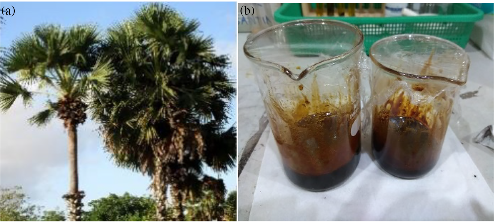
Figure 1: (a) Palmyra trees, (b) Thick palmyra sugar
Meanwhile, the a-C:N powder is prepared by mixing a-C powder with ammonium hydroxide (NH4OH, Merck 25%) at an a-C with an NH4OH mole ratio of 1:0.066. The mixture is heated using a hotplate at 150°C and stirred with a magnetic stirrer at 200 rpm for 120 min. Moreover, the a-C solution is prepared by mixing 2 g of a-C powder with 10 ml of dimethyl sulfoxide (DMSO, Merck 99.9%), which is used as a solvent in addition to 10 ml of distilled water. The solution is heated at 100°C, stirred with a magnetic stirrer at 1500 rpm for 60 min, and exfoliated using ultrasonic for 30 min. It is rotated at 3500 rpm for 30 min using a centrifuge of 80-2 to separate large carbons. It is also important to note that the a-C:N solution is prepared using the same process used for the a-C solution.
To obtain the characteristic of each layer, thin film deposition of a-C and a-C:N was carried out on a 2 × 2 cm2 ITO glass substrate. Furthermore, the junction sample is deposited on a 2 × 1 cm2 ITO glass substrate using a nano-sprayer (30 ml USB handy nano mist sprayer Fig. 2a) while the a-C/a-C:N junction samples are deposited on size of 1 × 1 cm2 as illustrated in Fig. 2b. The thin film deposition process begins by inserting solution a-C and a-C:N into the solution container. Before the solution is deposited on the surface of the substrate, several steps occur. These stages are the process of atomization of the solution, flight of droplets to the surface of the substrate, contact of droplets with the surface of the substrate, dispersion and evaporation. The atomizer or nebulizer is intended to form very fine granules from the solution. These very fine granules are accelerated by applying pressure or a high-velocity flow of gas. The very finest of granules are pushed out through the outlet hole and fly to the surface of the substrate. This process occurs inside the nano-sprayer device and occurs shortly after the switch is turned on. The very fine grains directed towards the surface of the substrate form a lamellar layered precipitate. Only grains of the order one nanometer can exit the outlet hole. The grain size greatly determines the quality of the layer formed. The deposition process ends shortly after the switch is turned off. The evaporation process in the atmosphere and contamination from the surrounding environment is protected. This process is carried out within 3 days and a thin film is obtained on the ITO glass substrate. Each layer is deposited within 10 s and the distance between the substrate and solution outlet hole on the nano-sprayer is 5 cm. The sample of the a-C/a-C:N junction is carried out by first depositing the a-C/N on an ITO glass substrate. After the drying process is complete, the a-C layer is deposited on top as illustrated in Fig. 2b.
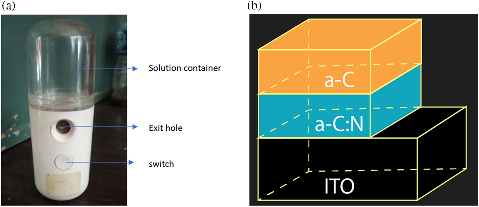
Figure 2: (a) Nano-sprayer, (b) Illustration of a sample on a glass ITO substrate
2.2 Characterization of Each Layer
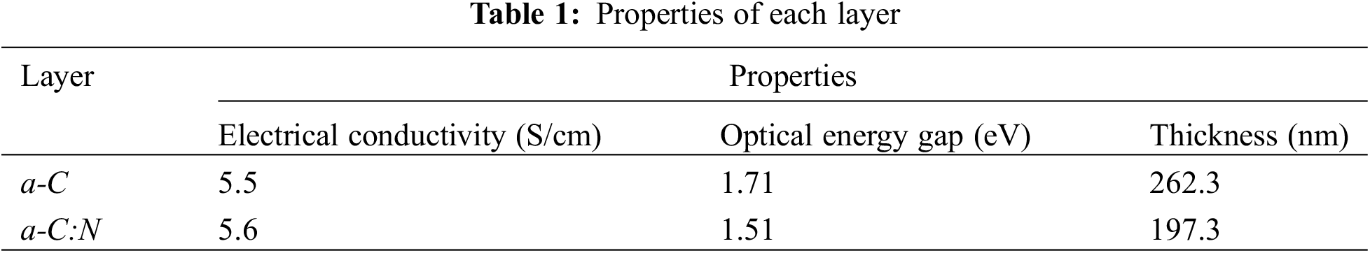
The electronic properties and the structure of each layer are important components that influence the characteristics of the junction sample. XRD (Philip X’ Pert MPD with Cu Kα radiation and diffraction angle in the range 10°–60°) analysis showed that a-C and a-C:N layers were in the amorphous phase. Moreover, the electronic and optical properties of the coating greatly affected the junction characteristics of the sample. It was also discovered that the sample could function as a solar cell when each layer has semiconductor electronic properties and an optical energy gap that allows the formation of electron-hole pairs in the visible light region. The electrical conductivity and optical energy gap of each layer obtained using the 4-point probe and UV-Vis spectroscopy (GENESIS 10 S with a wavelength in the range of 400–1000 nm) analyses are presented in Table 1. The current and voltage in each layer were discovered to have a linear relationship (ohmic contact).
The results of measuring the transmission properties of amorphous carbon (a-C) and nitrogen-doped amorphous carbon (a-C:N) thin film are shown in Fig. 3a. It can be seen that the transmission properties of light show an increasing value with increasing wavelength. The maximum transmittance value occurs at a wavelength of 900 nm with an energy ∼1.3 eV. This wavelength is the near-infrared region. So amorphous carbon and nitrogen-doped amorphous carbon film exhibit transparent properties in the region ∼1.3 eV, characterized by a transmittance value of around 100%. The value of the optical gap energy of a-C and a-C:N films can be calculated using the Tauc formula. The value is obtained by extrapolation as shown in Fig. 3b.
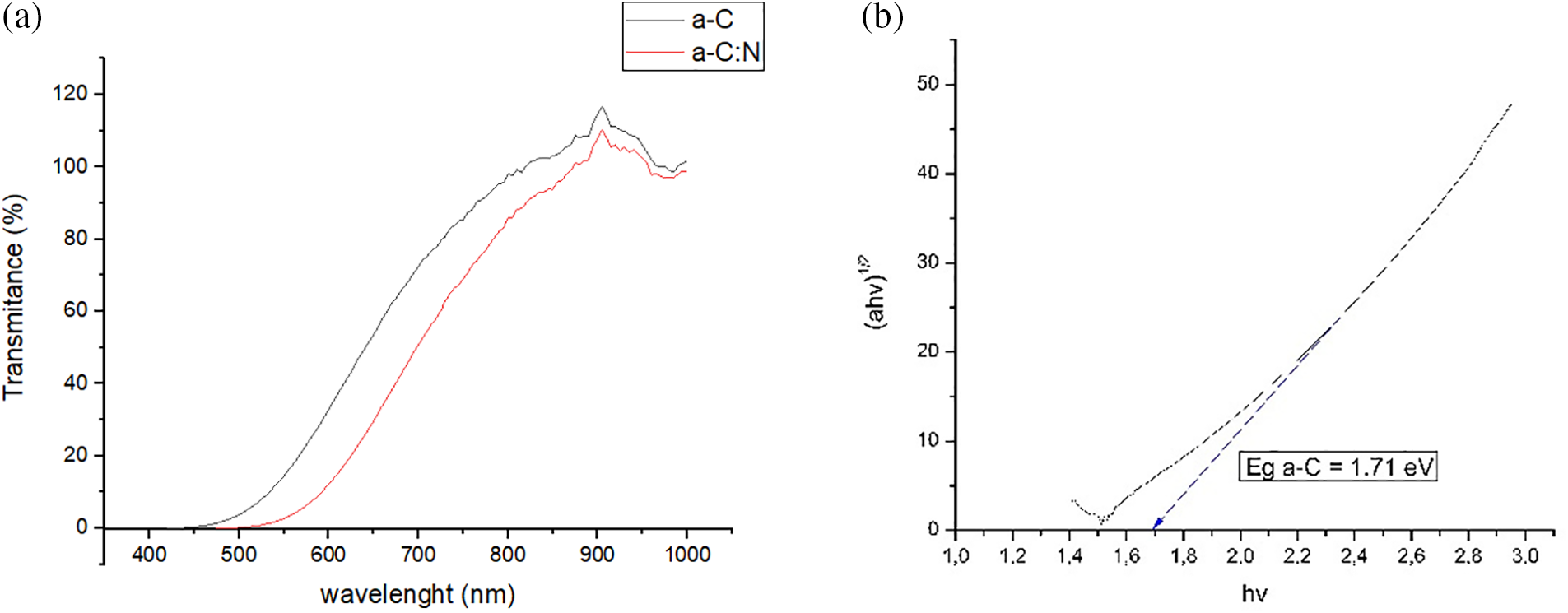
Figure 3: UV-Vis measurement results. (a) Transmittance a-C and a-C:N films. (b) Optical gap energy calculation using Tauc extrapolation
The surface morphology of each layer was determined through the Scanning Electron Microscope (SEM ZEISS EVO 10) while the structure was evaluated using the photoemission spectroscopy (Syn. PES at beam line 3.2a in the Synchrotron Light Research Institute/SLRI Thailand facility). Mode XPS under ultra-high vacuum (<1 × 10⁻⁵ Pa) and photon energy in the range 40 to 600 eV, and the results are presented in Fig. 4. The particles in a-C and a-C:N were observed to be in the order of hundreds of nanometers. The PES test was further reviewed on the C1s of a-C and a-C:N layers dominated by sp2 hybridization and C-N bonds, and the formation of C-N bonds indicated the possibility of doping and defect processes.
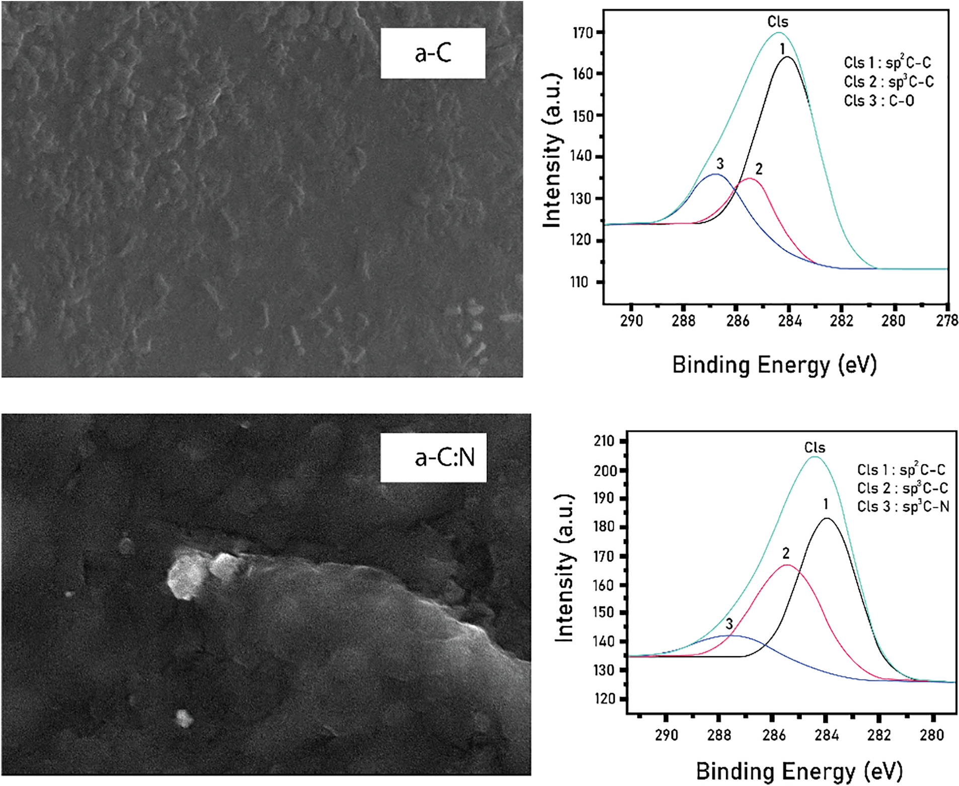
Figure 4: Morphology and structure of each layer
The results of the PES analysis conducted on the N1s spectra are shown in Fig. 5. It was discovered that the spectrum can be deconvoluted into three main components which include Pyridinic-N with 398.83 eV [reference 398.5 ± 0.1], Pyrrolic-N with 399.93 eV [reference 400.2 ± 0.1], and Graphitic-N with 400.893 eV [reference 401.2 ± 0.1]. It is also important to note that the C-N bond is a doping process that involves the replacement of a C atom by an N atom. In the graphitic-N, the C atoms were replaced by N atoms, and this caused doping while a defect was found in pyrrolic-N and pyridinic-N, which led to the absence of the doping process [30]. The formation of graphitic-N allowed the a-C:N to become an n-type semiconductor while the a-C layer has an intrinsic conduction type. Furthermore, the deconvolution of the N1s spectrum in the a-C:N layer produced 41.9% pyridinic-N, 39.6% pyrrolic-N, and 18.5% graphitic-N.
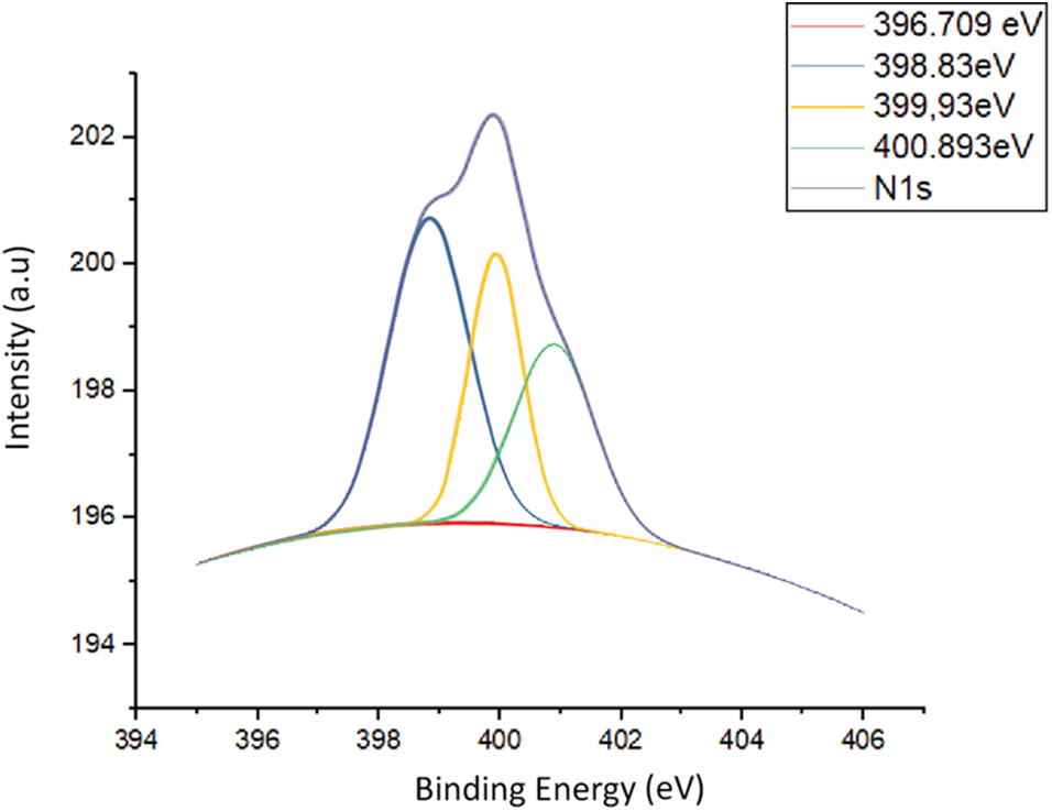
Figure 5: Deconvolution of N1s spectrum
A solar cell is a photodiode in principle, which means that the junction of two semiconductor materials having different types of conduction is required to comply with the basic rules of a diode required to function as a rectifier. The diode characteristics of the a-C/a-C:N junction sample were determined by measuring the current and voltage. The measurement results are presented in the graph in Fig. 6. It was discovered that the relationship between the two indicators meets the rules required or the sample to function as a rectifier. This strengthens the results of testing using PES which shows the occurrence of the doping process and a-C:N has a different conduction type than a-C. These results proved that a-C is intrinsic i while a-C:N is an n-type. The results of the current and voltage test provide evidence that rectifier diodes can be made from materials other than silicon. Carbon from biomass can be used as the active material for diodes with cheaper, easier and simpler manufacturing technology. The a-C/a-C:N junction is an i-n junction diode with a reverse bias current of 127.7 nA, a forward bias voltage of 3.3 mV, and a breakdown voltage of −3.95 mV.
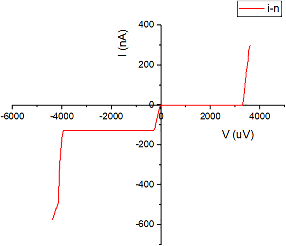
Figure 6: I-V curve of a-C/a-C:N junction
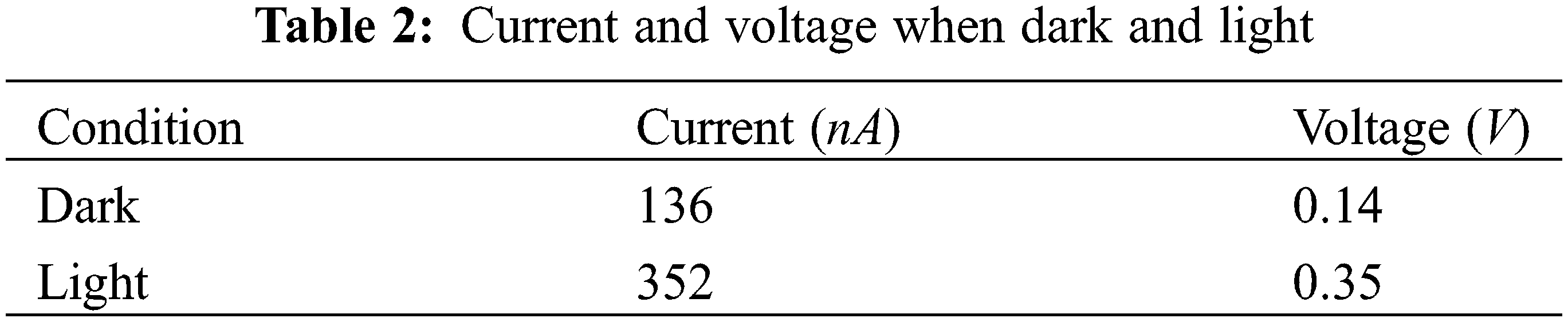
The diode function as a photodiode is characterized by the difference in current and voltage values when in dark conditions compared to bright conditions. The sample functioning as a photodiode is tested by comparing the current and voltage value in the sample when it is dark compared to the value when the sample is illuminated with 1660 lux light. The results of measuring the current and voltage values when dark and when it is illuminated with 1660 lux light are shown in Table 2. The results presented in Table 2 showed an increase in the value of current and voltage when the sample was exposed to light compared to the dark. This shows that the sample functions as a photodiode and has the potential to also function as a photovoltaic cell.
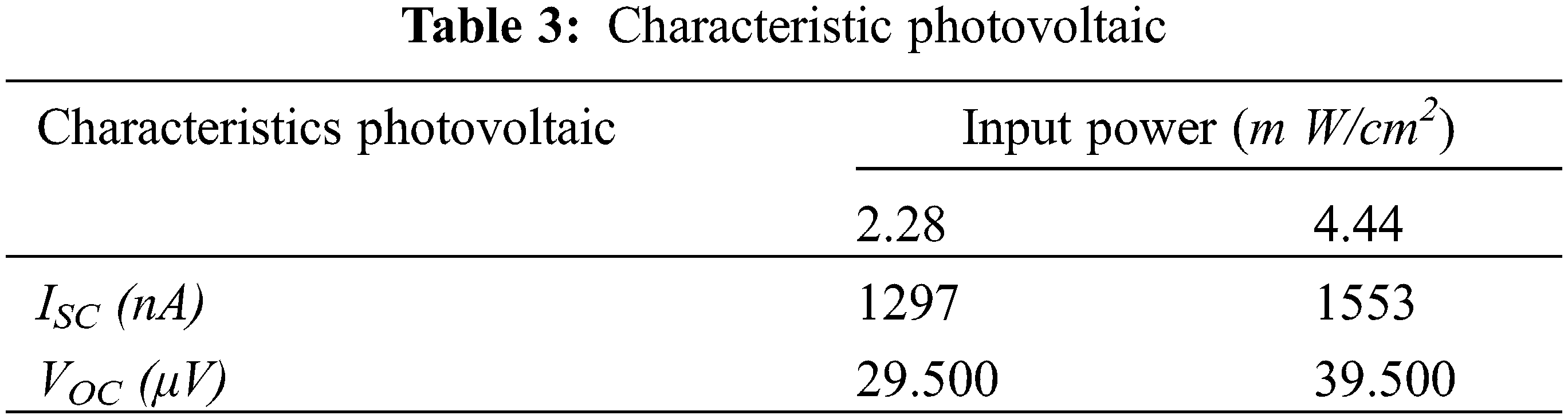
Whether the sample functions as a photovoltaic cell is found out by measuring the current and voltage values when the sample is exposed to visible light, current and voltage values were measured when the sample was exposed to visible light from lamps with an input power 2.28 and 4.44 m W/cm2, and exposure to direct sunlight at AM 1.5 condition. The relationship between current and voltage when the sample is exposed to visible light from the lamp is shown in Fig. 7. The curve in Fig. 7 shows that the relationship between current and voltage fulfills the rules for the occurrence of the photovoltaic effect. The characteristic values from photovoltaic cells when exposed to light from a lamp are shown in Table 3. Table 3 shows an increase in short circuit current (ISC) and open circuit voltage (VOC) with increasing emitted light power. The increase in ISC and VOC values does not seem to be directly proportional to the input power. This can be seen when the input power is increased two times; the increase in ISC and VOC values is not two times either.
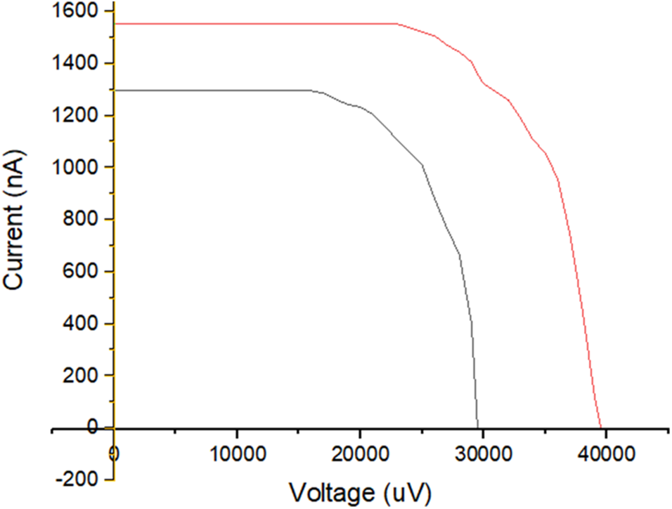
Figure 7: I-V curve on exposure to light
The sample was also exposed to direct sunlight at AM 1.5 (100 m W/cm2), and the relationship between the current and the generated voltage is presented in Fig. 8. It was discovered that the relationship also fulfills the requirement for the emergence of the photovoltaic effect.
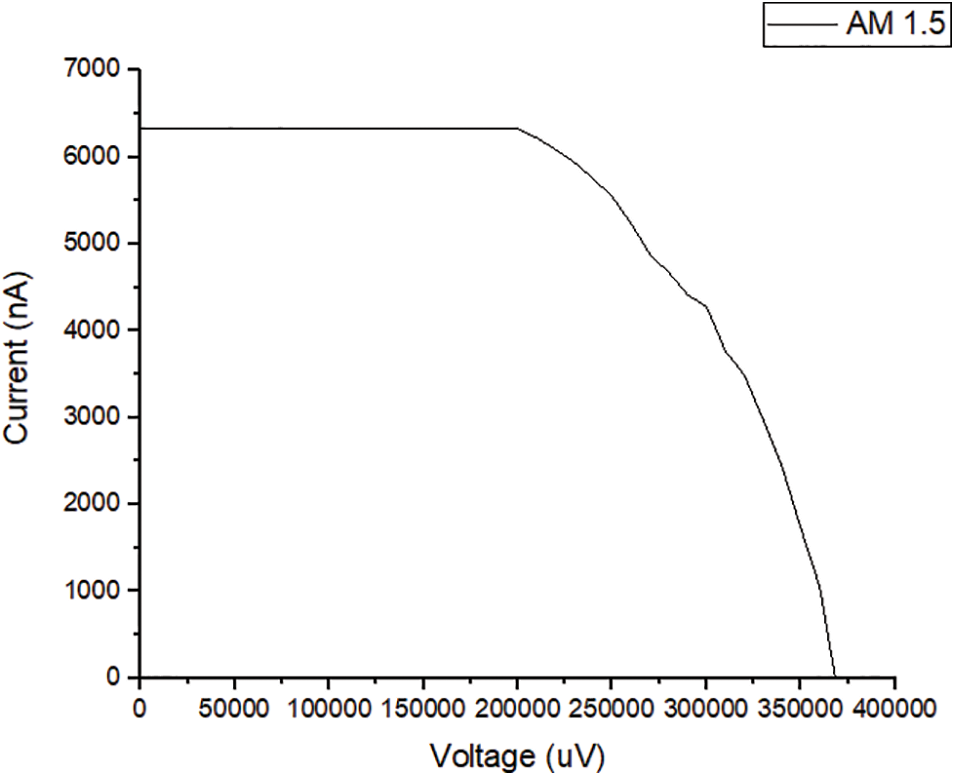
Figure 8: The curve of the relationship between current and voltage AM 1.5 conditions
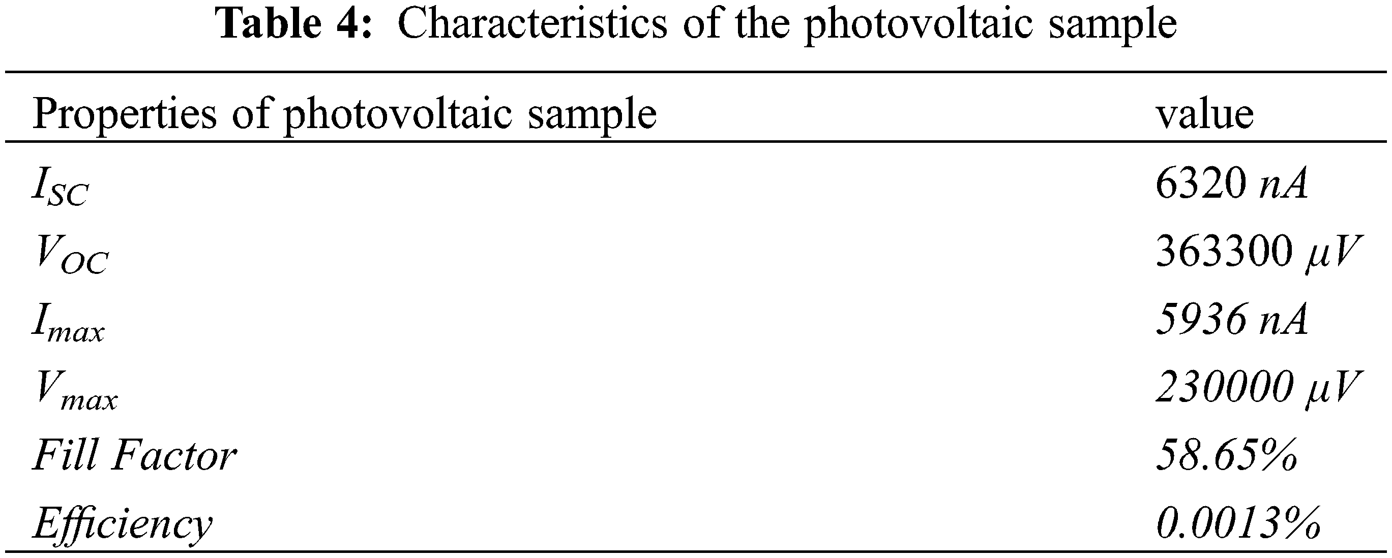
This proves that the junction sample is a photovoltaic cell because the electron in the valence band of the type i layer receives sufficient energy to be excited toward the conduction band when the sample is exposed to light to become a free electron and leave a hole in the valence band. This causes the type i layer to have an excess of holes. Meanwhile, light exposure in the n-type layer is able to excite an electron from the valency band to the conduction band to become a free electron and the n layer has excess electrons. The hole in the i layer is unable to diffuse to the n-type because it is blocked by the built-in electric field in the depletion layer while the electron passes through the depletion region toward the n-type layer. It is important to note that the electron flows toward the external resistance. However, the hole in the n-type breaks through the depletion region to the type-i region and flows into the external resistance. This means the holes and electrons flow into the external circuit as an electric current to create a potential difference across the external resistance. The current and voltage in this external circuit were found to be the benchmarks for the output power of the solar cell sample. This shows that the electron-hole pairs arose when exposed to light in the a-C/a-C:N junction sample, indicating its ability to function as a solar cell. The ability of the sample to function as a solar cell depends highly on the current flowing in the external circuit. It was discovered that the short circuit current (ISC) and open circuit voltage (VOC) increased when it was exposed to direct sunlight. The maximum current and voltage in the curve presented in Fig. 8 were used to calculate the photovoltaic characteristics of the junction sample, and the results obtained are listed in the following Table 4. The table shows that the sample functions as a solar cell with a maximum efficiency of 0.0013%. In Table 4, it can be seen that the ISC is still too small compared to VOC. There is a possibility of a recombination process immediately after the generation of an electron and a hole after the sample is exposed to light. The reason for the recombination is probably that the thickness of each layer of the spliced sample is not optimal. It is still too thin. The second probability is caused by a defect in the a-C:N layer, which is characterized by the formation of Pyridinic-N and pyrrolic-N compounds.
This research is initial research on the development of solar cells using a biomass source. The developed solar cell is an amorphous carbon homojunction that has not been developed by previous researchers. Previous development of carbon-based solar cells was dominated by heterojunction between carbon and silicon. The deposition method using CVD. The doping source is generally used as the gas source. In this research, the n-type layer doping source was used, namely ammonium hydroxide (NH4OH) in liquid form. The doping process is carried out very simply, easily and at a very low cost. As a comparison, the price of NH4OH of ∼5 US $ per liter is much cheaper than that of nitrogen gas. The deposition method in this research used a nano-sprayer, which had a price of less than 10 US $. It is much cheaper compared to CVD, which has a price of over one million US $. As a comparison, the results of this research along with similar research conducted by previous researchers are shown in Table 5.
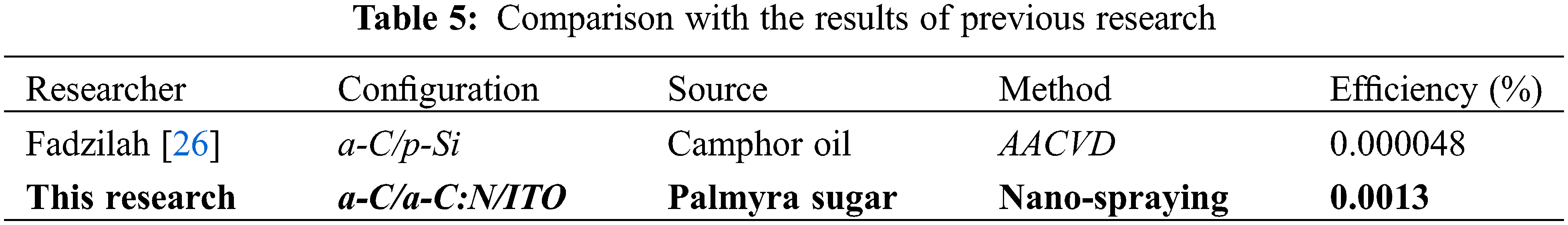
It can be seen in Table 5 that the resulting efficiency increased by two digits compared to that produced by a previous researcher with a similar configuration and different method. This shows that the development of solar cell technology using biomass sources and the nano-spraying method produces better results than the CVD method in a similar configuration. The use of local materials as active materials for solar cell development with this method provides added value to the simplicity of the method, availability of raw materials, low cost and environmentally friendly. Currently, the author and team have developed a solar cell with the same method and materials with the configuration a-C:B/a-C:N/ITO and a-C:B/a-C/a-C:N/ITO and have achieved and an efficiency value of ∼1% and have not yet been published. In subsequent development research, the author and team continue to develop efficiency optimizations produced in the a-C:B/a-C/a-C:N/ITO configuration with a target of achieving an efficiency value of 15% in the next 3–5 years and the capability of commercialization.
The a-C/a-C:N junction sample was successfully deposited through an i-n junction diode to act as a rectifier. It was discovered that the current and voltage values increased when exposed to visible light. This indicates the creation of an electron-hole pair and also shows that the sample is a photodiode. Moreover, the relationship between the current and voltage when illuminated with visible light and directly under sunlight satisfied the photovoltaic cell requirement, and this means the sample can be used as a solar cell with a maximum efficiency of 0.0013%. The liquid palmyra sugar used as the carbon source also shows the possibility of developing solar cells using renewable carbon-active materials. Furthermore, the simple nano-sprayer deposition method applied indicates the potential for developing solar cells through green, inexpensive, easy, and renewable technology.
Acknowledgement: The authors highly appreciate SLRI (public organization) Thailand for providing the PES facilities used in this research. The authors appreciatively acknowledge the Research Council of the University.
Funding Statement: This research was partly funded by the University of Muhammadiyah Malang through a doctoral scientific work development program and also by the Ministry of Finance of Indonesia through the LPDP BUDI-DN scholarship (BP), and National Competitive Fundamental Research Grant (Hibah Penelitian Dasar), Kemendikbudristek, 2021–2022 (D).
Author Contributions: All authors contributed to the process of fabricating, measuring and writing the manuscript.
Availability of Data and Materials: The data that support the findings of this study are openly available in the following sources: Key Engineering Materials (2020), Vol. 860, pp. 185–189. https://doi.org/10.4028/www.scientific.net/KEM.860.185; Key Engineering Materials (2020), Vol. 860, pp. 190–195. https://doi.org/10.4028/www.scientific.net/KEM.860.190; Key Engineering Materials (2020), Vol. 860, pp. 196–201. https://doi.org/10.4028/www.scientific.net/KEM.860.196; Journal Renewable Materials (2021), Vol. 9, No. 6, pp. 1087–1098. https://doi.org/10.32604/jrm.2021.014466.
Conflicts of Interest: The authors declare that they have no conflicts of interest to report regarding the present study.
References
1. Robertson, J. (2002). Diamond like amorphous carbon. Materials Science and Engineering: R: Reports, 37(4–6), 129–281. [Google Scholar]
2. Furlan, K. P., Klein, A. N., Hotza, D. (2013). Diamond like carbon films deposited by hydrocarbon plasma sources. Review Advanced Materials Science, 34, 165–172. [Google Scholar]
3. Zhu, J., Li, F., Liu, G., Liu, D., Li, Q. et al. (2018). Synthesis of amorphous carbon film in ethanol inverse diffusion flames. Nanomaterials, 8(9), 656. [Google Scholar] [PubMed]
4. Li, Z., Cui, C., Zhou, X., Bian, S., Arteaga, O. et al. (2022). Characterization of amorphous carbon films from 5 nm to 200 nm on single-side polished a-plane sapphire substrates by spectroscopic ellipsometry. Frontier in Physics, 10, 965. https://doi.org/10.3389/fphy.2022.968101 [Google Scholar] [CrossRef]
5. Kyle, D. A., Wegener, G., Matthew, D. S., Robert, J. B., Feng, X. et al. (2021). Biogenic formation of amorphous carbon by anaerobic methanotrophs and select methanogens. Science Advances, 7(44), eabg9739. https://doi.org/10.1126/scisdv.abg9739 [Google Scholar] [CrossRef]
6. Neustroev, E. P., Prokopyev, A. R., Semenov, S. O., Popov, V. I., Protopopov, F. F. et al. (2021). Research of properties of a carbon film formed in methane plasma and the following annealing. IOP Conference Series: Materials Science and Engineering, 1079, 042086. https://doi.org/10.1088/1757-899X/1079/4/042086 [Google Scholar] [CrossRef]
7. Zhai, Z., Shen, H., Chen, J., Li, X., Jiang, Y. (2018). Evolution of structural and electrical properties of carbon films from amorphous carbon to nanocrystalline graphene on quartz glass by HFCVD. ACS Applied Materials & Interfaces, 10(20), 17427–17436. https://doi.org/10.1021/acsami.8b01588 [Google Scholar] [PubMed] [CrossRef]
8. Chen, L., Wei, X., Zhang, G., Shang, L., Lu, Z. et al. (2021). Probing the tribological performances of hydrogenated amorphous carbon film in methane atmosphere based on Hertzian elastic contact model. Tribology International, 155, 106790. [Google Scholar]
9. Shinohara, M., Tominaga, T., Shimomura, H., Ihara, T., Yagyu, Y. et al. (2019). Deposition of hydrophilic amorphous carbon film with ether as a source molecule and analysis of its deposition reaction. Electronic and Communication in Japan, 102(4), 3–9. [Google Scholar]
10. Hamdan, A., Makdessi, A. G., Margot, J. (2016). Synthesis of amorphous hydrogenated carbon thin films by magnetized radio-frequency discharge in argon-acetylene mixture at very low gas pressure. Thin Solid Films, 599, 84–97. [Google Scholar]
11. Kamrul, H. M., Kumar, P. B., Hatta, A. (2006). Electrical resistivities of the diamond like carbon films fabricated from methane and acetylene using RF plasma. New Diamond and Frontier Carbon Technology, 16(4), 211–219. [Google Scholar]
12. Ishak, A., Nurrizal, M. A., Rusop, M. (2015). Optical properties of as-deposited amorphous carbon film from various substrate temperatures via custom-made CVD. International Journal of Scientific and Technology Research, 4(1), 257–261. [Google Scholar]
13. Ishak, A., Rusop, M. (2014). Physical properties of nitrogen doped amorphous carbon films from ethanol precursor for solar cell applications. International Journal of Scientific and Technology Research, 3(10), 309–312. [Google Scholar]
14. Pamungkas, D. I., Haikal, A., Bagiya, M. A., Cahyono, Y., Darminto. (2018). Synthesis of amorphous carbon from bio-product by drying method. AIP Conference Proceeding, 1945(1), 020059. [Google Scholar]
15. Pamungkas, D. I., Mukarromah, Priyanto, B., Nakajima, H., Tunmee, S. et al. (2019). Structural analysis and electrical properties of amorphous carbon thin films. Materials Science Forum, 966, 66–71. [Google Scholar]
16. Mukarromah, I., Darminto, D. P. (2019). Structural characterization of amorphous carbon films from palmyra sap. AIP Conference Proceeding, 2120(1), 050011. [Google Scholar]
17. Resplendi, F., Bernardi, M., Cicero, G., Grossman, J. C. (2014). Structure-property relation in amorphous carbon for photovoltaic. Applied Physics Letter, 105, 043903. [Google Scholar]
18. Debajyoti, D., Banerjee, A. (2015). Anti-refection coatings for silicon solar cells from hydrogenated diamond like carbon. Applied Surface Science, 345, 204–215. [Google Scholar]
19. Addie, A. J., Raid, A. I., Mudhafar, A. M. (2022). Amorphous carbon nitride dual-function anti-reflection coating for crystalline silicon solar cells. Scientific Report, 12(1), 1–12. [Google Scholar]
20. Oliviera, Jr. M. H., Silva, D. S., Cortes, A. D. S., Namani, M. A. B., Marques, F. C. (2009). Diamond like carbon used as anti-reflective coating on crystalline silicon solar cells. Diamond & Related Materials, 18, 1028–1030. [Google Scholar]
21. Teixeira, C. O., Andrade, L., Mendes, A. (2019). Novel carbon-based material for perovskite solar cells back-contact. International Journal of Energy Research, 43(13), 7541–7546. [Google Scholar]
22. Bogachuk, D., Tsuji, R., Martineau, D., Narbey, S., Herterich, J. P. et al. (2021). Comparison of highly conductive natural and synthetic graphite foe electrodes in perovskite solar cells. Carbon, 178, 10–18. [Google Scholar]
23. Adhikari, S., Kayastha, M. S., Ghimire, D. C., Aryal, H. R., Adhikary, S. et al. (2013). Improved photovoltaic properties of heterojunction carbon based solar cell. Journal of Surface Engineered Materials and Advanced Technology, 3, 178–183. [Google Scholar]
24. Khan, R. U. A., Silva, S. R. P., Van Swaij, R. A. C. M. M. (2003). Polymeric amorphous carbon as p-type window within amorphous silicon solar cells. Applied Physics Letter, 82(22), 3979–3981. [Google Scholar]
25. Ahmad, N., Kamaruzzaman, D., Rusop, M. (2012). Amorphous carbon deposited by novel aerosol assisted chemical vapor deposition for photovoltaic solar cells. Japanese Journal of Applied Physics, 51(6S), 06FD05. [Google Scholar]
26. Fadzilah, A. N., Dayana, K., Rusop, M. (2012). Carbon-based solar cell from amorphous carbon with nitrogen incorporation. Advanced Materials Research, 576, 785–788. [Google Scholar]
27. Zhao, X., Wu, H., Yang, L., Wu, Y., Sun, Y. et al. (2019). High efficiency CNT-Si heterojunction solar cells by dry gas doping. Carbon, 147, 164–171. [Google Scholar]
28. Eguchi, T., Kato, S., Kishi, N., Soga, T. (2022). Effect of thickness on photovoltaic properties of amorphous carbon/fullerene junction. AIMS Materials Science, 9(3), 446–454. [Google Scholar]
29. Soga, T., Nakagaki, T., Kato, S., Kishi, N. (2018). Effect of sublimation of temperature on the photovoltaic properties of amorphous carbon thin film from fullerene. Journal of Solar Energy Research Update, 5, 8–13. [Google Scholar]
30. Wei, D., Liu, Y., Wang, Y., Zhang, H., Huang, L. et al. (2009). Synthesis of N-doped graphene by chemical vapor deposition and electrical properties. Nano Letter, 9(5), 1752–1758. [Google Scholar] [PubMed]
Cite This Article
 Copyright © 2024 The Author(s). Published by Tech Science Press.
This work is licensed under a Creative Commons Attribution 4.0 International License , which permits unrestricted use, distribution, and reproduction in any medium, provided the original work is properly cited.
 Downloads
 Citation Tools