
 Submit a Paper
 Propose a Special lssue
 Open Access
ARTICLE

Synthesis and Photoresponse of Quinary Zinc-Blende Cu3FeInSnS6 Nanoplates
1 School of Pharmaceutical Sciences, Changchun University of Chinese Medicine, Changchun, China
2 Academy of Aviation Operation Service, Aviation University of Air Force, Changchun, China
* Corresponding Authors: Haixia Yu. Email: ; Lingkun Meng. Email:
# These authors contributed equally to this work
Chalcogenide Letters 2026, 23(1), 3 https://doi.org/10.32604/cl.2026.075922
Received 11 November 2025; Accepted 12 January 2026; Issue published 26 January 2026
 View Full Text
 Download PDF
Abstract
Quinary Cu3FeInSnS6 (CFITS) nanoplates were synthesized through a synergistic dual-cation substitution strategy using a hot-injection method, where oleylamine and 1-dodecanethiol served as coordinating ligands to guide two-dimensional growth. The nanocrystals were characterized by X-ray diffraction, transmission electron microscopy, X-ray photoelectron spectroscopy, and absorption spectroscopy. Structural analysis confirms that the CFITS nanoplates crystallize in a phase-pure cubic zinc-blende structure (space group F-43 m) without detectable secondary phases. Optical measurements reveal that the nanoplates exhibit broad and intense visible-light absorption with a direct bandgap of 1.51 ± 0.03 eV, suitable for photovoltaic applications. Under standard AM 1.5 G illumination, the CFITS film shows a clear photoresponse with a light-to-dark current ratio (Ilight/Idark) of 2.46, surpassing several related copper-based chalcogenides. This enhancement is attributed to the synergistic substitution of Fe2+ and In3+, which is proposed to effectively suppress antisite defects and improve charge transport. Furthermore, the two-dimensional geometry endows the nanoplates with a unique electronic structure that mitigates carrier recombination and facilitates interfacial charge extraction. The solution-processable CFITS nanoplate films demonstrate good atmospheric stability, maintaining performance over 24 h. This work not only expands the family of multinary copper chalcogenides but also provides a feasible strategy for designing efficient, low-cost, and earth-abundant absorber materials for next-generation thin-film solar cells.Keywords
Supplementary Material
Supplementary Material FileCopper-based thin films stand out as a prime candidate for the absorber layers in the next generation of thin-film solar cells, possessing a range of advantages such as high absorption coefficients, broad solar spectrum coverage, and robust stability under solar irradiation, thus garnering significant attention [1,2,3,4]. Among them, multinary copper-based chalcogenide nanocrystals (NCs) represent a distinctive category of absorptive materials. They offer the flexibility to tailor composition, structure, and morphology, thereby enabling controlled band gaps and optical properties, which has drawn considerable research interest [5,6,7,8,9].
Copper zinc tin sulphur (Cu2ZnSnS4, CZTS), a quaternary compound, attracts particular attention as a thin film photovoltaic absorber, owing to its abundant constituent elements, environmentally friendly nature, high absorption coefficients, and ideal direct band gaps [10,11]. However, its highest recorded efficiency currently stands at 12.6%, which remains significantly lower than the theoretical Shockley–Queisser limit of 32.4% for CZTS [12,13,14]. It has been suggested that the easy formation of detrimental antisite defects in CZTS, such as ZnCu, maybe the primary factor contributing to the low power conversion efficiency (PCE) in CZTS-based solar cells, even in high-quality single-crystal CZTSSe [15,16,17,18,19]. The strategic incorporation of indium (In) into CZTS has been demonstrated as an effective approach for suppressing antisite defects. Jiang et al. achieved a power-conversion efficiency of 6.9% by post-annealing the In2S3–CZTS heterojunction [20]. The treatment drove In diffusion into CZTS, generating benign InZn donors while concurrently suppressing deleterious antisite defects. Korade et al. demonstrated that In incorporation into CZTSSe thin films significantly improved device performance (9.53%) and Voc (486 mV) compared to undoped counterparts (8.31%, 467 mV) [21]. The In-doped devices exhibited enhanced crystal growth, suppressed nonradiative recombination, and improved carrier separation and transport. However, complete elimination of ZnCu antisite defects remains unachieved through In doping alone. Complementarily, isovalent cation substitutions are recognized as another effective approach to suppress the formation of ZnCu disorder in CZTS [15,17,22]. The replacement of Zn with Fe in CZTS thin films is believed to be a promising strategy [23,24,25]. This substitution not only optimizes the optical band gap energy but also improves conductivity and the efficiency of solar-to-electricity conversion. Building upon these findings, we propose that coordinated implementation of In incorporation coupled with Fe substitution at Zn sites could synergistically modulate defect thermodynamics and optimize electronic performance, offering a promising pathway toward developing new photovoltaic absorber materials—Cu3FeInSnS6. Nevertheless, the specific quinary compound resulting from this dual strategy has remained unexplored to date in materials science.
The broader landscape of quinary copper chalcogenides has primarily focused on isolated cation cross-substitutions or anion mixing strategies, as exemplified by recent studies on Cu3ZnInSnS(Se)6 [26,27], and Cu2ZnSn(S,Se)4 [28,29]. The simultaneous incorporation of both heterovalent In3+ and isovalent Fe2+ within a single-phase quinary structure—to date—has not been investigated. This compositional space presents a promising, underexplored path for developing new photovoltaic absorbers. By moving beyond traditional quaternary systems, it focuses on inherent defect depression, with the additional potential to improve carrier separation and transport.
The morphology of the NCs has significant impact on the performance of NC-based devices. Two-dimensional (2D) copper-based chalcogenides have demonstrated notable advantages in the field of photoelectric conversion [30,31]. The high surface area and quantum confinement effects of 2D nanoplates enhance light absorption, enabling more efficient utilization of the solar spectrum. These nanoplates also feature a unique electronic structure and reduced dimensionality, which significantly improve charge carrier transport and reduce recombination losses. Furthermore, their atomically smooth surfaces and well-defined interfaces minimize interfacial defects, thereby boosting charge extraction and overall device efficiency. With these combined advantages, 2D nanoplate morphologies are highly suitable as light-absorbing layers in solar cells. Coordinating ligands can significantly influence NC morphology through their adsorption onto partially charged facets. The use of oleylamine (OLA) and 1-dodecanethiol (DDT) is beneficial for achieving 2D morphologies in copper-based chalcogenides, as OLA passivates basal planes and DDT forms lamellar complexes that template 2D growth, as evidenced in the literature [32,33,34,35].
In this study, leveraging the insights from synergistic material design [36] and the importance of microstructural precision [37], we develop an integrated strategy combining dual-cation modulation with 2D morphology control to synthesize the novel quinary Cu3FeInSnS6 (CFITS) nanoplates. This work represents the first experimental realization of synergistic dual-cation defect depression engineering (via Fe and In substitution) in a morphology-optimized 2D architecture. The resulting NCs crystallize in a cubic zinc-blende structure and exhibit strong, broadband optical absorption across the visible region—a key characteristic for an efficient light absorber. Notably, thin films fabricated from these NCs demonstrate a clear photoresponse, highlighting that CFITS nanoplates are promising candidates for use as the light-absorbing layer in thin-film solar cells.
CuCl2 (99.99%), FeCl2 (99.5%), thiourea (99%) and OLA (80–90%) were purchased from Aladdin; anhydrous SnCl2 (99.99%), InCl3 (99.99%), DDT (98%) were obtained from Alfa Aesar. Ethanol (AR) and toluene (AR) were acquired from Beijing Chemical Reagent Company.
The synthesis of CFITS nanoplates was carried out using a modified hot-injection protocol, wherein thiourea solution was swiftly introduced into a pre-heated metal precursor mixture under inert nitrogen (N2) atmosphere. Typically, a mixture of metal chloride precursors—CuCl2 (0.300 mmol), FeCl2 (0.100 mmol), InCl3 (0.100 mmol), and SnCl2 (0.100 mmol)—was combined with 10.00 mL of OLA and 1.00 mL of DDT in a three-necked flask. The mixture was heated to 120°C and then subjected to N2 purge. Subsequently, the temperature was raised to 160°C, and 1.80 mL of a 0.50 M thiourea solution in OLA was swiftly injected. The reaction was then heated to 230°C and maintained for 60 min. After cooling to room temperature, the NCs were purified by ethanol-induced precipitation. Finally, the product was redispersed in toluene.
CFITS NC films were fabricated by spin-coating a concentrated toluene dispersion onto glass slides, followed by drying under ambient conditions, post-annealing at 350°C for 5 min on a hotplate in a N2 atmosphere, and finally evaporating two aluminum (Al) electrodes.
X-ray diffraction (XRD) patterns were acquired on a Bruker D8 diffractometer (Cu Kα radiation, λ = 1.54 Å). For reference, simulated powder XRD patterns were generated using Diamond 3.0 software. Chemical composition was determined by inductively coupled plasma mass spectroscopy (ICP-MS, Thermo Jarrell-Ash). Surface electronic states were analyzed by X-ray photoelectron spectroscopy (XPS) on a VG ESCALAB MKII spectrometer. Optical absorption was measured with a Shimadzu UV-3600 spectrophotometer. Microstructural and elemental analyses were performed by transmission electron microscopy (TEM) and associated techniques using a JEOL JEM-2010 instrument (operated at 200 kV). This included high-resolution TEM (HRTEM), energy-dispersive X-ray spectroscopy (EDS), and elemental mapping, with EDS specimens prepared on carbon-coated nickel grids. Finally, the electrical performance was evaluated by measuring current-voltage (I-V) characteristics with a Keithley 2400 source meter, both in the dark and under simulated AM 1.5 G illumination (100 mW cm−2) provided by an Abet Sun 2000 solar simulator.
The 2D CFITS nanoplates were synthesized via a hot-injection method, wherein a solution of thiourea in OLA was rapidly injected into a mixed precursor solution containing CuCl2, FeCl2, InCl3, and SnCl2 at a molar ratio of 3:1:1:1, dissolved in OLA and DDT. DDT was introduced to minimize precursor reactivity mismatch and promote the growth of a 2D morphology.
Fig. 1 presents the XRD pattern of the as-synthesized CFITS NCs. The relatively broad diffraction peaks indicate their nanocrystalline nature, consistent with TEM observations, and the profile closely matches that of the cubic zinc-blende ZnS phase [38,39]. Using this phase as a model, a simulation was performed with Diamond 3.0 software. The agreement between the experimental and simulated patterns confirms that the CFITS NCs crystallize in a zinc-blende structure with the F-43m space group. The calculated lattice parameter is a = 5.5320 Å. Furthermore, no diffraction peaks from secondary phases (e.g., Cu2S, FeS, or SnS2) are detected within the instrument’s resolution limit.
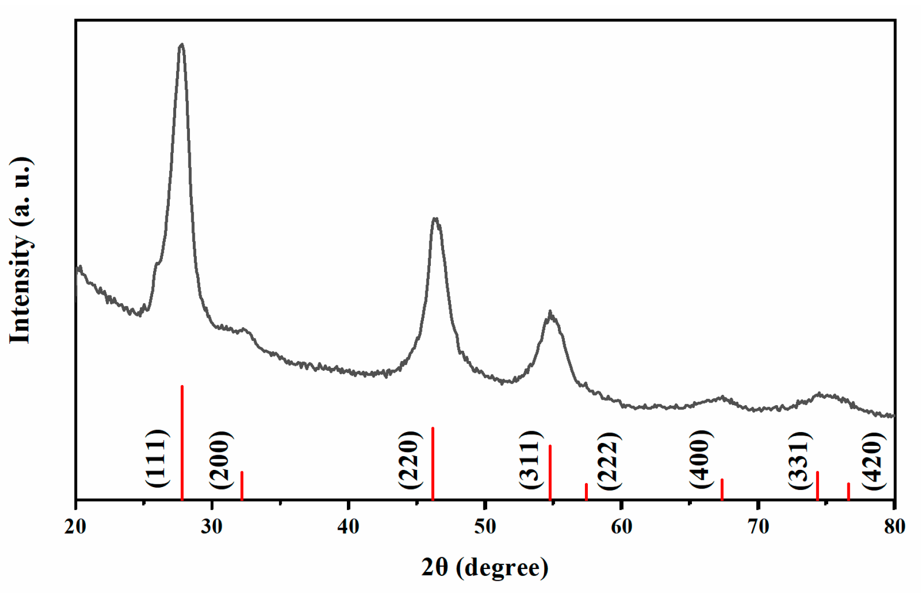
Figure 1: The experimental (black) and simulated (red) XRD patterns of zinc-blende CFITS NCs.
Fig. 2a shows a TEM image of well-separated CFITS NCs. These NCs display the 2D triangular and hexagonal platelet shape with average side lengths of 44.5 ± 5.9 nm and 18.1 ± 2.2 nm, respectively. This coexistence of two morphologies has also been documented in previous literature [40,41]. Since it can improve contacts and make charge transfer between NCs easier, the plate-like shape may be significant in the production of NC solids for device applications. The lattice fringes with a spacing of 0.320 nm in the HRTEM image (Fig. 2b) correspond to the (111) planes of the zinc-blende CFITS, which agrees with the XRD results.
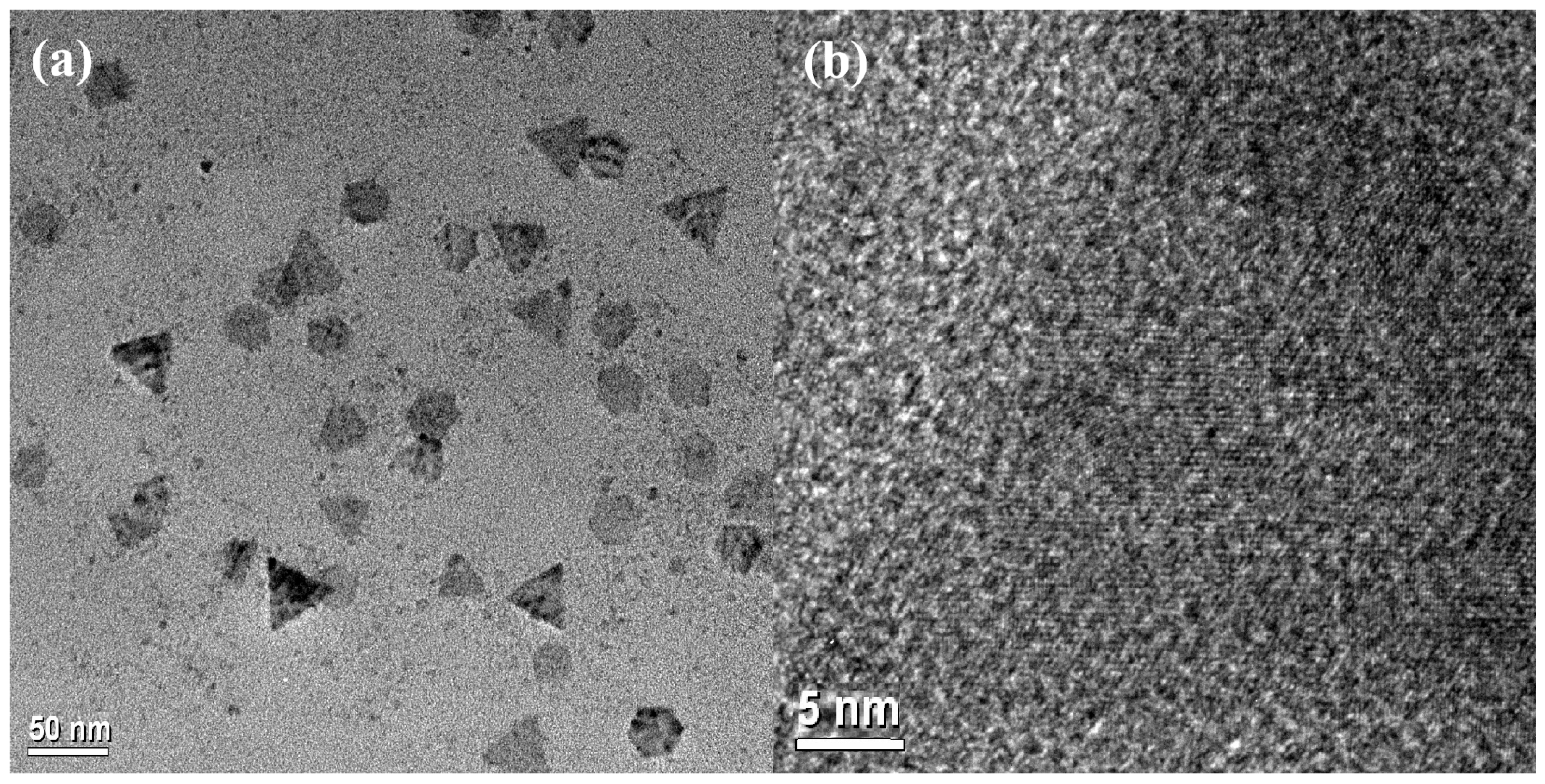
Figure 2: TEM (a) and HRTEM (b) images of CFITS NCs.
The compositional analyses presented in Fig. S1 and Table S1, obtained via EDS and ICP-MS measurements, reveal an elemental ratio of Cu:Fe:In:Sn:S of approximately 3:1:1:1:6. To further confirm the homogeneous distribution of each element within the as-synthesized nanoplates, scanning transmission electron microscopy (STEM)-EDS elemental mapping was employed to study the distribution of each element in the as-synthesized CFITS NCs. The results illustrated in Fig. 3 reveal that all elements are uniformly dispersed throughout the nanoplates, with no significant segregation detectable, indicating that CFITS nanoplates are homogeneously alloyed.
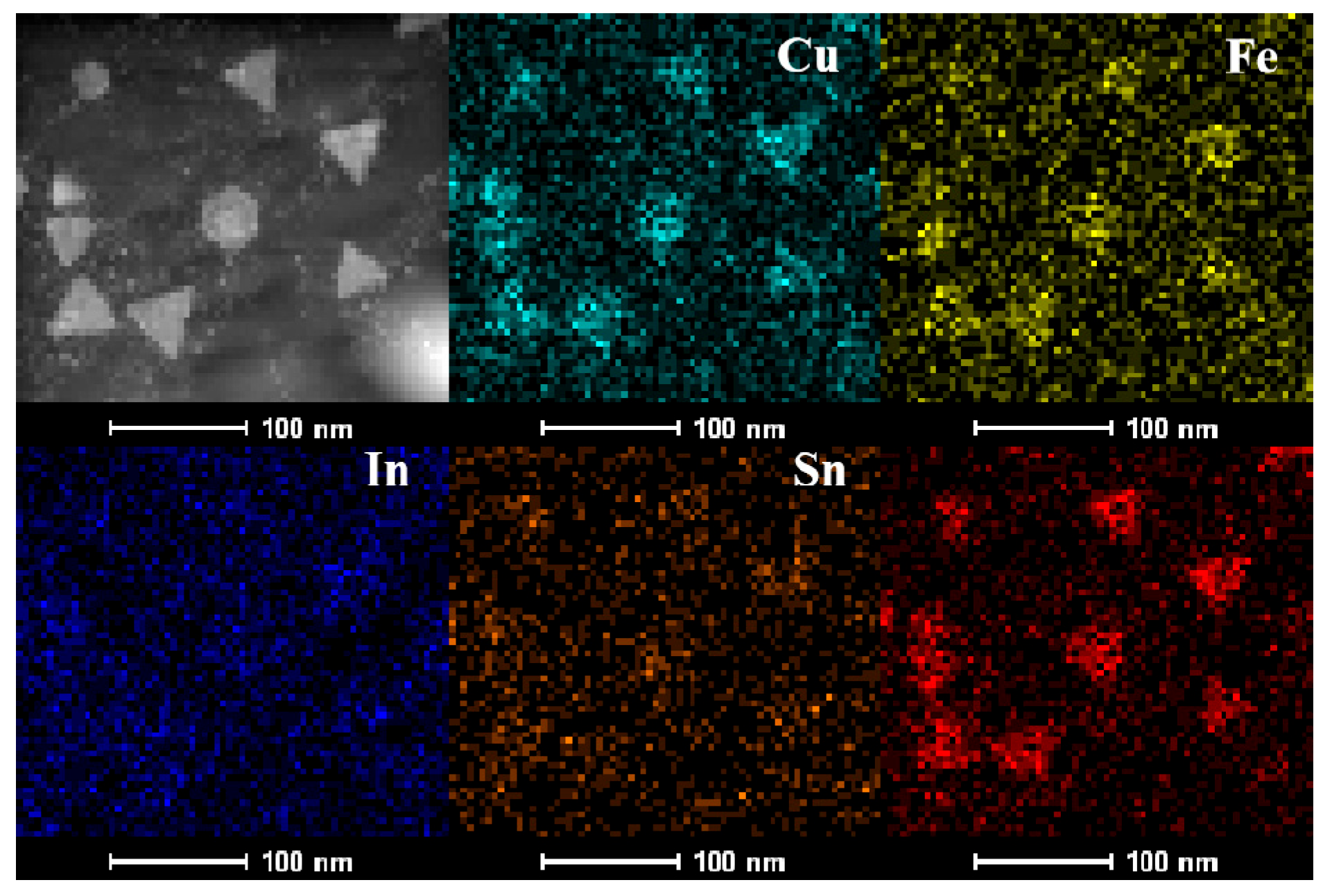
Figure 3: HAADF STEM image of CFITS nanoplates, and corresponding elemental mapping images.
Fig. S2 illustrates the XPS spectrum of Cu 2p, Fe 2p, In 3d, Sn 3d, and S 2p. The XPS spectra were deconvoluted to better understand the underlying chemical states. The copper spectrum displays two peaks at 931.7 eV and 951.5 eV with a peak separation of 19.8 eV, which is in good accordance with the value of Cu (I). Fe (II) is suggested by the Fe 2p peaks at 711.3 and 724.9 eV, which have a peak separation of 13.6 eV. The In 3d spectrum is characterized by two peaks at 444.25 eV and 451.75 eV, assignable to In3+ in the NCs. The Sn (IV) state is confirmed by peaks located at 494 and 485.5 eV with its characteristic peak separation of 8.5 eV. The presence of S 2p peaks at 161.7 and 162.9 eV suggests that the element is in the S2− state. These results are in accordance with the previously reported values in the literature [42,43].
Fig. 4 presents the electronic absorption spectra of the as-synthesized CFITS nanoplates, indicating a broad absorption covering the ultraviolet (UV) to visible and near-infrared (NIR) regions. By extrapolating the linear region of the Tauc plot, where (αhν)2 (α for absorption coefficient, hν for photon energy) is plotted versus hν, the band gap (Eg) of CFITS nanoplates is estimated to be 1.51± 0.03 eV, as shown in the inset of Fig. 4. Photoresponse of the obtained zinc-blende CFITS nanoplates has been investigated to assess their potential as an active layer for solar applications. Fig. 5 shows the current-voltage (I-V) curves measured for the CFITS thin films in dark and under light irradiation. The Ilight/Idark ratio of the sample was around 2.46. The photoresponsive behaviour is obvious, suggesting the as-synthesised CFITS nanoplates could be a viable option for an absorbing layer material. Table 1 compares this work with the literature for photoresponse. CFITS nanoplate films represent a measurable improvement over some prior results for CZTS, CFTS, or CZITS-based NC films [26,44,45]. This gain can be attributed to the dual-cation modulation strategy adopted here, which may effectively mitigates ZnCu antisite defects and enhances carrier mobility. Additionally, the atmospheric stability of the synthesized CFITS NC films was also investigated. As shown in the Fig. S3, the Ilight of the CFITS films remains nearly constant within the first 24 h, with only a slight decrease observed after several days, indicating their relatively good stability. The observed decline of Ilight may be mitigated through strategies such as ligand exchange—for example, by using cobalt β-tetraaminophthalocyanine. This approach will be further explored in our subsequent work.
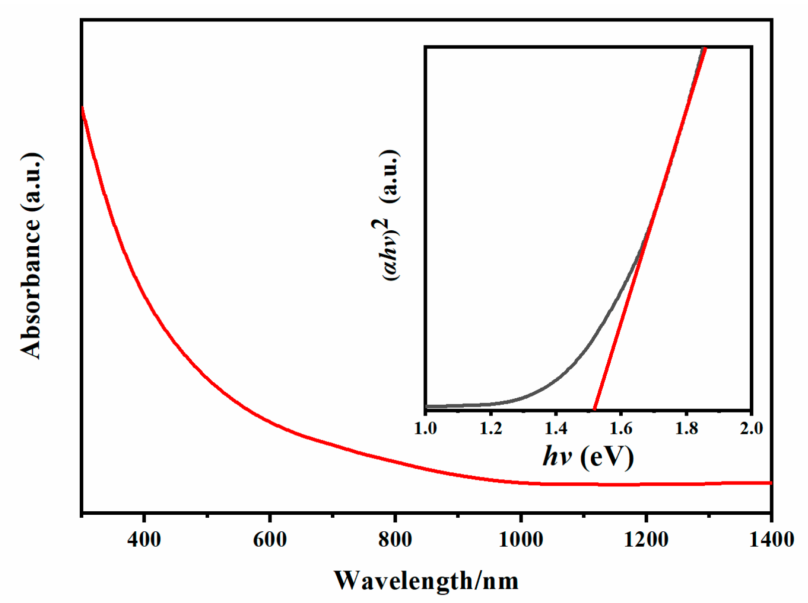
Figure 4: UV-Vis-NIR absorption spectrum of CFITS nanoplates. The inset shows the Tauc plot for energy band gap extraction.
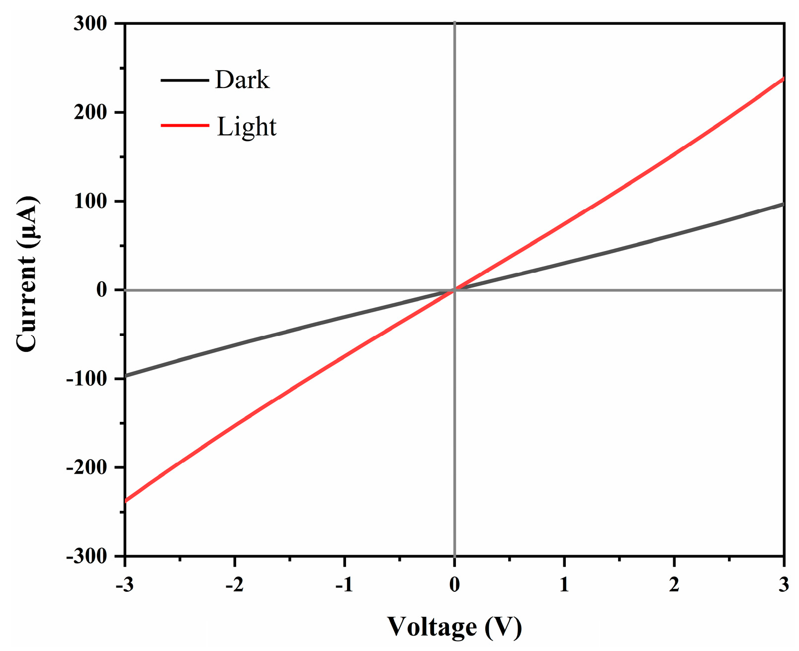
Figure 5: I–V curves of spin-casting film built from CFITS nanoplates: in the dark (black) and under simulated solar light illumination (red).
In summary, this work successfully synthesized quinary CFITS nanoplates via a hot-injection method, employing a dual-cation engineering strategy that simultaneously suppresses antisite defects and enhances charge transport. The resulted CFITS demonstrates potential for improved defect depression through cations substitution, a relatively high photoresponse (Ilight/Idark = 2.46), and a solution-processable 2D morphology beneficial for interfacial charge extraction. The synergy between heterovalent In3+ and isovalent Fe2+ substitution in this morphology-optimized system demonstrates an effective route to advance copper-based absorbers. Future research will focus on fabricating complete photovoltaic devices with optimized junction partners (e.g., CdS, ZnO), ligands exchanging to improve stability, and conducting theoretical modelling of defect formation energies to guide further composition optimization. This study positions CFITS as a promising earth-abundant absorber candidate for thin-film photovoltaics, extending material design beyond classical quaternary systems and offering a feasible direction toward efficient, low-cost solar energy conversion.
Acknowledgement:
Funding Statement: This work was supported by Science and Technology Development Plan of Jilin Province (No. YDZJ202301ZYTS187) and College Student Innovation and Entrepreneurship Training Program (No. S202410199025, S202510199031).
Author Contributions: Dehui Li: Writing-original draft, Methodology, Investigation, Data curation, Funding acquisition. Yiming Guo: Validation, Software, Investigation, Formal analysis. Tao He: Resources, Investigation, Formal analysis. Binbin Zhang: Software, Data curation, Haixia Yu: Investigation, Formal analysis, Supervision. Lingkun Meng: Writing—Review & Editing, Resources, Funding acquisition, Supervision. All authors reviewed and approved the final version of the manuscript.
Availability of Data and Materials: Data will be made available on request.
Ethics Approval: Not applicable.
Conflicts of Interest: The authors declare no conflicts of interest.
Supplementary Materials: The supplementary material is available online at https://www.techscience.com/doi/10.32604/cl.2026.075922/s1. Supplementary Figure S1: EDS of CFITS nanoplates. The relative elemental ratios for Cu:Fe:In:Sn:S are 3.16:1:1.13:1.01:6.27. The C, O and Ni signals result from the carbon substrate. The observed Si signal is from the Si detector. Supplementary Figure S2: XPS spectra of CFITS nanoplates. Supplementary Figure S3: I–V characteristics of a CFITS thin film at varying exposure times to air. Supplementary Table S1: The overall element ratios of CFITS nanoplates determined by ICP-MS analysis.
References
1. Xing C, Lei Y, Liu M, Wu S, He W, Zheng Z. Environment-friendly Cu-based thin film solar cells: materials, devices and charge carrier dynamics. Phys Chem Chem Phys. 2021;23(31):16469–87. doi:10.1039/D1CP02067F. [Google Scholar] [CrossRef]
2. Sajitha DR, Stephen B, Nakamura A, Selvaraj M, Salammal ST, Hussain S. The emergence of chalcogenides: a new era for thin film solar absorbers. Prog Solid State Chem. 2024;76:100490. doi:10.1016/j.progsolidstchem.2024.100490. [Google Scholar] [CrossRef]
3. Amrillah T, Prasetio A, Supandi AR, Sidiq DH, Putra FS, Nugroho MA, et al. Environment-friendly copper-based chalcogenide thin film solar cells: status and perspectives. Mater Horiz. 2023;10(2):313–39. doi:10.1039/D2MH00983H. [Google Scholar] [CrossRef]
4. Li W, Tan JMR, Leow SW, Lie S, Magdassi S, Wong LH. Recent progress in solution-processed copper-chalcogenide thin-film solar cells. Energy Technol. 2018;6(1):46–59. doi:10.1002/ente.201700734. [Google Scholar] [CrossRef]
5. Shi J, Wang J, Meng F, Zhou J, Xu X, Yin K, et al. Multinary alloying for facilitated cation exchange and suppressed defect formation in kesterite solar cells with above 14% certified efficiency. Nat Energy. 2024;9(9):1095–104. doi:10.1038/s41560-024-01551-5. [Google Scholar] [CrossRef]
6. Palchoudhury S, Ramasamy K, Gupta A. Multinary copper-based chalcogenide nanocrystal systems from the perspective of device applications. Nanoscale Adv. 2020;2(8):3069–82. doi:10.1039/D0NA00399A. [Google Scholar] [CrossRef]
7. Wu XJ, Huang X, Qi X, Li H, Li B, Zhang H. Copper-based ternary and quaternary semiconductor nanoplates: templated synthesis, characterization, and photoelectrochemical properties. Angew Chem Int Ed. 2014;53(34):8929–33. doi:10.1002/anie.201403655. [Google Scholar] [CrossRef]
8. Ledesma-Juárez A, Quintero-Guerrero JF, Fernández AM. Fabrication and characterization of Cu(In,Ga)Se2 thin films by electrodeposition: optimization of the thermal treatment with selenium and mechanical disturbance technique. Chalcogenide Lett. 2025;22(2):97–108. doi:10.15251/CL.2025.222.97. [Google Scholar] [CrossRef]
9. Haouanoh D, Toubane M, Talaighil R, Bensouici F. Chemical bath deposition of CZTS layers; study of pH, time deposition and annealing temperature effects. Chalcogenide Lett. 2025;22(2):177–88. doi:10.15251/CL.2025.222.177. [Google Scholar] [CrossRef]
10. Ali Shah U, Wang A, Irfan Ullah M, Ishaq M, Shah IA, Zeng Y, et al. A deep dive into Cu(2)ZnSnS(4) (CZTS) solar cells: a review of exploring roadblocks, breakthroughs, and shaping the future. Small. 2024;20(30):e2310584. doi:10.1002/smll.202310584. [Google Scholar] [CrossRef]
11. Amrillah T. Enhancing the value of environment-friendly CZTS compound for next generation photovoltaic device: a review. Sol Energy. 2023;263:111982. doi:10.1016/j.solener.2023.111982. [Google Scholar] [CrossRef]
12. Lie S, Leow SW, Bishop DM, Guc M, Izquierdo-Roca V, Gunawan O, et al. Improving carrier-transport properties of CZTS by Mg incorporation with spray pyrolysis. ACS Appl Mater Interfaces. 2019;11(29):25824–32. doi:10.1021/acsami.9b05244. [Google Scholar] [CrossRef]
13. Yang X, Qin X, Yan W, Zhang C, Zhang D. Effects of Fe and Ni doping on the electronic structure and optical properties of Cu2ZnSnS4. Crystals. 2023;13(7):1082. doi:10.3390/cryst13071082. [Google Scholar] [CrossRef]
14. Zakaria S, El mahboub E, EL Hichou A. Physical properties of the low-cost CZTS absorber layer deposited by spin-coating: effect of the copper concentration associated with SCAPS-1D simulation. RSC Adv. 2023;13(39):27106–15. doi:10.1039/D3RA03996J. [Google Scholar] [CrossRef]
15. Kangsabanik M, Gayen RN. A comprehensive review on the recent strategy of cation substitution in CZTS(Se) thin films to achieve highly efficient kesterite solar cells. Sol RRL. 2023;7(24):2300670. doi:10.1002/solr.202300670. [Google Scholar] [CrossRef]
16. Li J, Wang D, Li X, Zeng Y, Zhang Y. Cation substitution in earth-abundant kesterite photovoltaic materials. Adv Sci. 2018;5(4):1700744. doi:10.1002/advs.201700744. [Google Scholar] [CrossRef]
17. Kumar MS, Madhusudanan SP, Batabyal SK. Substitution of Zn in Earth-Abundant Cu2ZnSn(S,Se)4 based thin film solar cells—a status review. Sol Energy Mater Sol Cells. 2018;185:287–99. doi:10.1016/j.solmat.2018.05.003. [Google Scholar] [CrossRef]
18. Espinel Pérez NM, Vera López E, Gómez Cuaspud JA, Carda Castelló JB. A review of recent advances of kesterite thin films based on magnesium, iron and nickel for photovoltaic application: insights into synthesis, characterization and optoelectronic properties. Clean Energy. 2024;8(2):217–38. doi:10.1093/ce/zkad093. [Google Scholar] [CrossRef]
19. Gokmen T, Gunawan O, Todorov TK, Mitzi DB. Band tailing and efficiency limitation in kesterite solar cells. Appl Phys Lett. 2013;103(10):103506. doi:10.1063/1.4820250. [Google Scholar] [CrossRef]
20. Jiang F, Ozaki C, Gunawan, Harada T, Tang Z, Minemoto T, et al. Effect of indium doping on surface optoelectrical properties of Cu2ZnSnS4 photoabsorber and interfacial/photovoltaic performance of cadmium free In2S3/Cu2ZnSnS4 heterojunction thin film solar cell. Chem Mater. 2016;28(10):3283–91. doi:10.1021/acs.chemmater.5b04984. [Google Scholar] [CrossRef]
21. Korade SD, Gour KS, Karade VC, Jang JS, Rehan M, Patil SS, et al. Improving the device performance of CZTSSe thin-film solar cells via indium doping. ACS Appl Mater Interfaces. 2023;15(49):57183–91. doi:10.1021/acsami.3c13813. [Google Scholar] [CrossRef]
22. Abdillah N, Ayukaryana NR, Agusta MK, Rusydi F, Shukri G. On the thermodynamic of Cu-Zn disorder formation and electronic structure changes of alkaline-earth M-doped kesterite Cu2ZnSnS4 (M = Be, Mg, Ca). Mater Chem Phys. 2025;332:130262. doi:10.1016/j.matchemphys.2024.130262. [Google Scholar] [CrossRef]
23. Kalambur S, Mouli R, Choudhari NJ, Kavya DM, Raviprakash Y. Exploring the potential of Cu2FeSnS4: a comprehensive review on structural properties, optoelectronic features, and future prospects in earth-abundant thin film solar cells. Cogent Eng. 2024;11(1):2322076. doi:10.1080/23311916.2024.2322076. [Google Scholar] [CrossRef]
24. Muñoz-Malpica JH, Espitia-Mayorga MI, Cerón-Achicanoy MA, Gómez-Cuaspud JA, Vera-López E. Time dependence in the synthesis of Cu2FeSnS4 and some of its properties. Dyna. 2023;90(225):147–55. doi:10.15446/dyna.v90n225.104457. [Google Scholar] [CrossRef]
25. Hussein HM. Comparative study between spin coated Cu2ZnSnS4 and Cu2FeSnS4 thin films for thin-film solar cell applications. Appl Sol Energy. 2022;58(6):751–9. doi:10.3103/S0003701X22060081. [Google Scholar] [CrossRef]
26. Li D, Sun J, Zhao X, Yang X. Synthesis and phase transition of wurtzite Cu3ZnInSnS6 nanodisks. Nanoscale. 2015;7(31):13191–5. doi:10.1039/C5NR02950C. [Google Scholar] [CrossRef]
27. Li D, Sun J, Zhao X, Ma X, Yang X. Facile synthesis and optical properties of zincblende and wurtzite Cu3ZnInSnSe6 nanocrystals. J Alloys Compd. 2016;689:425–31. doi:10.1016/j.jallcom.2016.07.232. [Google Scholar] [CrossRef]
28. Zhao J, Liang GX, Hu JG, Zheng ZH, Luo JT, Zhang DP, et al. Substrate temperature-assisted preparation of CZTSSe thin films by a single quinary target. J Electron Mater. 2018;47(1):873–8. doi:10.1007/s11664-017-5881-2. [Google Scholar] [CrossRef]
29. Braun MB, Korala L, Kephart JM, Prieto AL. Synthetic control of quinary nanocrystals of a photovoltaic material: the clear role of chalcogen ratio on light absorption and charge transport for Cu2–xZn1+xSn(S1–ySey)4. ACS Appl Energy Mater. 2018;1(3):1053–9. doi:10.1021/acsaem.7b00198. [Google Scholar] [CrossRef]
30. Yuan H, Wang H, Cui Y. Two-dimensional layered chalcogenides: from rational synthesis to property control via orbital occupation and electron filling. Acc Chem Res. 2015;48(1):81–90. doi:10.1021/ar5003297. [Google Scholar] [CrossRef]
31. Kapuria N, Patil NN, Ryan KM, Singh S. Two-dimensional copper based colloidal nanocrystals: synthesis and applications. Nanoscale. 2022;14(8):2885–914. doi:10.1039/D1NR06990J. [Google Scholar] [CrossRef]
32. Das Adhikari S, Dutta A, Prusty G, Sahu P, Pradhan N. Symmetry break and seeded 2D anisotropic growth in ternary CuGaS2 nanocrystals. Chem Mater. 2017;29(12):5384–93. doi:10.1021/acs.chemmater.7b01775. [Google Scholar] [CrossRef]
33. van der Stam W, Rabouw FT, Geuchies JJ, Berends AC, Hinterding SOM, Geitenbeek RG, et al. In situ probing of stack-templated growth of ultrathin Cu2–xS nanosheets. Chem Mater. 2016;28(17):6381–9. doi:10.1021/acs.chemmater.6b02787. [Google Scholar] [CrossRef]
34. Coughlan C, Guo Y, Singh S, Nakahara S, Ryan KM. Synthesis of curved CuIn1–xGax(S1–ySey)2 nanocrystals and complete characterization of their diffraction contrast effects. Chem Mater. 2018;30(23):8679–89. doi:10.1021/acs.chemmater.8b04082. [Google Scholar] [CrossRef]
35. Liu Y, Yin D, Swihart MT. Valence selectivity of cation incorporation into covellite CuS nanoplatelets. Chem Mater. 2018;30(4):1399–407. doi:10.1021/acs.chemmater.7b05198. [Google Scholar] [CrossRef]
36. Chen X, Lv S, Liu Y, Gu H, Sun X, Hu Q, et al. Antiferroelectric SnO2 network with amorphous surface for electrochemical N2 fixation. Angew Chem Int Ed. 2025;64(43):e202515222. doi:10.1002/anie.202515222. [Google Scholar] [CrossRef]
37. Liang J, Ye F, Song Q, Cao Y, Xiao C, Qin Y, et al. Genetic algorithm designed multilayered Si3N4 nanowire membranes hybridized by dielectric wide-range tunable CVD graphene skin for broadband microwave absorption. Compos Part B Eng. 2025;297:112298. doi:10.1016/j.compositesb.2025.112298. [Google Scholar] [CrossRef]
38. Thiodjio Sendja B, Tchana Kamgne D, Aquilanti G, Olivi L, Plaisier JR. Low-range thermal investigation of zincblende-type ZnS by combined extended X-ray absorption fine structure and X-ray diffraction techniques. Phys B Condens Matter. 2018;545:481–90. doi:10.1016/j.physb.2018.06.005. [Google Scholar] [CrossRef]
39. Marusamy A, Agilan S, Muthukumarasamy N, Sentil Kumaran CK, Saravanakumar M. The influence of the Zn/S source concentration ratio on its structural, optical and magnetic properties of ZnS quantum dots. Chalcogenide Lett. 2013;10(5):179–87. [Google Scholar]
40. Pang C, Yang R, Singh A, Chen H, Bowman MK, Bao N, et al. Colloidal synthesis and magnetic properties of anisotropic-shaped spinel CuCr2Se4 nanocrystals. RSC Adv. 2017;7(50):31173–9. doi:10.1039/C7RA03473C. [Google Scholar] [CrossRef]
41. Lesyuk R, Klein E, Yaremchuk I, Klinke C. Copper sulfide nanosheets with shape-tunable plasmonic properties in the NIR region. Nanoscale. 2018;10(44):20640–51. doi:10.1039/C8NR06738D. [Google Scholar] [CrossRef]
42. Bian Q, Liao H, Tang C, Li K, Wan J, Xiao Y, et al. Sulfur-source-dependent phase-selective preparation of Cu(3)NiInSnS(6) nanocrystals and their optical and magnetic properties. Dalton Trans. 2022;51(30):11416–26. doi:10.1039/D2DT01643E. [Google Scholar] [CrossRef]
43. Abbas A, Li K, Guo X, Wu A, Song C, Yang H, et al. Influence of surfactant-assisted synthesis and different operational parameters on photocatalytic performance of Cu2FeSnS4 particles. Surf Interfaces. 2021;24:101134. doi:10.1016/j.surfin.2021.101134. [Google Scholar] [CrossRef]
44. Hirpara AB, Chaki SH, Kannaujiya RM, Deshpande MP. Photoresponse application of the dip-coated Cu2ZnSnS4 thin film. Appl Phys A. 2023;129(3):226. doi:10.1007/s00339-023-06507-2. [Google Scholar] [CrossRef]
45. Shi L, Li Y. Preparation and photoelectric property of a Cu2FeSnS4 nanowire array. RSC Adv. 2014;4(82):43720–4. doi:10.1039/C4RA05878J. [Google Scholar] [CrossRef]
Cite This Article
 Copyright © 2026 The Author(s). Published by Tech Science Press.
This work is licensed under a Creative Commons Attribution 4.0 International License , which permits unrestricted use, distribution, and reproduction in any medium, provided the original work is properly cited.
 Downloads
 Citation Tools