
 Submit a Paper
 Propose a Special lssue
 Open Access
ARTICLE

Numerical Simulation of High-Performance Lead-Free BaZrS3/CIGS Tandem Solar Cells
School of Physics and Materials Science, Nanchang University, Nanchang, China
* Corresponding Author: Jiren Yuan. Email:
Chalcogenide Letters 2026, 23(2), 2 https://doi.org/10.32604/cl.2026.077226
Received 04 December 2025; Accepted 03 February 2026; Issue published 28 February 2026
 View Full Text
 Download PDF
Abstract
Tandem solar cells employing lead-free perovskite materials offer a compelling pathway to simultaneously achieve high power conversion efficiency (PCE) and improved environmental sustainability. In this work, we present a comprehensive numerical simulation study of monolithic and mechanically stacked tandem solar cells based on the chalcogenide perovskite BaZrS3 as the top subcell and Cu(In,Ga)Se2 (CIGS) as the bottom subcell. For the four-terminal (4-T) configuration, a systematic optimization workflow was implemented, encompassing the thickness of absorber and carrier-transport layers, doping concentrations, and the introduction of a LiF anti-reflection coating. This approach led to a marked reduction in parasitic absorption and reflection losses, ultimately yielding a champion PCE of 34.7%. In the two-terminal (2-T) series-connected tandem, current matching was achieved by tuning the Ga content in the CIGS bottom absorber, which adjusts its bandgap and spectral response. Further co-optimization of doping profiles in the transport layers and the CIGS absorber resulted in a maximum PCE of 32.65%. Our analysis also highlights that the defect density within the BaZrS3 layer is a critical performance governor; increasing trap densities severely degrade open-circuit voltage and fill factor, underscoring the importance of high-quality perovskite film synthesis. The results demonstrate the considerable potential of the eco-friendly BaZrS3/CIGS tandem architecture for next-generation photovoltaics.Keywords
With the continuous growth of the global population and industrial development, the demand for electricity is steadily increasing. Relying on traditional fossil fuels such as crude oil and natural gas not only accelerates the depletion of finite resources but also contributes significantly to environmental pollution. In light of the impending energy crisis, the pursuit of more efficient and safer renewable energy alternatives has become increasingly urgent. Solar power, as a clean, efficient, and sustainable energy form, offers a highly promising solution to this challenge. In recent years, successive advances in solar cell technology have substantially reduced associated costs. Among these, perovskite solar cells (PSCs) have attracted considerable research interest due to their outstanding photovoltaic performance and tunable bandgap properties [1,2,3,4,5]. For instance, the research team led by You Jingbi at the Chinese Academy of Sciences developed a perovskite solar cell with an efficiency of 27.2% by optimizing film quality through homogeneous chlorine distribution. This achievement marks a remarkable improvement from the initial power conversion efficiency of 3.8% in 2009 to the current 27.2% [6]. Although lead-based perovskites remain the most widely used in PSCs, their commercialization is hindered by environmental concerns related to organic cations and lead toxicity. As a result, the development of highly efficient, non-toxic, and more stable lead-free perovskite materials has become a major research priority.
Compared to lead halide perovskites, chalcogenide perovskites demonstrate superior structural stability, non-toxicity, and higher theoretical power conversion efficiency, rendering them highly promising for solar cell applications. Through theoretical screening of 18 ABX3-type compounds (where A = Ba, Sr, Ca; B = Ti, Zr, Hf; X = S, Se) [7], BaZrS3 has emerged as the most viable candidate. This material features a direct bandgap of 1.7 eV [8] and a high absorption coefficient exceeding 105 cm−1 for photon energies above 1.97 eV (corresponding to wavelengths below 700 nm) [9]. Moreover, experimental research shows that BaZrS3 thin films can maintain their structural and optical properties for several months in air and also demonstrate stability at elevated temperatures [10].
The Shockley–Queisser limit defines the theoretical maximum efficiency for conventional single-junction photovoltaic cells. Tandem solar cells, which integrate multiple absorber layers, offer a promising route to surpass this limit by significantly enhancing spectral utilization. These devices function via a spectral-splitting principle, employing a wide-bandgap top subcell to absorb short-wavelength photons and a narrow-bandgap bottom subcell to capture long-wavelength radiation. This architecture minimizes thermalization losses by allocating specific spectral regions to each subcell, thereby improving overall photovoltaic performance [11,12]. Tandem cells are primarily fabricated in two configurations: four-terminal (4-T) and two-terminal (2-T) designs. In 4-T tandems, the subcells are optically coupled but electrically independent. In contrast, 2-T designs physically connect the subcells through an intermediate recombination layer. For 2-T systems, the overall current is limited by the subcell generating the lower photocurrent. Therefore, achieving current matching between the subcells is a critical requirement for attaining high energy conversion efficiency in 2-T tandem solar cells [13].
Recent theoretical advances have guided the development of diverse tandem solar cell architectures [14,15,16,17,18]. CIGS thin-film solar cells represent a highly promising candidate for the bottom subcell in such tandems, owing to their high power conversion efficiency and cost-effective fabrication process [19,20,21]. In this work, a combined theoretical and systematic investigation of BaZrS3/CIGS tandem photovoltaics is performed, encompassing both 4-T and 2-T designs. Through structural optimization of the perovskite top cell and the CIGS bottom cell, along with an optimized antireflection coating, the 4-T tandem device achieves a power conversion efficiency (PCE) of 34.7%. The influence of ITO thickness on performance is also evaluated. For the 2-T configuration, current matching is first achieved by adjusting subcell thicknesses, followed by further doping optimization of the bottom cell, yielding a final PCE of 32.65%.
2 Device Structure and Simulation Parameters
The simulation study was conducted using the Silvaco TCAD software platform, selected for its capacity to model multidimensional (2D/3D) device geometries, perform coupled circuit-device simulations, and incorporate advanced material models—including those describing perovskite-specific processes such as ion migration and defect dynamics. This provides a significant advantage over one-dimensional simulation tools like SCAPS-1D, as Silvaco’s adaptive finite-element mesh enables high-precision representation of complex device architectures. The mesh density was intentionally increased at critical regions, such as material interfaces and electrodes, to balance computational efficiency with numerical accuracy [22]. The numerical model implemented in Silvaco is based on three fundamental sets of equations: Poisson’s equation, the carrier continuity equations, and the drift-diffusion transport equations, which are detailed below:
All numerical simulations were conducted under standard test conditions. The illumination source was set to the AM1.5G spectrum with an intensity of 100 mW/cm2, and the operating temperature was maintained at 300 K. The thermal velocity of charge carriers was set to 1 × 107 cm/s for all materials. Fig. 1 illustrates the simulated device structures for both the four-terminal and two-terminal configurations. The top subcell employs an ITO/TiO2/BaZrS3/Cu2O/ITO stack, while the bottom subcell features an ITO/ZnO/CdS/CIGS/Ag structure. In the four-terminal tandem device, a 5 nm vacuum gap separates the two subcells. For the two-terminal configuration, the subcells are interconnected via a 10 nm ITO tunneling recombination layer, which exhibits high optical transparency and electrical conductivity. The simulation parameters, summarized in Table 1, are based on previously reported experimental and computational studies [23,24,25,26,27,28,29]. In the simulations presented in this paper, the material parameters used are based on first-principles calculations and experimental reports for unstrained or relaxed bulk materials.
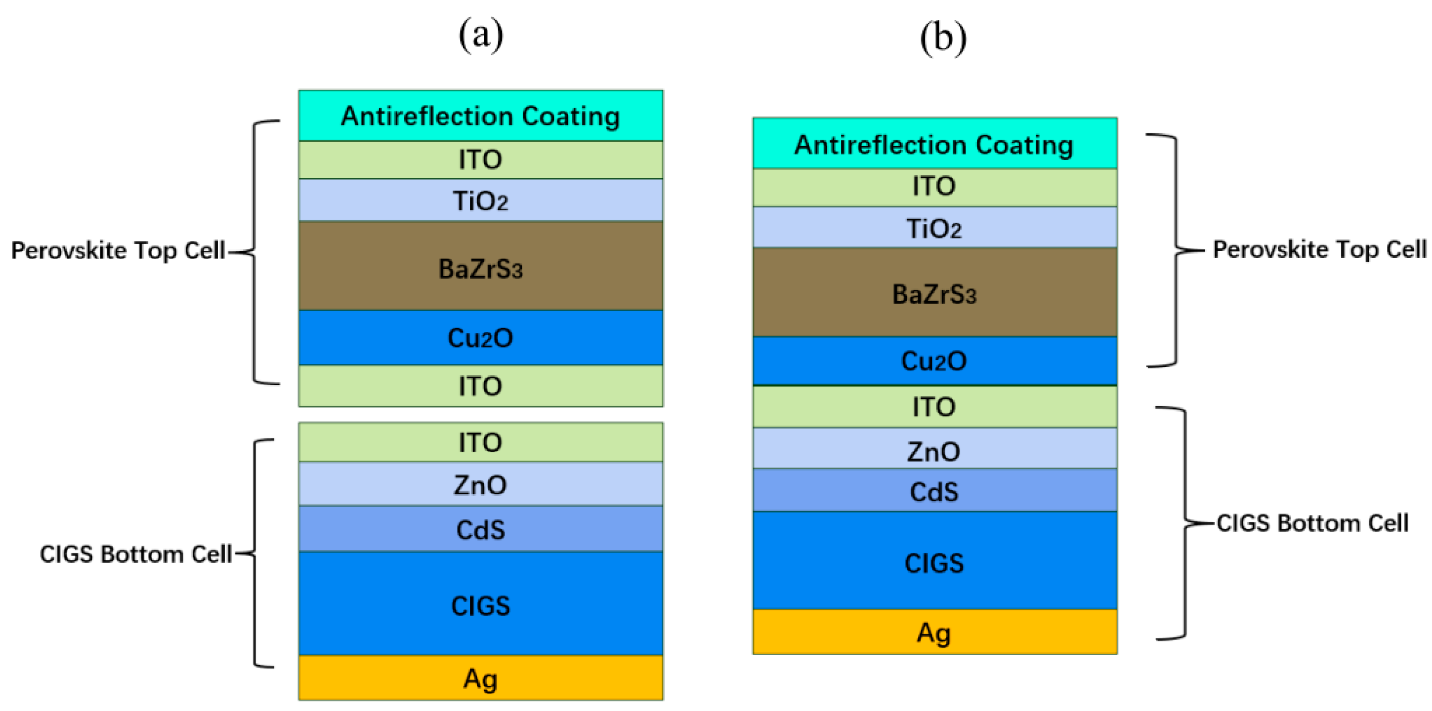
Figure 1: BaZrS3/GIGS tandem device (a) 4-T structure (b) 2-T structure.
Table 1: Materials parameters for BaZrS3 and CIGS solar cells.
| Parameter | TiO2 | BaZrS3 | Cu2O | ZnO | CdS | CIGS |
|---|---|---|---|---|---|---|
| Eg (eV) | 3.2 | 1.78 | 2.2 | 3.3 | 2.4 | 1.18 |
| χ (eV) | 4.0 | 4.1 | 3.4 | 4.45 | 4.2 | 4.36 |
| εr | 9.0 | 9.6 | 7.5 | 9 | 10 | 13.6 |
| NC (cm−3) | 2.2 × 10¹⁸ | 2.2 × 10¹⁸ | 2.2 × 10¹⁹ | 2.2 × 10¹⁸ | 2.2 × 10¹⁸ | 2.2 × 10¹⁸ |
| NV (cm−3) | 1.8 × 10¹⁹ | 1.8 × 10¹⁹ | 1.0 × 10¹⁹ | 1.8 × 10¹⁹ | 1.8 × 10¹⁹ | 1.5 × 10¹⁹ |
| μn (cm2/V s) | 100 | 11.3 | 200 | 100 | 100 | 100 |
| μp (cm2/V s) | 25 | 5.58 | 8600 | 25 | 25 | 12.5 |
| ND (cm−3) | 1 × 10¹⁸ | 0 | 1 × 10¹⁸ | 1 × 10¹⁸ | 1 × 10¹⁸ | 0 |
| NA (cm−3) | 0 | 1 × 10¹⁵ | 0 | 0 | 0 | 1 × 10¹⁶ |
| NT (cm−3) | 1 × 10¹⁴ | 1 × 10¹⁴ | 1 × 10¹⁴ | 1 × 10¹⁴ | 1 × 10¹⁴ | 1 × 10¹⁴ |
3.1 Simulation and Optimization of 4-T BaZrS3/CIGS Tandem Devices
3.1.1 Absorber Thickness Optimization in Subcells
The overall efficiency of four-terminal tandem solar cells is primarily determined by the thickness of their constituent subcells. In this study, the thickness of the top BaZrS3 absorber layer was systematically varied from 100 nm to 1200 nm, while the thickness of the bottom CIGS subcell was held constant at 2.5 μm. The corresponding power conversion efficiencies obtained from simulation are presented in Fig. 2a. Increasing the thickness of the top absorber significantly enhances the efficiency of the top subcell, which saturates beyond 1000 nm. Conversely, the efficiency of the bottom subcell exhibits a gradual decline. Since the total efficiency of the 4-T tandem equals the sum of the individual subcell efficiencies, the overall device efficiency increases gradually until it also reaches saturation. The tandem device achieves peak performance at a BaZrS3 thickness of 1100 nm.
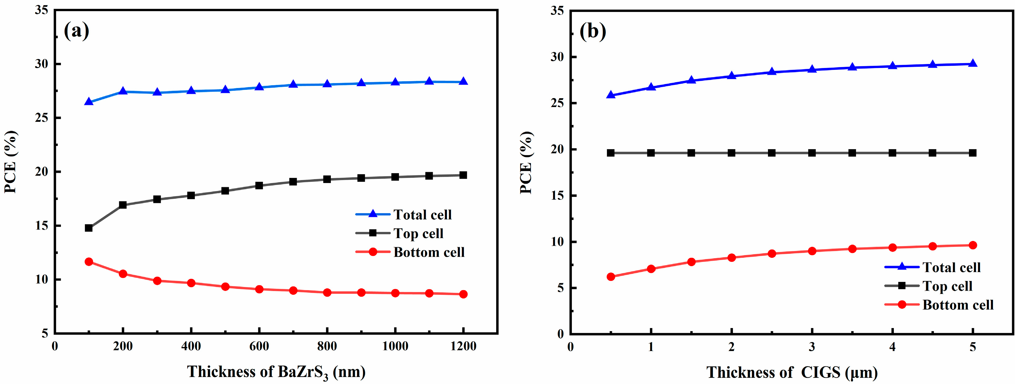
Figure 2: The PCE of subcells and 4-T tandem devices varies with the thickness of (a) BaZrS3 and (b) CIGS.
Consequently, the thickness of the top absorber was fixed at 1100 nm, while the thickness of the bottom CIGS absorber was systematically varied from 0.5 μm to 5 μm. The corresponding power conversion efficiency is presented in Fig. 2b. As shown, the efficiency of the top cell remains largely unchanged with increasing CIGS thickness, whereas the efficiency of the bottom cell increases steadily. Since the tandem efficiency is largely determined by the bottom cell, the overall efficiency exhibits a corresponding continuous rise. The maximum efficiency of the four-terminal tandem device reaches 28.86%, achieved with a BaZrS3 absorber thickness of 1100 nm and a CIGS absorber thickness of 4.5 μm.
To further investigate the factors governing tandem device performance, simulations were performed to determine the Jsc and EQE of the individual subcells, as shown in Fig. 3a,b. The results indicate that as the absorber layer thickness increases, the variation in Jsc closely follows the trend in device efficiency, implying that the observed fluctuations in power conversion efficiency are primarily driven by changes in Jsc. Fig. 3c presents the EQE spectra with the bottom CIGS absorber thickness fixed at 2.5 μm and the top BaZr3 thickness set to 100 nm, 500 nm, and 1000 nm. The spectra reveal a partial spectral absorption overlap between the two subcells. In the tandem structure, absorption is allocated spectrally: the top cell covers the 300–730 nm range, while the bottom cell covers 400–1100 nm. Optimizing the BaZrS3 thickness and minimizing optical reflection are therefore critical for maximizing light harvesting. As the BaZrS3 layer thickens from 100 nm to 500 nm, absorption in the top cell increases significantly within the 400–700 nm region, whereas absorption in the bottom cell decreases. This suggests that a thicker top absorber not only reduces infrared reflection but also attenuates the photon flux reaching the CIGS bottom cell, resulting in a continuous decline in its Jsc. What is more important is that the optical interference effect in the multi-layer thin film structure modifies the light field distribution. Increasing the thickness of the top subcell alters the overall optical cavity of the tandem structure, leading to changes in the reflectivity and parasitic absorption at specific wavelengths (especially the absorption edge and near-infrared region), thereby affecting the light intensity reaching the CIGS layer. These combined optical effects result in a decrease in the Jsc of the CIGS bottom subcell, and thus a reduction in its PCE.
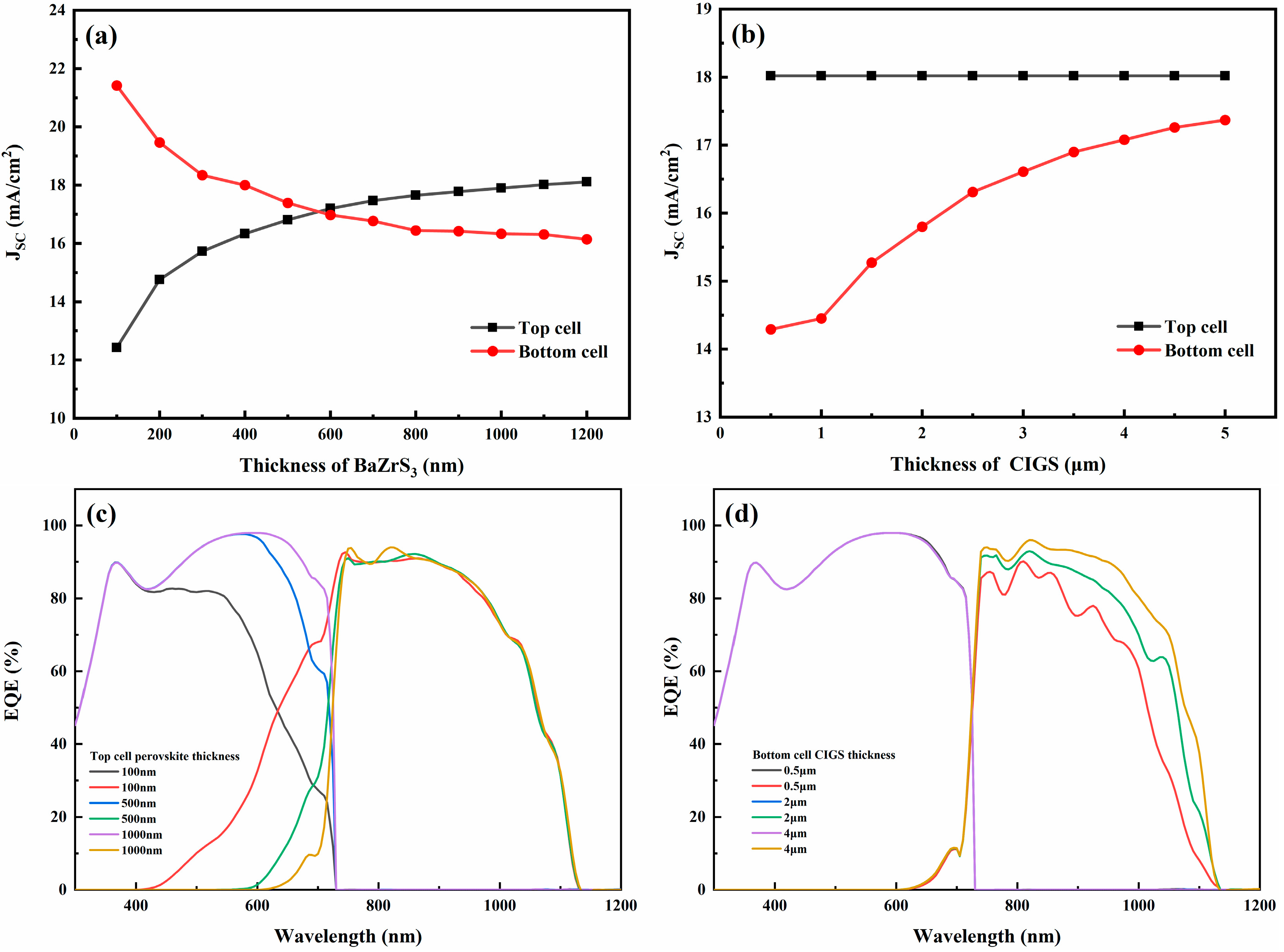
Figure 3: Effect of subcell absorber layer thickness variations in the 4-T tandem device on (a,b) Jsc and (c,d) EQE.
When the BaZrS3 thickness is increased further to 1000 nm, the absorption of the top cell in the short-wavelength region exhibits no substantial increase, with only a marginal enhancement observed between 600–700 nm. This suggests that photon absorption in the top cell has approached saturation. Meanwhile, incident radiation with wavelengths longer than 730 nm cannot be absorbed by the perovskite layer. After undergoing multiple internal reflections, this long-wavelength light reaches the bottom cell, where optical interference occurs between the reflected and incident light from adjacent regions. This interference is reflected as oscillatory features in the EQE curve of the bottom cell. Fig. 3d presents the EQE spectra with the top BaZrS3 absorber fixed at 1000 nm, while the thickness of the CIGS bottom cell was varied at 0.5 μm, 2 μm, and 4 μm. As the CIGS thickness increases, the EQE of the top cell remains nearly unchanged, whereas the bottom cell exhibits progressively stronger absorption across the 700–1100 nm spectral range. This trend in spectral response aligns well with the corresponding variation in Jsc shown in Fig. 3b. Additionally, due to optical interference effects, the EQE curve of the bottom cell displays characteristic oscillatory behavior.
The dependence of Voc on absorber thickness was further investigated; the results are shown in Fig. 4. As the BaZrS3 thickness increases, the Voc of the top cell decreases significantly due to the reduced splitting of electron and hole quasi-Fermi levels in the perovskite, whereas the Voc of the bottom cell remains nearly constant. Conversely, increasing the CIGS thickness has little effect on the top-cell Voc but leads to a continuous increase in the bottom-cell Voc. This rise is primarily attributed to enhanced photon absorption in the bottom cell, which boosts the photocurrent and consequently improves Voc through more efficient carrier collection.
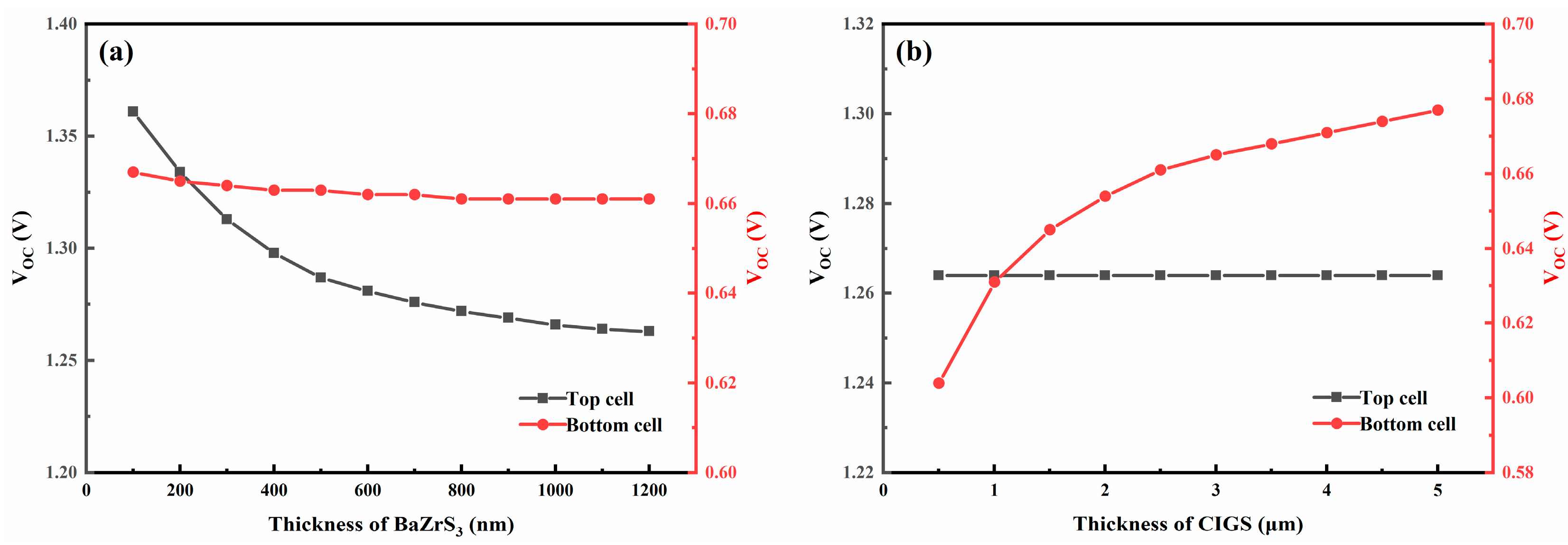
Figure 4: Variation of subcells Voc with the thickness of (a) BaZrS3 and (b) CIGS.
3.1.2 Analysis of Parasitic Absorption in Tandem Solar Cells
Parasitic absorption, along with optical reflection losses, constitutes a significant efficiency-limiting factor in tandem solar cells. It occurs when incident photons are absorbed by the carrier transport layers (CTLs) instead of the intended photoactive absorbers, thereby reducing the useful photocurrent. Investigating and minimizing such parasitic losses in tandem device architectures is therefore essential. In this section, we systematically analyze the photon absorption profile within the device as a function of CTL thickness. By precisely controlling the thickness of each functional layer, an optimized optical design is achieved, which mitigates parasitic absorption while maximizing useful photon utilization.
Photon absorption rates were simulated with TiO2/Cu2O/ZnO/CdS layer thicknesses set to 200 nm/80 nm/80 nm/50 nm, respectively. As shown in Fig. 5a, significant parasitic absorption occurs in the TiO2 layer within the 300–500 nm spectral range, substantially limiting the photon-harvesting capability of the top perovskite absorber. In addition to its charge-transport function, the TiO2 layer also contributes to minor parasitic absorption across the entire wavelength range. Meanwhile, ZnO—the electron transport layer in the bottom cell—exhibits considerable parasitic absorption in the 600–1000 nm infrared region. This undesired absorption further constrains the collection of long-wavelength photons by the CIGS bottom subcell, thereby reducing overall spectral utilization. In comparison, parasitic absorption from the Cu2O and CdS layers is negligible at these thicknesses. When the TiO2 thickness is reduced to 50 nm and the ZnO thickness is increased to 300 nm, a noticeable decrease in TiO2 parasitic absorption is observed within the 400–700 nm range, leading to improved photon absorption in the top cell. However, the increased ZnO thickness enhances its parasitic absorption in the long-wavelength region (700–1000 nm), which consequently attenuates photon harvesting in the bottom cell. In contrast, the CdS buffer layer contributes only minimal photon absorption loss.
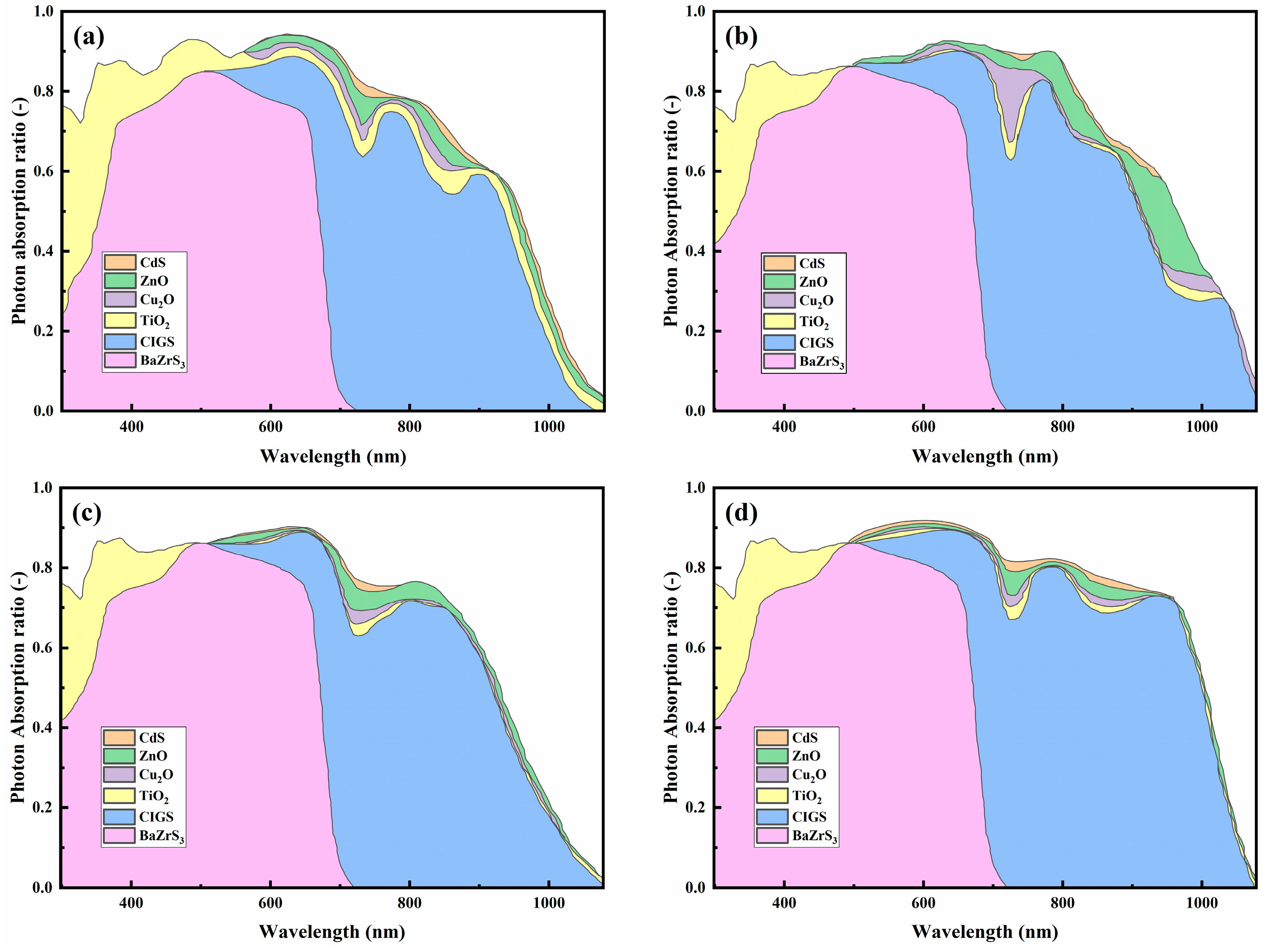
Figure 5: Photon absorption rate in the four-terminal BaZrS3/CIGS tandem solar device with TiO2/Cu2-O/ZnO/CdS CTLs thicknesses of (a) 200 nm/80 nm/40 nm/150 nm, (b) 50 nm/200 nm/300 nm/150 nm, (c) 50 nm/80 nm/40 nm/150 nm, and (d) 50 nm/80 nm/40 nm/60 nm.
As shown in Fig. 5d, when all carrier transport layers are reduced to optimized thicknesses, parasitic absorption is effectively suppressed, and optical absorption in both the top and bottom cells is significantly enhanced. Through careful selection of CTL thicknesses, parasitic losses in the tandem device can be minimized, while carrier transport and charge separation efficiency are improved, leading to an overall enhancement in device performance.
In this work, the initial thicknesses of the carrier transport layers were set to 50 nm. Following the optimization procedure outlined in this section, the thicknesses of TiO2/Cu2O/ZnO/CdS were adjusted to 50 nm/80 nm/40 nm/60 nm, respectively. This optimization resulted in an increase in the efficiency of the 4-T tandem device from 28.86% to 29.09%.
3.1.3 Effect of CTLs Doping Concentration on Tandem Device
The doping concentration in the CTLs was systematically varied from 1015 cm−3 to 1021 cm−3 to explore its impact on the four-terminal tandem device’s performance. This analysis aimed to identify optimal doping profiles by simulating the consequent variations in the overall power conversion efficiency.
Fig. 6a indicates that the overall device efficiency increases with rising TiO2 doping concentration and stabilizes when the concentration reaches 1018 cm−3. Fig. 6b demonstrates that the device efficiency increases monotonically with Cu2O doping concentration, reaching its maximum at 1021 cm−3. In contrast, varying the doping concentration of ZnO, which serves as the window layer of the bottom cell, has negligible impact on device efficiency. This can be attributed to the fact that the interfacial matching between ZnO and the CdS buffer layer has already reached an optimal and stable state within this concentration range, and changes in doping concentration do not significantly alter carrier separation and transport efficiency. As the buffer layer of the bottom cell, CdS functions to alleviate lattice mismatch between the CIGS absorber and the window layer. It only impedes device efficiency, causing a slight decrease, at a doping concentration of 1017 cm−3.
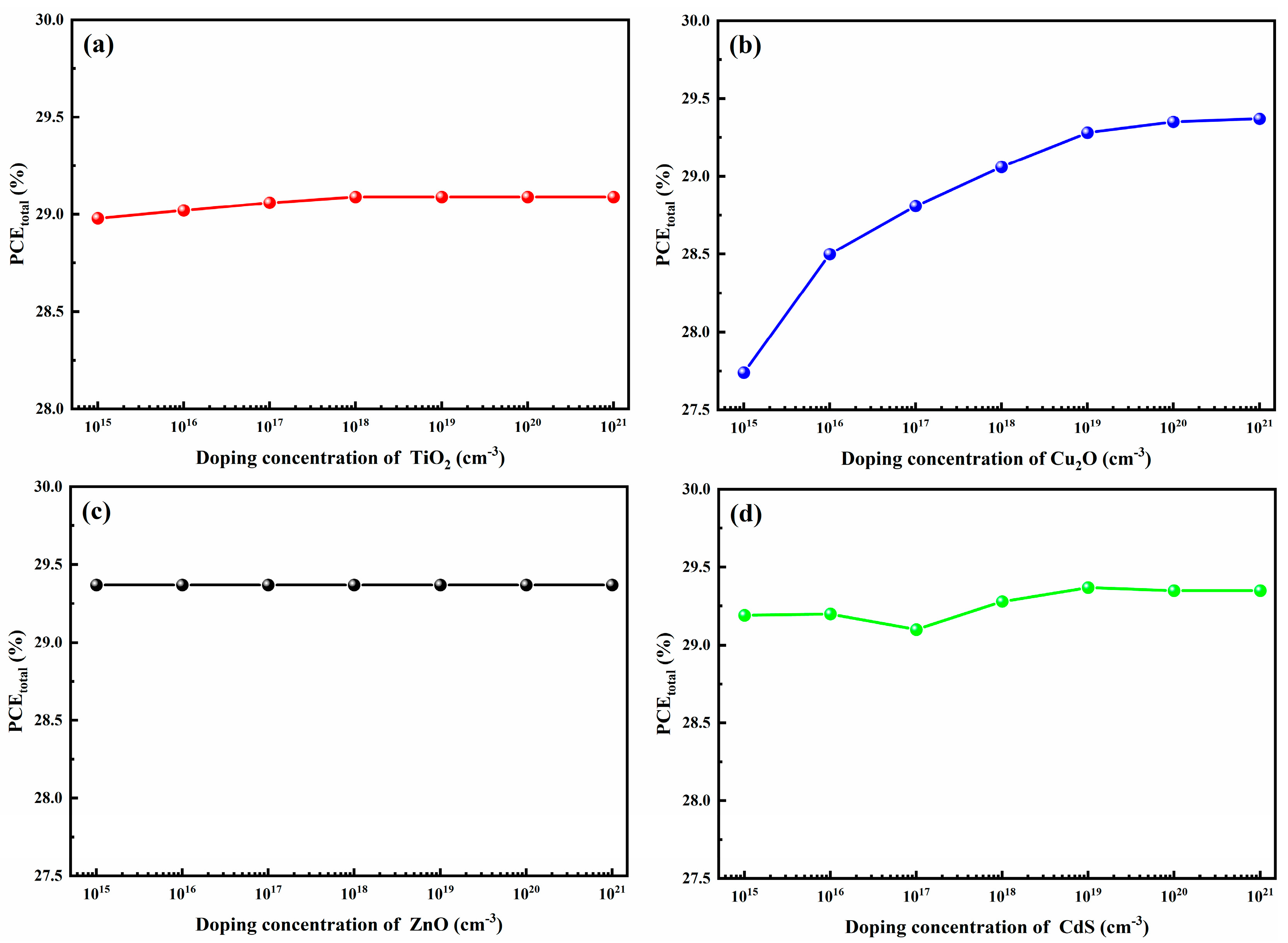
Figure 6: Effect of doping concentration in subcell CTLs on the total PCE of the tandem device: (a) TiO2, (b) Cu2O, (c) ZnO, (d) CdS.
In the initial simulation, the doping concentrations of the CTLs in both the top and bottom cells were set to 1018 cm−3. After the optimization described in this section, the total PCE of the 4-T tandem device improved from 29.09% to 29.37%.
To clearly assess the impact of doping concentration in the CTLs on device performance, all transport layers were initially doped at 1015 cm−3. The resulting performance parameters were then compared with those obtained under an optimized doping profile, as illustrated in Fig. 7. The corresponding comparative data are compiled in Table 2.
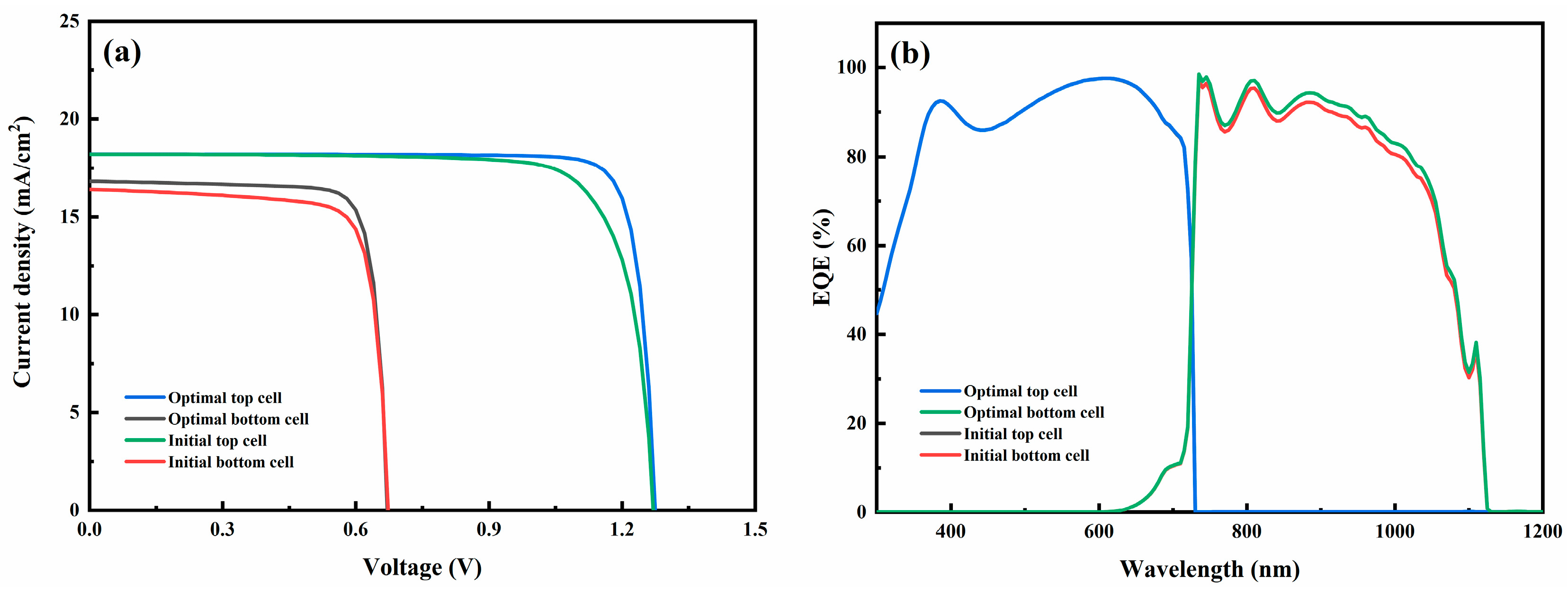
Figure 7: Under different CTLs doping concentrations: (a) J-V curves and (b) EQE of the 4-T tandem device.
Table 2: Comparison of photovoltaic parameters for the 4-T tandem device under varied doping concentrations in its CTLs.
| Doping Concentration of TiO2/Cu2O/ZnO/CdS (cm−3) | Cell | Jsc (mA/cm2) | Voc (V) | FF (%) | PCE (%) | Total PCE (%) |
|---|---|---|---|---|---|---|
| Initial 1015/1015/1015/1015 | Top | 18.21 | 1.271 | 79.80 | 18.45 | 27.14 |
| Bottom | 16.41 | 0.673 | 78.72 | 8.69 | ||
| Optimal 1018/1021/1019/1019 | Top | 18.22 | 1.274 | 86.76 | 20.13 | 29.37 |
| Bottom | 16.82 | 0.671 | 81.87 | 9.24 |
Table 2 reveals that altering the doping concentration in the top cell’s transport layers minimally affects its Jsc and Voc, but substantially enhances the FF. This gain in the top cell’s power conversion efficiency stems from improved carrier transport efficiency. By optimizing the doping concentrations of the TiO2 electron transport layer and the Cu2O hole transport layer to 1018 cm−3 and 1021 cm−3, we significantly enhanced their electrical conductivity and optimized the band offset with the BaZrS3 absorber layer. This reduction of the carrier extraction barrier at the interface is the core reason for the substantial improvement in the FF of the top subcell and its contribution to higher efficiency.
In contrast, optimizing the doping concentration in the transport layers of the bottom cell from its initial to the optimal level increases both Jsc and FF, despite a slight reduction in Voc. Fig. 7b shows that the EQE curve of the optimized bottom cell is elevated across the entire spectral range, indicating improved photon absorption and a higher yield of photogenerated carriers, which correspondingly raises Jsc. Furthermore, the increase in FF is attributed to the improved electrical conductivity and more efficient carrier transport in the optimized structure.
3.1.4 Study of the CIGS Absorber Layer
The doping concentration in the CIGS bottom absorber is a critical parameter governing the overall tandem efficiency. This section systematically examined the bottom-cell Jsc and Voc, the total device efficiency, and the corresponding energy-band diagrams across a range of doping levels. Considering that excessively high doping concentrations can introduce recombination centers that trap photogenerated carriers and severely hinder carrier transport efficiency, the doping concentration was varied from 1012 cm−3 to 1018 cm−3. The simulation results are presented in Fig. 8.
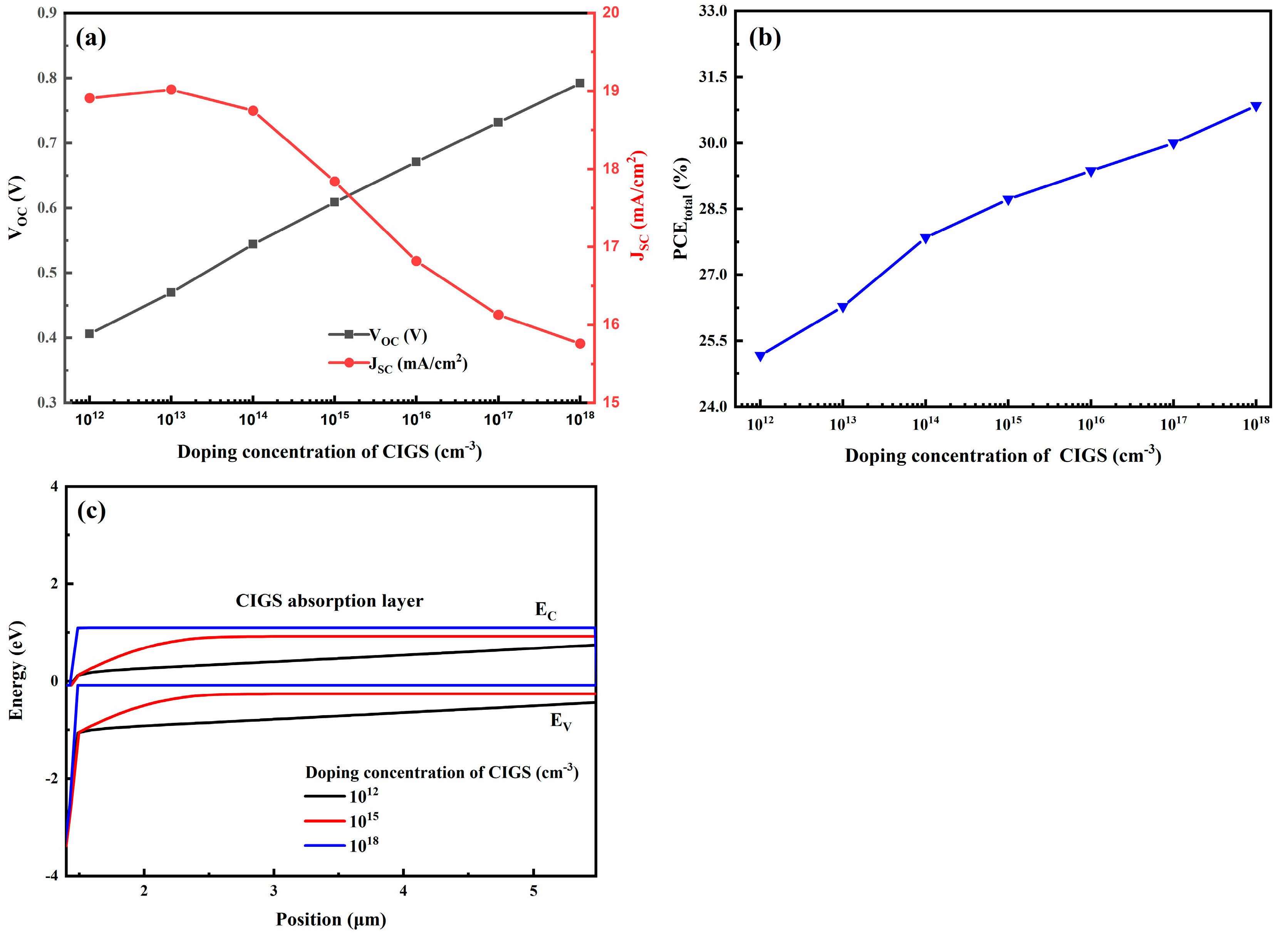
Figure 8: (a) Jsc and Voc of the bottom cell, (b) overall efficiency of the tandem device, and (c) energy band diagrams under different CIGS doping concentrations.
As shown in Fig. 8a, the dependence of Jsc and Voc on the doping concentration of the bottom CIGS layer reveals distinct trends. As the doping concentration increases, Jsc exhibits an initial slight increase followed by a rapid decline, while Voc shows continuous enhancement. At lower doping levels, a high probability of photogenerated carrier recombination coupled with limited collection efficiency constrains current output. A moderate increase in doping concentration establishes a more favorable carrier distribution, thereby reducing recombination losses and leading to the observed improvement in Jsc. However, with a further rise in doping concentration, a greater number of impurity-induced defect centers are introduced into the absorber. These defects promote non-radiative recombination, shorten the effective carrier lifetime, increase the overall recombination rate, and ultimately degrade the device current.
In Fig. 8c, the elevated carrier concentration induces more pronounced band bending within the CIGS layer, which promotes the extraction of photogenerated carriers at the interface. Consequently, the built-in electric field at the CIGS/CdS heterojunction is enhanced, while the depletion region narrows. Additionally, the increased photovoltage reduces the potential barrier at the p-n junction, enabling electrons from the CdS buffer layer to more readily transfer into the CIGS layer and recombine with holes. These combined effects contribute to the observed rise in Voc and the marked decline in Jsc. As summarized in Fig. 8b, the overall efficiency of the 4-T tandem device increases with doping concentration, reaching a maximum at 1 × 1018 cm−3. Accordingly, this concentration was selected as the optimal doping level for the bottom CIGS absorber. Following this optimization, the BaZrS3/CIGS 4-T tandem device achieved a final total power conversion efficiency of 30.85%.
3.1.5 Study of the ARC and the Top ITO Layer
The introduction of a suitable anti-reflection coating in tandem devices helps reduce reflection losses and enhance photon absorption, thereby improving both optical and electrical performance. For the 4-T configuration, the physical isolation of the subcells avoids chemical interactions at the interface, thereby reducing degradation caused by cross-contamination. The LiF anti-reflection coating not only enhances light absorption but also blocks the penetration of moisture and oxygen, providing additional protection for the top subcell. In this section, we systematically investigated the effect of LiF as an anti-reflection layer—selected for its low refractive index and excellent thermal stability—by varying its thickness and evaluating the resulting influence on the tandem device and its subcells. The simulation results are presented in Fig. 9.
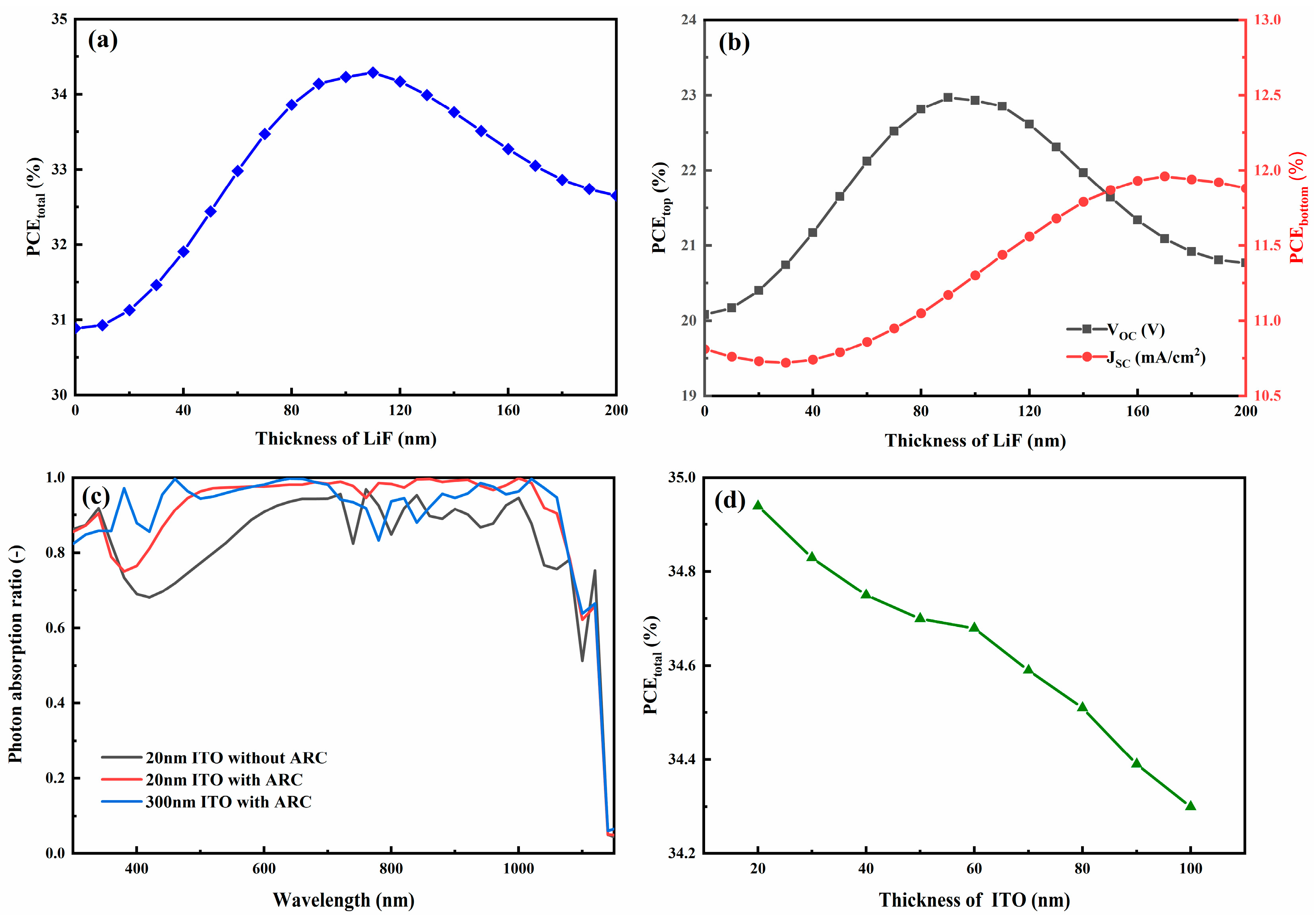
Figure 9: Variation of 4-T tandem devices with LiF thickness: (a) total PCE, (b) subcells PCE, (c) absorptivity under different conditions, and (d) variation of total PCE with top ITO electrode thickness.
As shown in Fig. 9a, the total PCE of the tandem device exhibits a non-monotonic dependence on the thickness of the LiF antireflection layer in the range of 0–200 nm, increasing initially before gradually declining, with an optimum thickness of 110 nm. Fig. 9b illustrates that the performance of both subcells improves as the LiF thickness increases up to a certain point. When the LiF thickness exceeds 90 nm, the efficiency of the top subcell decreases due to parasitic absorption within the LiF layer, whereas the efficiency of the bottom subcell continues to rise as a result of progressively reduced reflection losses.
Fig. 9c demonstrates that the introduction of an antireflection layer significantly enhances photon absorption across the entire spectral range. Furthermore, the performance of the tandem device is also influenced by the thickness of the top ITO electrode. Reducing the ITO thickness improves optical performance by increasing light transmission and minimizing reflection losses. However, as reported in prior studies, excessively thin ITO layers suffer from substantially reduced electrical conductivity, which can degrade overall device performance [30]. Fig. 9d illustrates the variation in device efficiency with ITO thickness. By balancing this optical-electrical trade-off, an ITO thickness of 50 nm was selected. Combined with the optimized antireflection layer, this adjustment increased the total PCE of the 4-T tandem solar cell from 30.85% to 34.7%.
3.2 Simulation and Optimisation of Two-Terminal BaZrS3/GIGS Tandem Devices
3.2.1 Study of Current Matching
Four-terminal tandem solar cells comprise two optically coupled yet electrically isolated subcells, whose individual power conversion efficiencies sum to yield the total device performance. The decoupled architecture of the 4-T design allows for independent structural optimization of each subcell, thus enabling higher overall efficiency. In contrast, two-terminal tandems feature subcells that are monolithically integrated via an intermediate recombination layer, forming a series-connected electrical circuit. In this configuration, the overall current is limited by the subcell generating the lower photocurrent. This imposes a strict current-matching requirement between subcells and represents a fundamental performance constraint. Nevertheless, two-terminal tandem devices benefit from lower parasitic absorption and reduced fabrication complexity compared to four-terminal designs, rendering them a more commercially viable pathway.
In the 2-T structure, the ITO tunneling recombination layer offers high optical transparency and chemical stability, which helps reduce charge accumulation at the interface and thereby lowers non-radiative recombination losses. However, the additional interface introduced represents a potential degradation site. Ion migration, diffusion, or interfacial reactions may occur under long-term operation or harsh environmental conditions. To achieve high performance in two-terminal tandem configurations, current matching is critically important. Building upon the previously optimized four-terminal tandem structure, we employed CIGS bottom cells with varying Ga contents to achieve current matching, aiming to identify the most compatible CIGS material structure for the BaZrS3 perovskite top cell.
The band gap of CIGS increases approximately linearly with the increase in Ga content, ranging from CuInSe2 (CIS, x = 0, Eg = 1.02 eV) to CuGaSe2 (CGS, x = 1, Eg = 1.68 eV) [31]. For tandems with wide-bandgap BaZrS3 top cells, a bottom cell with a moderate band gap is required to achieve effective current matching and voltage superposition. x = 0.3 (Eg = 1.18 eV) is a typical value for commercial high-efficiency single-junction CIGS solar cells, which achieves a good balance between Voc and Jsc, making it suitable as a benchmark for tandem research. x = 0.6 represents CIGS with a higher band gap (1.3–1.4 eV), aiming to explore the possibility of further improving the overall voltage potential of the tandem by enhancing the Voc of the bottom cell. Studies have shown that as the Ga content increases (x > 0.3), the formation energy of certain deep-level defects may decrease, leading to an increase in defect density [32]. These deep-level defects act as carrier recombination centers, reducing the minority carrier lifetime and thereby potentially impairing the device’s FF and Voc. As the Ga content in CI1−xGaxS (x = 0, 0.3, 0.6) increases, the bandgap widens from 1.02 eV to 1.37 eV [33]. The simulation results of the current matching study are presented in Fig. 10.
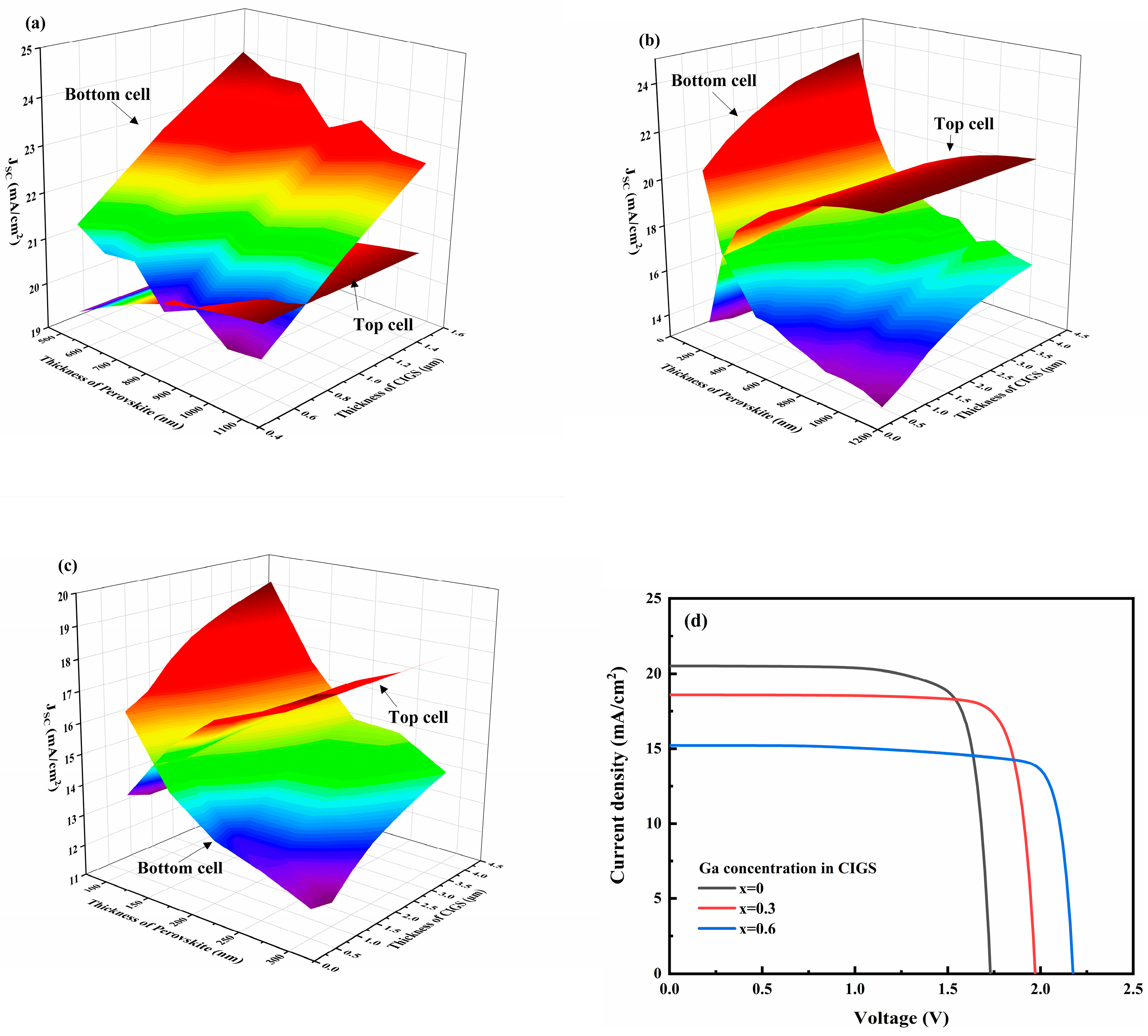
Figure 10: Current matching in two-terminal tandem devices using CIGS bottom cells with different Ga contents: (a) x = 0, (b) x = 0.3, (c) x = 0.6, and (d) the corresponding J-V characteristics under current-matched conditions.
Table 3 compiles the photovoltaic parameters of the two-terminal tandem devices under current-matched operation. The data show that raising the Ga content widens the bandgap of the CIGS bottom cell, which reduces the device’s Jsc but progressively increases its Voc. The optimal power conversion efficiency is achieved at a Ga content of 30%. By moderately incorporating Ga, Voc and FF are significantly enhanced at the expense of a partial decrease in Jsc, thus maximizing the power conversion efficiency. A maximum efficiency of 30.35% is achieved with the two-terminal tandem device employing a 400 nm BaZrS3 layer and a 4 μm CIGS absorber.
Table 3: Performance parameters of two-terminal tandem devices under current matching conditions with different Ga contents.
| CI1−xGxS | Jsc (mA/cm2) | Voc (V) | FF (%) | PCE (%) |
|---|---|---|---|---|
| x = 0 | 20.52 | 1.729 | 79.64 | 28.25 |
| x = 0.3 | 18.59 | 1.972 | 82.87 | 30.35 |
| x = 0.6 | 15.22 | 2.175 | 81.23 | 26.89 |
3.2.2 Study of CTLs Doping Concentration
Optimizing the doping concentration in CTLs can effectively improve the transport efficiency of photogenerated carriers within the device, thereby further enhancing the power conversion efficiency. By increasing the doping concentration from 1015 cm−3 to 1021 cm−3, we systematically investigated the performance variation of the BaZrS3/CIGS two-terminal tandem device under different doping levels in the CTLs. The simulation results, shown in Fig. 11, reveal trends largely consistent with those observed in the four-terminal tandem device under similar doping optimization. When the doping concentrations of the top-cell transport layers (TiO2 and Cu2O) were set to 1021 cm−3 and those of the bottom-cell transport layers (ZnO and CdS) to 1019 cm−3, the 2-T tandem device achieved a PCE of 31.5%, up from the initial 30.35%. Correspondingly, the device delivered Voc of 1.99 V, Jsc of 18.59 mA/cm2, and FF of 84.98%. In the 2-T tandem, achieving current matching relies not only on adjusting the CIGS bandgap via Ga content but also on the band alignment formed at the intermediate ITO tunneling junction between the top cell (ITO/Cu2O) and the bottom cell (ZnO/ITO). The optimized ITO layer and the doping configuration of the adjacent CTLs ensure the efficient recombination of electrons from the top cell with holes from the bottom cell at this interface, thereby enabling low-loss series current connection.
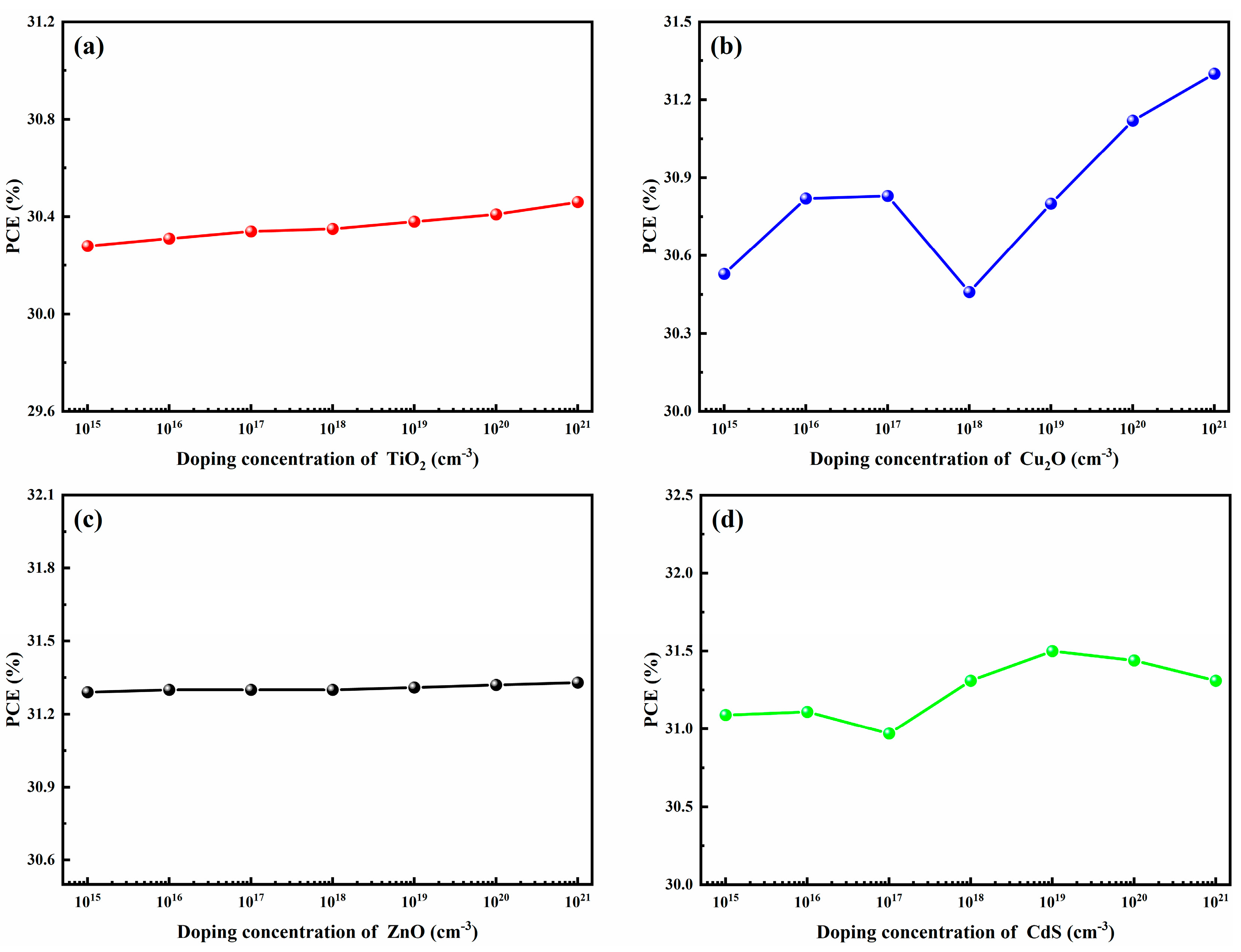
Figure 11: Effect of doping concentration in carrier transport layers on the PCE of the 2-T tandem device: (a) TiO2, (b) Cu2O, (c) ZnO, (d) CdS.
3.2.3 Study of CIGS Doping Concentration in Two-Terminal Device
The doping concentration in the CIGS bottom absorber is varied to examine its effect on the efficiency of two-terminal BaZrS3/CIGS tandem solar cells in this study. As illustrated in Fig. 12a, increasing the doping concentration in CIGS enhances the tandem device’s overall efficiency, which peaks at 32.65% when the doping level reaches 1018 cm−3. During this process, the device’s Jsc decreases while the Voc increases, a trend that aligns with the findings reported for four-terminal devices. Furthermore, Fig. 12b reveals that the two-terminal structure attains a higher photon absorption rate with lower parasitic losses compared to its four-terminal.
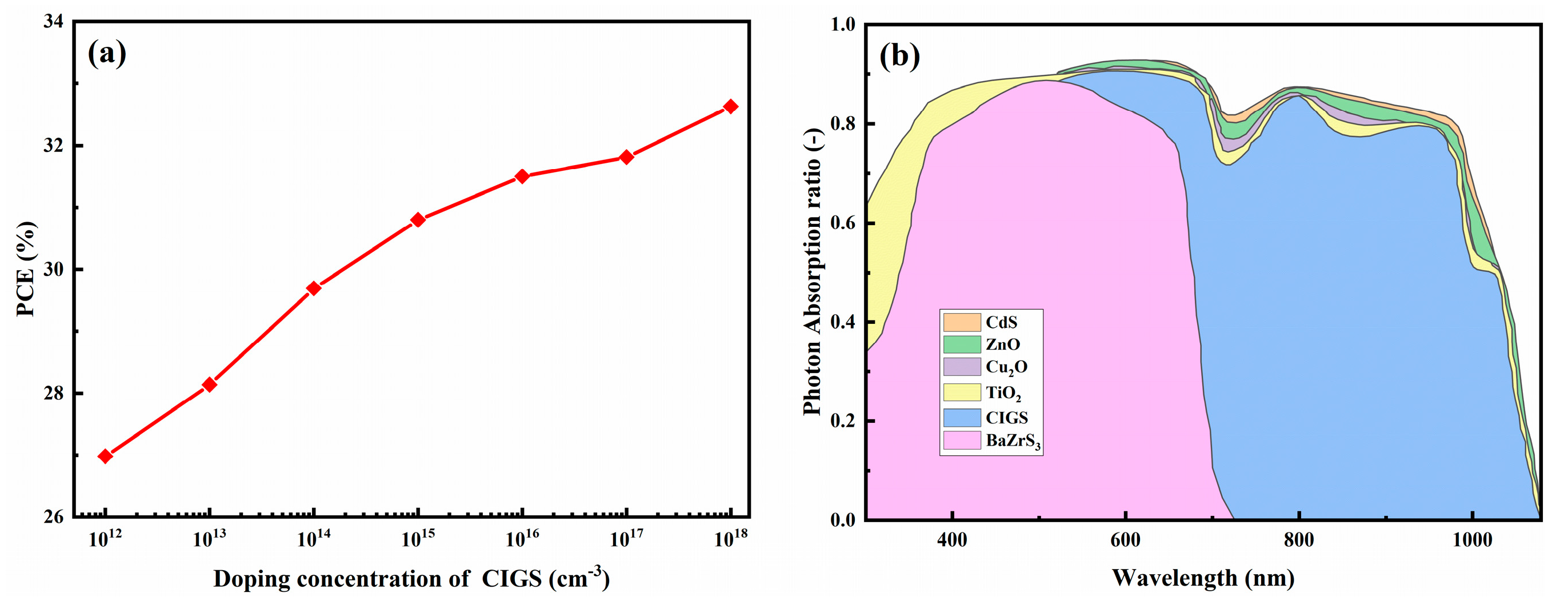
Figure 12: 2-T tandem device (a) variation PCE with CIGS doping concentration, (b) photon absorption rate.
In practical fabrication, the defect density within perovskite thin films significantly impacts the power conversion efficiency of tandem devices, as introduced defects act as recombination centers that capture charge carriers and increase recombination rates. In this study, we initially set the perovskite defect density to 1014 cm−3 and simulated its influence on tandem device performance across varying defect densities. The results are presented in Fig. 13. As the defect density in the BaZrS3 top absorber layer increases from 1014 cm−3 to 1017 cm−3, the Jsc of the two-terminal tandem device remains largely stable, while its Voc undergoes a progressive reduction. As the defect density reaches 1018 cm−3, FF drops markedly. The elevated trap-state density within the device promotes carrier recombination, which significantly compromises the overall power conversion efficiency. This is reflected in specific parameter degradations: the Voc of the two-terminal tandem cell decreases from 2.11 V to 1.79 V, and its FF plummets from 88.31% to 49.19%. Consequently, the device efficiency drops markedly from 32.65% to 13.31%.
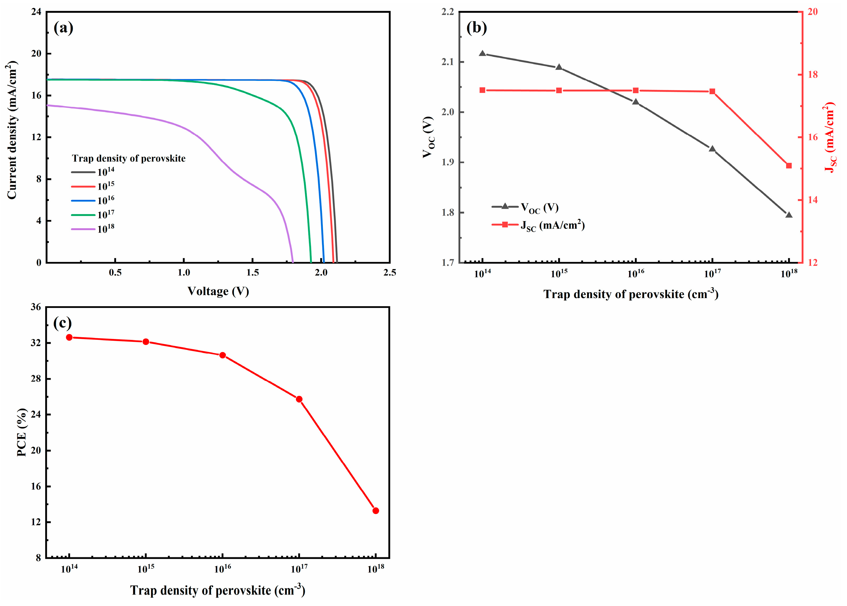
Figure 13: 2-T tandem device under varied perovskite defect densities: (a) J-V curves, (b) Voc and Jsc, (c) PCE.
The defect density within the perovskite layer has been demonstrated to significantly govern the efficiency of two-terminal tandem solar cells. Consequently, optimizing fabrication processes to enhance the quality of BaZrS3 perovskite films is imperative for mitigating efficiency losses. The structural optimization and current-matching strategies employed herein lead to a significant PCE improvement, as contextualized by the comparison of various PVK/CIGS devices presented in Table 4.
Table 4: Comparison of photovoltaic parameters for various PVK/CIGS devices.
| Working Mode | Jsc (mA/cm2) | Voc (V) | FF (%) | PCE (%) | Ref. |
|---|---|---|---|---|---|
| Experimental | 20.0 | 1.74 | 75.28 | 26.2 | [34] |
| 14.74 | 1.92 | 87.24 | 24.69 | [35] | |
| Simulation | 15.79 | 1.69 | 72.85 | 27.6 | [36] |
| 20.04 | 1.92 | 77 | 29.7 | [37] | |
| 17.59 | 2.29 | 85.69 | 34.52 | [38] | |
| 2-T Tandem cell | 17.52 | 2.11 | 88.31 | 32.65 | This work |
| 4-T Top cell | 20.56 | 1.277 | 86.58 | 22.72 | |
| 4-T Bottom cell | 17.56 | 0.796 | 85.73 | 11.98 | |
| 4-T Tandem cell | 34.7 | This work |
This study presents a simulation-based investigation and performance optimization of 4-T and 2-T BaZrS3/CIGS tandem solar cells. For the 4-T configuration, the power conversion efficiency was significantly improved through multiple optimization strategies: thickness optimization of the subcell absorber and carrier transport layers to reduce reflection and parasitic absorption losses; doping concentration optimization of the CTLs and the CIGS bottom absorber to enhance carrier transport efficiency; introduction of a LiF anti-reflection layer at the illumination side to enhance light harvesting; and systematic investigation of the top ITO electrode thickness. The integration of these optimization strategies ultimately produced a four-terminal BaZrS3/CIGS tandem solar cells exhibiting a champion PCE of 34.7%.
For the 2-T tandem device, building upon the optimized four-terminal structure, current matching was achieved using CIGS bottom cells with three different Ga compositions paired with the BaZrS3 top cell. The results indicate that the device with 30% Ga content in CIGS yielded the optimal efficiency of 30.35%. Further efficiency gains were realized through co-optimization of doping concentrations in the carrier transport layers and the CIGS bottom absorber, combined with an investigation into the effect of defect density in the BaZrS3 layer. These efforts culminated in a fully optimized 2-T BaZrS3/CIGS tandem device with a champion PCE of 32.65%. Future work will focus on the experimental fabrication of high-quality BaZrS3 thin films and their integration with CIGS solar cells, aiming to validate the structural design and performance predictions proposed by this simulation study.
Acknowledgement:
Funding Statement: The authors received no specific funding for this study.
Author Contributions: The authors confirm contribution to the paper as follows: study conception and design: Jun Zhang, Jiren Yuan; data collection: Jun Zhang, Wangjian Fu; analysis and interpretation of results: Jun Zhang, Jiren Yuan; draft manuscript preparation: Jun Zhang, Jiayi Song, Wangjian Fu, Jiren Yuan. All authors reviewed and approved the final version of the manuscript.
Availability of Data and Materials: Data available on request from the authors.
Ethics Approval: Not applicable.
Conflicts of Interest: The authors declare no conflicts of interest.
References
1. Burschka J , Pellet N , Moon SJ , Humphry-Baker R , Gao P , Nazeeruddin MK , et al. Sequential deposition as a route to high-performance perovskite-sensitized solar cells. Nature. 2013; 499( 7458): 316– 9. doi:10.1038/nature12340. [Google Scholar] [CrossRef]
2. Zeng Q , Zhang X , Feng X , Lu S , Chen Z , Yong X , et al. Polymer-passivated inorganic cesium lead mixed-halide perovskites for stable and efficient solar cells with high open-circuit voltage over 1.3 V. Adv Mater. 2018; 30( 9): 1705393. doi:10.1002/adma.201705393. [Google Scholar] [CrossRef]
3. Zhang B , Su J , Guo X , Zhou L , Lin Z , Feng L , et al. NiO/Perovskite heterojunction contact engineering for highly efficient and stable perovskite solar cells. Adv Sci. 2020; 7( 11): 1903044. doi:10.1002/advs.201903044. [Google Scholar] [CrossRef]
4. Chang J , Zhu H , Li B , Isikgor FH , Hao Y , Xu Q , et al. Boosting the performance of planar heterojunction perovskite solar cell by controlling the precursor purity of perovskite materials. J Mater Chem A. 2016; 4( 3): 887– 93. doi:10.1039/C5TA08398B. [Google Scholar] [CrossRef]
5. Chang J , Lin Z , Zhu H , Isikgor FH , Xu Q-H , Zhang C , et al. Enhancing the photovoltaic performance of planar heterojunction perovskite solar cells by doping the perovskite layer with alkali metal ions. J Mater Chem A. 2016; 4( 42): 16546– 52. doi:10.1039/C6TA06851K. [Google Scholar] [CrossRef]
6. Xiong Z , Zhang Q , Cai K , Zhou H , Song Q , Han Z , et al. Homogenized chlorine distribution for >27% power conversion efficiency in perovskite solar cells. Science. 2025; 390( 6773): 638– 42. doi:10.1126/science.adw8780. [Google Scholar] [CrossRef]
7. Sun YY , Agiorgousis ML , Zhang P , Zhang S . Chalcogenide perovskites for photovoltaics. Nano Lett. 2015; 15( 1): 581– 5. doi:10.1021/nl504046x. [Google Scholar] [CrossRef]
8. Sharma S , Ward ZD , Bhimani K , Sharma M , Quinton J , Rhone TD , et al. Machine Learning-Aided Band Gap Engineering of BaZrS(3) Chalcogenide Perovskite. ACS Appl Mater Interfaces. 2023; 15( 15): 18962– 72. doi:10.1021/acsami.3c00618. [Google Scholar] [CrossRef]
9. Wei X , Hui H , Zhao C , Deng C , Han M , Yu Z , et al. Realization of BaZrS3 chalcogenide perovskite thin films for optoelectronics. Nano Energy. 2020; 68: 104317. doi:10.1016/j.nanoen.2019.104317. [Google Scholar] [CrossRef]
10. Barman B , Ingole S . Analysis of Si back-contact for chalcogenide perovskite solar cells based on BaZrS3 using SCAPS-1D. Adv Theory Simul. 2023; 6( 7): 2200820. doi:10.1002/adts.202200820. [Google Scholar] [CrossRef]
11. Brinkmann KO , Wang P , Lang F , Li W , Guo X , Zimmermann F , et al. Perovskite–organic tandem solar cells. Nat Rev Mater. 2024; 9( 3): 202– 17. doi:10.1038/s41578-023-00642-1. [Google Scholar] [CrossRef]
12. Fang Z , Zeng Q , Zuo C , Zhang L , Xiao H , Cheng M , et al. Perovskite-based tandem solar cells. Sci Bull. 2021; 66( 6): 621– 36. doi:10.1016/j.scib.2020.11.006. [Google Scholar] [CrossRef]
13. Zhang Z , Li Z , Meng L , Lien SY , Gao P . Perovskite-based tandem solar cells: get the most out of the sun. Adv Funct Mater. 2020; 30( 38): 2001904. doi:10.1002/adfm.202001904. [Google Scholar] [CrossRef]
14. Bailie CD , Christoforo MG , Mailoa JP , Bowring AR , Unger EL , Nguyen WH , et al. Semi-transparent perovskite solar cells for tandems with silicon and CIGS. Energy Environ Sci. 2015; 8( 3): 956– 63. doi:10.1039/C4EE03322A. [Google Scholar] [CrossRef]
15. Han Q , Hsieh YT , Meng L , Wu JL , Sun P , Yao EP , et al. High-performance perovskite/Cu(In,Ga)Se(2) monolithic tandem solar cells. Science. 2018; 361( 6405): 904– 8. doi:10.1126/science.aat5055. [Google Scholar] [CrossRef]
16. García Cerrillo J , Distler A , Matteocci F , Forberich K , Wagner M , Basu R , et al. Matching the photocurrent of 2-terminal mechanically-stacked perovskite/organic tandem solar modules by varying the cell width. Solar RRL. 2023; 8( 3): 2300767. doi:10.1002/solr.202300767. [Google Scholar] [CrossRef]
17. McMeekin DP , Sadoughi G , Rehman W , Eperon GE , Saliba M , Horantner MT , et al. A mixed-cation lead mixed-halide perovskite absorber for tandem solar cells. Science. 2016; 351( 6269): 151– 5. doi:10.1126/science.aad5845. [Google Scholar] [CrossRef]
18. Loper P , Moon SJ , de Nicolas SM , Niesen B , Ledinsky M , Nicolay S , et al. Organic-inorganic halide perovskite/crystalline silicon four-terminal tandem solar cells. Phys Chem Chem Phys. 2015; 17( 3): 1619– 29. doi:10.1039/C4CP03788J. [Google Scholar] [CrossRef]
19. Jošt M , Köhnen E , Al-Ashouri A , Bertram T , Tomšič Š , Magomedov A , et al. Perovskite/CIGS tandem solar cells: from certified 24.2% toward 30% and beyond. ACS Energy Lett. 2022; 7( 4): 1298– 307. doi:10.1021/acsenergylett.2c00274. [Google Scholar] [CrossRef]
20. Liu M , Johnston MB , Snaith HJ . Efficient planar heterojunction perovskite solar cells by vapour deposition. Nature. 2013; 501( 7467): 395– 8. doi:10.1038/nature12509. [Google Scholar] [CrossRef]
21. Kumar A , Singh S , Mohammed MKA , Shalan AE . Computational modelling of two terminal CIGS/Perovskite tandem solar cells with power conversion efficiency of 23.1%. Eur J Inorg Chem. 2021; 2021( 47): 4959– 69. doi:10.1002/ejic.202100214. [Google Scholar] [CrossRef]
22. Khantar SA , Bendenia C , Bendenia S , Merad-Dib H , Moulebhar S , Merabet S . Silvaco simulation of single and bilayer Cs2PtI6 and CsPbI3 perovskite solar cells. Phys Scr. 2025; 100( 7): 076103. doi:10.1088/1402-4896/adedcf. [Google Scholar] [CrossRef]
23. Hossain MK , Bhattarai S , Arnab AA , Mohammed MKA , Pandey R , Ali MH , et al. Harnessing the potential of CsPbBr(3)-based perovskite solar cells using efficient charge transport materials and global optimization. RSC Adv. 2023; 13( 30): 21044– 62. doi:10.1039/D3RA02485G. [Google Scholar] [CrossRef]
24. Kumar M , Singh A , Gill D , Bhattacharya S . Optoelectronic properties of chalcogenide perovskites by many-body perturbation theory. J Phys Chem Lett. 2021; 12( 22): 5301– 7. doi:10.1021/acs.jpclett.1c01034. [Google Scholar] [CrossRef]
25. Vincent Mercy EN , Srinivasan D , Marasamy L . Emerging BaZrS3 and Ba(Zr,Ti)S3 chalcogenide perovskite solar cells: A numerical approach toward device engineering and unlocking efficiency. ACS Omega. 2024; 9( 4): 4359– 76. doi:10.1021/acsomega.3c06627. [Google Scholar] [CrossRef]
26. Su Q , Zuo C , Liu M , Tai X . A review on Cu2O-based composites in photocatalysis: synthesis, modification, and applications. Molecules. 2023; 28( 14): 5576. doi:10.3390/molecules28145576. [Google Scholar] [CrossRef]
27. Yu MJ , Yuan JR , Deng XH . Simulation study on lead-free double Cs2AgBiBr6/GaAs tandem solar cells. J Ovonic Res. 2025; 21( 1): 1– 18. [Google Scholar]
28. Liu SH , Yuan JR , Wu Y , Deng XH , Yu QM . Numerical simulation of Sb2Se3-based solar cells. Chalcogenide Lett. 2024; 21( 3): 229– 41. doi:10.15251/CL.2024.213.229. [Google Scholar] [CrossRef]
29. Liu W , Li H , Qiao B , Zhao S , Xu Z , Song D . Highly efficient CIGS solar cells based on a new CIGS bandgap gradient design characterized by numerical simulation. Solar Energy. 2022; 233: 337– 44. doi:10.1016/j.solener.2022.01.054. [Google Scholar] [CrossRef]
30. Consonni V , Rey G , Roussel H , Doisneau B , Blanquet E , Bellet D . Preferential orientation of fluorine-doped SnO2 thin films: The effects of growth temperature. Acta Mater. 2013; 61( 1): 22– 31. doi:10.1016/j.actamat.2012.09.006. [Google Scholar] [CrossRef]
31. Hanna G , Jasenek A , Rau U , Schock HW . Influence of the Ga-content on the bulk defect densities of Cu(In,Ga)Se2. Thin Solid Films. 2001; 387( 1–2): 71. doi:10.1016/S0040-6090(00)01710-7. [Google Scholar] [CrossRef]
32. Boubakeur M , Aissat A , Ben Arbia M , Maaref H , Vilcot JP . Enhancement of the efficiency of ultra-thin CIGS/Si structure for solar cell applications. Superlattices Microstruct. 2020; 138: 106377. doi:10.1016/j.spmi.2019.106377. [Google Scholar] [CrossRef]
33. Chen S , Walsh A , Yang J-H , Gong XG , Sun L , Yang P-X , et al. Compositional dependence of structural and electronic properties of Cu2ZnSn(S,Se)4 alloys for thin film solar cells. Physical Review B. 2011; 83( 12): 125201. doi:10.1103/PhysRevB.83.125201. [Google Scholar] [CrossRef]
34. Nakamura M , Lin CC , Nishiyama C , Tada K , Bessho T , Segawa H . Semi-transparent perovskite solar cells for four-terminal perovskite/CIGS tandem solar cells. ACS Appl Energy Mater. 2022; 5( 7): 8103– 11. doi:10.1021/acsaem.2c00620. [Google Scholar] [CrossRef]
35. Saeed A , Salah M , Zekry A , Mousa M , Shaker A , Abouelatta M , et al. Investigation of high-efficiency and stable carbon-perovskite/silicon and carbon-perovskite/CIGS-GeTe tandem solar cells. Energies. 2023; 16( 4): 1676. doi:10.3390/en16041676. [Google Scholar] [CrossRef]
36. Kumar A , Saurabh SD , Sharma H . Perovskite-CIGS materials based tandem solar cell with an increased efficiency of 27.5%. Mater Today Proc. 2021; 45: 5047– 51. doi:10.1016/j.matpr.2021.01.565. [Google Scholar] [CrossRef]
37. Shrivastav N , Kashyap S , Madan J , Al-Mousoi AK , Mohammed MKA , Hossain MK , et al. Perovskite-CIGS monolithic tandem solar cells with 29.7% efficiency: a numerical study. Energy Fuels. 2023; 37( 4): 3083– 90. doi:10.1021/acs.energyfuels.2c03973. [Google Scholar] [CrossRef]
38. Singh YK , Dwivedi DK , Lohia P , Pandey R , Madan J , Agarwal S , et al. Current matching and filtered spectrum analysis of wide-bandgap/narrow-bandgap perovskite/CIGS tandem solar cells: a numerical study of 34.52% efficiency potential. J Phys Chem Solids. 2025; 196: 112300. doi:10.1016/j.jpcs.2024.112300. [Google Scholar] [CrossRef]
Cite This Article
 Copyright © 2026 The Author(s). Published by Tech Science Press.
This work is licensed under a Creative Commons Attribution 4.0 International License , which permits unrestricted use, distribution, and reproduction in any medium, provided the original work is properly cited.
 Downloads
 Citation Tools