
 Submit a Paper
 Propose a Special lssue
 Open Access
ARTICLE

Attempting Doping Activation via Rapid Thermal Annealing in As-Doped Polycrystalline CdSeTe Solar Cells
1 College of Materials Science and Engineering, Sichuan University, Chengdu, China
2 Engineering Research Center of Alternative Energy Materials & Devices, Ministry of Education, Chengdu, China
3 Institute of New Energy and Low-carbon Technology, Sichuan University, Chengdu, China
* Corresponding Author: Jingquan Zhang. Email:
Chalcogenide Letters 2026, 23(3), 4 https://doi.org/10.32604/cl.2026.079159
Received 15 January 2026; Accepted 02 March 2026; Issue published 03 April 2026
 View Full Text
 Download PDF
Abstract
Doping the absorber layer is a critical process for enhancing the performance of polycrystalline CdSeTe solar cells. Replacing traditional Cu doping with Group V dopants offers a pathway to fabricate devices with improved efficiency and stability. However, the dopant activation rate in polycrystalline structures remains low, typically only a few percent. While rapid thermal annealing (RTA) has been successfully employed to achieve high activation rates in single-crystal CdTe devices, its application to polycrystalline CdSeTe solar cells has been scarcely reported. In this study, we systematically applied multi-step annealing to investigate the dopant activation of in-situ As-doped polycrystalline CdSeTe devices. Our findings reveal that polycrystalline devices exhibit significantly lower thermal tolerance than their single-crystal counterparts, sustaining only short-duration annealing at 500°C. Furthermore, although Cl diffusion during RTA can degrade device performance, we observed that trace amounts of CdCl2 vapor can help stabilize device efficiency.Graphic Abstract
Keywords
Polycrystalline CdSeTe solar cells have established themselves as a mainstream technology in the thin-film photovoltaic market, benefiting from their low manufacturing cost, structural stability, long operational lifetime, and considerable power conversion efficiency. Notably, First Solar Inc. has achieved a certified efficiency of 23.1% [1]. For many years, Cu has been the conventional dopant for p-type doping in the absorber layer and back contact formation. Although Cu doping is a mature process that substantially enhances device performance [2,3,4], it also leads to long-term degradation due to the high diffusion coefficient of Cu [5,6]. Moreover, the carrier concentration in Cu-doped devices is generally limited to the order of 1014 cm−3, a consequence of self-compensation effects and grain boundary segregation [7]. The deep transition level of Cu further complicates efficient ionization and can promote carriers recombination, thereby compromising device performance.
In recent years, Group V dopants—such as N, P, As and Sb—have been identified as promising alternatives to Cu [8,9]. These elements exhibit superior doping stability, shallower transition levels, and the potential to achieve higher carrier concentrations [10]. Several studies have reported Group V-doped devices with efficiencies approaching or exceeding 20%, with arsenic (As) being the most commonly employed dopant in this category [11,12,13,14].
In successful cases of As doping in polycrystalline CdTe films, carrier concentrations can exceed 1016 cm−3, but the dopant activation rate remains low—typically only a few percent [12,15]. In contrast, single-crystal CdTe devices have demonstrated activation efficiencies exceeding 40% [16]. A key reason contributing to this high activation in single-crystal systems is their ability to endure higher annealing temperatures. Both experimental and simulation studies confirm that the activation rate of Group V dopants improves with increasing temperature during RTA [10]. However, in polycrystalline devices—which often involve CdCl2 treatment during annealing and possess distinct microstructures—excessively rapid CdCl2 diffusion at elevated temperatures can cause interfacial damage and over-treatment.
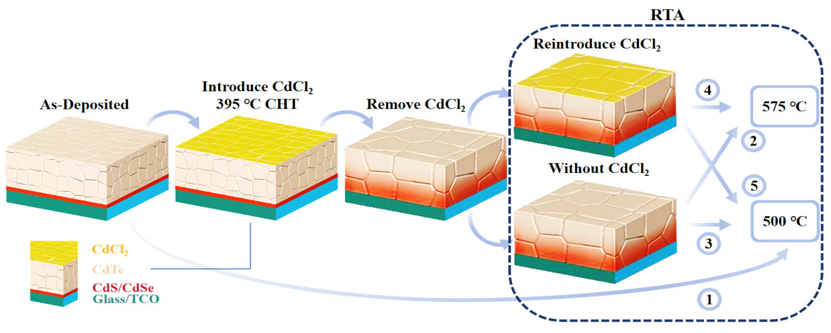
Recent research on single-crystal CdTe has shown that As dopant activation can be completed within a short duration, and such devices can withstand multiple annealing cycles, with the final activation rate determined primarily by the temperature of the last annealing step [17]. Inspired by these findings, we hypothesize that a multiple annealing strategy may also be applicable to polycrystalline devices. This approach aims to enhance dopant activation while mitigating the risks of over-treatment associated with rapid CdCl2 diffusion at high temperatures. To test this, we performed RTA at 500°C or 575°C following a standard chlorine heat treatment (CHT) at 395°C.
In this study, close-space sublimation (CSS) was employed to fabricate As-doped CdSeTe absorber layers, confirming the effectiveness of CSS for As incorporation. By systematically comparing devices subjected to CHT only, RTA only, and combined CHT + RTA treatments, we evaluate the role of RTA in activating As dopants and examine how annealing time and temperature influence device performance. We further demonstrate that a low-concentration CdCl2 atmosphere during RTA contributes to the stabilization for device performance.
Fig. 1 shows our device structure. MZO, CdS, and CdSe were sequentially deposited via magnetron sputtering onto fluorine-doped tin oxide glass (TecTM 12D). We found that devices incorporating a thin CdS layer demonstrate better reproducibility. The CdS layer is only 20 nm thick and interdiffuses with CdSe and CdTe during CHT. After CHT, the CdS layer no longer exists near the front interface, so it does not affect the blue response of the cell, as can be seen in the EQE measurements discussed later. The CdTe:As layer was deposited by CSS with a source temperature of 635°C and a substrate temperature of 570°C.
The CdTe:As source containing CdTe and 1 wt.% Cd3As2 was obtained by the rotating vertical Bridgman melt growth technique [18]. The devices then underwent optimized CHT: 0.05 mol/L CdCl2 aqueous solution was uniformly sprayed onto the deposited CdTe:As film surface using an ultrasonic sprayer for 90 s, followed by annealing at 395°C for 40 min. CdSe and CdTe interdiffuse during CHT to form the CdSeTe layer. Samples that have undergone CHT are considered baseline cells. Baseline cells were carefully cleaned to remove CdCl2 from the back surface. Note that rinsing with deionized water alone still leaves CdCl2 residue on the back surface; scrubbing with a brush is necessary. Subsequently, baseline cells underwent RTA in a tube furnace at high temperature of 500°C or 575°C for 3 to 10 min, with a fan used to accelerate cooling. To remove the oxide layer, improve contact resistivity, and clean surface contaminants, samples were etched in 0.2% Br-MeOH solution for 5 s, followed by sequential rinsing with methanol, ethanol, and deionized water. Finally, Au was evaporated as the back contact. For convenient measurement, the devices were segmented into small cells with an area of 0.24 cm2 via laser scribing, and In electrodes were soldered onto the surrounding FTO.
The average As concentration in the absorber layer was measured by inductively coupled plasma-mass spectrometer (ICP-MS). The absorber layer on the glass substrate was dissolved in dilute HNO3 solution and diluted to volume. The detection limit of ICP-MS reaches the ppt level, with a detection limit for As of 5 × 10⁻⁶ mg/L. The instrument had been calibrated before the test. The average As concentration in the absorber layer was calculated using the following formula:
The carrier concentration of the absorber layer was obtained from capacitance-voltage measurement (C-V) under dark conditions, at a frequency of 100 kHz, a step size of 5 mV, and a bias voltage ranging from −1 V to 1 V. C-V were performed using an Agilent 4156 semiconductor parameter analyzer. Light J-V measurements were performed under standard AM1.5 G illumination (100 mW/cm2) using a Sun 3000 solar simulator (ABET Technologies). Prior to measurement, the light intensity was precisely calibrated with a NIST-traceable GaAs reference cell. The external quantum efficiency (EQE) was characterized using a QEX10 measurements. Samples were immersed in liquid nitrogen for low-temperature brittle fracture, and the cross-sections were prepared after sputtering with gold. Scanning Electron Microscope (SEM) and Energy Dispersive Spectrometer (EDS) analyses were performed using a ZEISS GeminiSEM 300 with a magnification of 40k×.
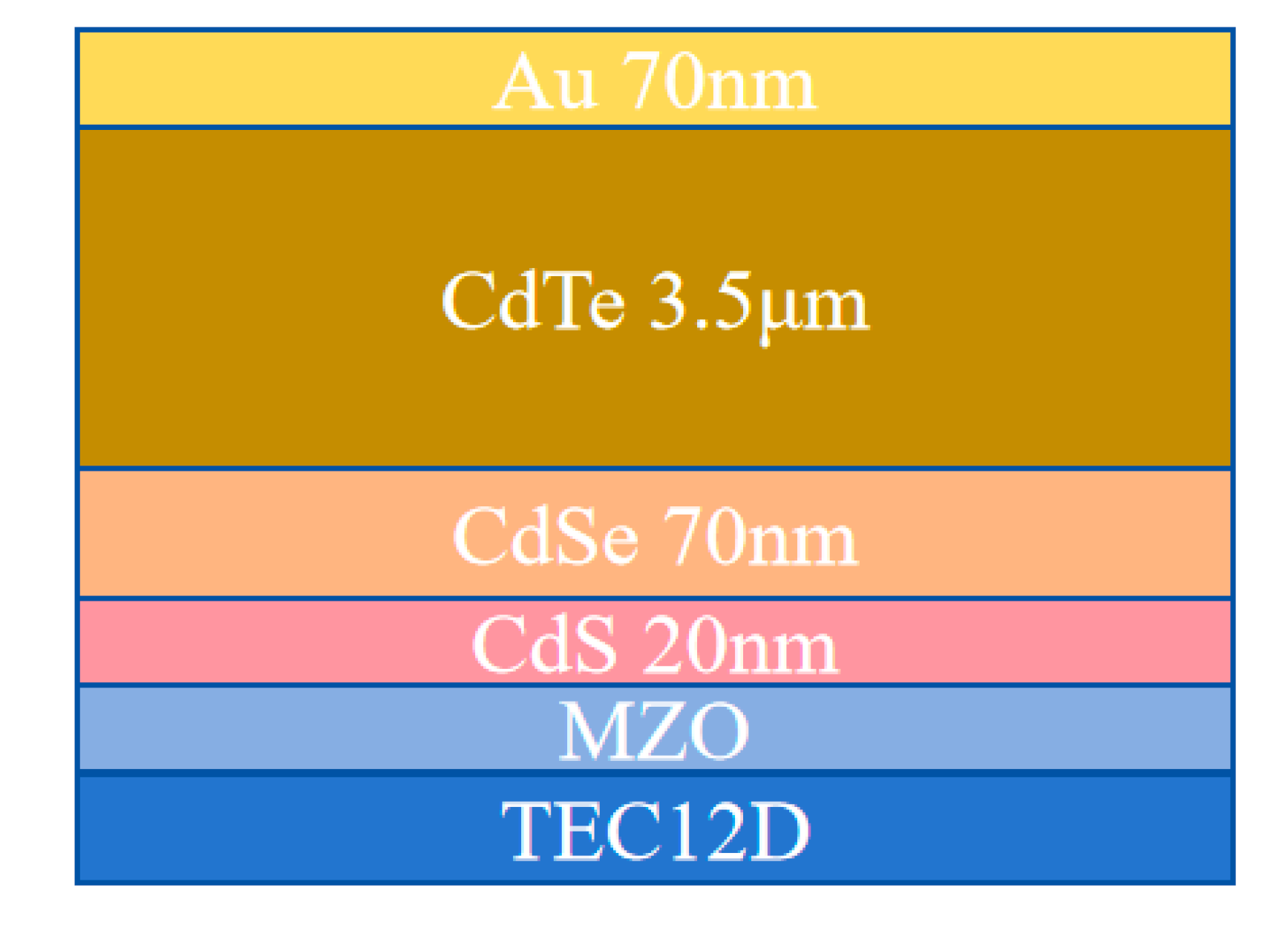
Figure 1: Schematic of the device structure.
3.1 Verification of CSS Doping Effectiveness
Table 1 shows the As concentration in the digestion solution and the film area and thickness. The total thickness is the sum of the thicknesses of multiple dissolved films. Since the CdTe:As layer is only a few micrometers thick, dissolving too few samples would affect the accuracy of the ICP-MS measurement. Substituting the values from Table 1 into Eq. (1), the As concentration in the CdTe:As layer is 4.18 × 1017 cm−3, which is commonly reported for CSS-fabricated CdSeTe:As or CdTe:As layers [19,20]. According to reported SIMS profiles of As, high concentrations of As segregate at the front interface, which is related to the oxidation of As [21,22]. The actual As concentration in the absorber layer should be less than 4.18 × 1017 cm−3. Fig. 2 shows the efficiency of doped and undoped baseline cells within similar batches, with performance parameters listed in Table 2. The performance of the doped device is significantly improved, especially in terms of Voc and FF. Improvement of hole concentration in the absorber layer can enhance the separation efficiency of photogenerated carriers, reduce non-radiative recombination, and increase Voc. Simultaneously, the increased carrier concentration improves the conductivity of the absorber layer, leading to a reduction in Rs and an increase in FF. As doping greatly improves device performance, demonstrating the effectiveness of in-situ As doping via CSS.
Table 1: Parameters of the CSS-deposited CdTe:As layer.
| V0 (mL) | C0 (ug/L) | S (cm2) | L (μm) | MAs | mAs (g) | CAs (cm−3) |
|---|---|---|---|---|---|---|
| 40 | 20 | 15.84 | 9.7 | 74.92 | 8 × 10⁻⁷ | 4.18 × 10¹⁷ |
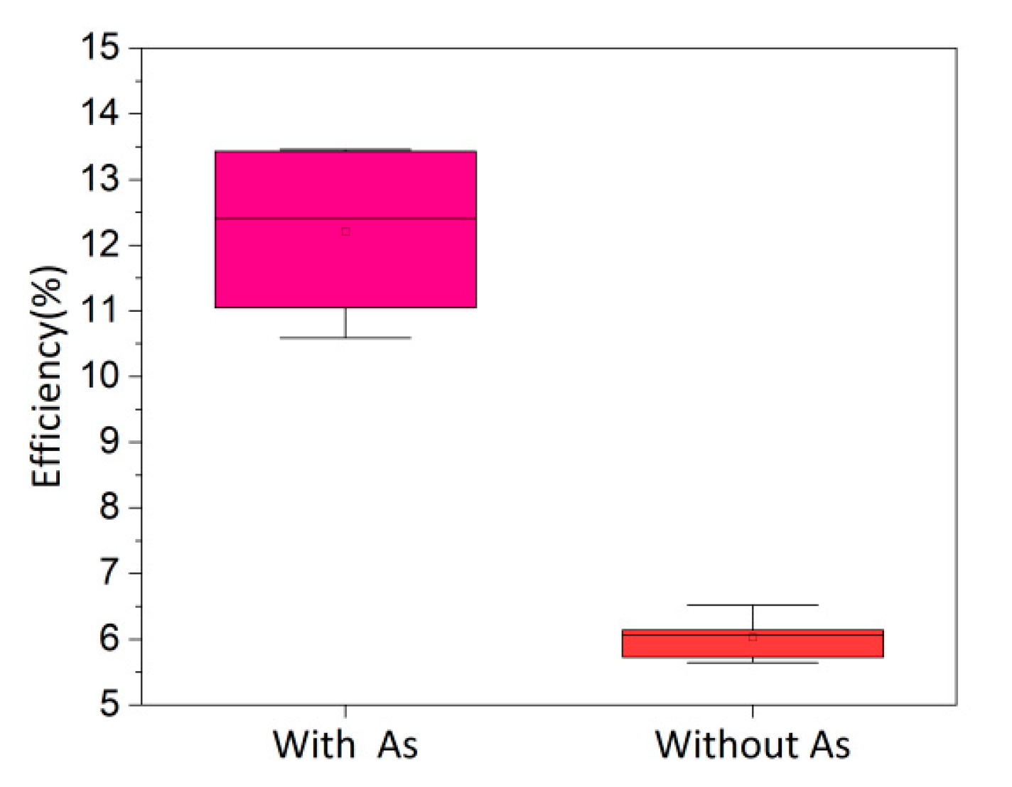
Figure 2: Efficiency of As-doped and undoped devices after CHT.
Table 2: Performance parameters from light J-V curves of As-doped and undoped devices after CHT.
| Eff (%) | Jsc (mA/cm2) | Voc (mV) | FF (%) | Rs (Ω·cm2) | Rsh (Ω·cm2) | |
|---|---|---|---|---|---|---|
| Without As | 6.52 | 25.92 | 537 | 46.83 | 9.41 | 157.78 |
| With As | 13.46 | 27.53 | 803 | 60.84 | 6.85 | 749.33 |
RTA is widely used for Group V dopant activation in single-crystal CdTe but is rarely applied to polycrystalline CdSeTe activation. Single-crystal CdTe has no grain boundaries, unlike polycrystalline CdSeTe, thereby obviating the need for both CHT and the interdiffusion process between CdSe and CdTe. More importantly, the structure of single-crystal CdTe devices differs from polycrystalline devices; polycrystalline CdSeTe uses a superstrate configuration where the interface forms during absorber layer deposition and persists throughout the annealing process. It is necessary to verify whether RTA can be applied to polycrystalline devices. This study employed two RTA temperatures: 575°C annealing and a milder 500°C annealing. The 575°C RTA temperature has been validated for single-crystal CdTe activation [17].
Due to inherent variations between baseline cells, even under identical preparation condition, the performance of optimized cells might still be lower than the best baseline cell in Fig. 2. In subsequent experiments, unless otherwise specified, samples within the same figure are derived from portions of the same baseline cell, allowing for comparison based on the performance of that specific baseline cell.
3.2.1 As Activation without CHT
RTA at 500°C without prior CHT is shown in Process ① in Fig. 3. The sample was directly subjected to RTA without undergoing CHT, excluding the influence of CdCl2. The absorber layer was deposited at 570°C, higher than the RTA temperature of 500°C. However, the CSS system requires the source temperature to be below 200°C when extracting samples from the chamber, forcing the absorber layer to cool slowly within the chamber, so it is anticipated that RTA would also be effective for devices that have not undergone CHT. Fig. 4a shows the light J-V curves of a device without CHT before and after RTA at 500°C for 6 min, with performance parameters listed in Table 3. Device performance improved significantly. This improvement is not attributed to recrystallization or Se diffusion. The absorber layer requires CHT for recrystallization and to assist Se diffusion. Process ① lacks CHT, so there is no Cl-induced recrystallization process. Furthermore, the annealing time (6 min) and temperature (500°C) are significantly lower than the deposition time (30 min) and temperature (575°C). This suggests that the RTA process, being milder and shorter than deposition conditions, has a limited impact on Se diffusion. Fig. 4b shows the C-V measurements of devices without CHT. The upward shift of the C-V curves after RTA reflects an increase in carrier concentration. The carrier concentration increases from 7.2 × 1013 cm−3 to 1.2 × 1014 cm−3. It is inferred that the performance improvement is due to an increased As dopant activation rate induced by RTA. This result indicates that RTA can increase carrier concentration without CHT, consistent with the trend observed in single-crystal CdTe. Based on the property that dopant activation rates in CdTe and CdSeTe improve with increasing temperature [10], the activation effect at 575°C should be more pronounced than at 500°C. The C-V for devices annealed at 575°C is not presented here because annealing at excessively high temperatures can induce effects beyond increased carrier concentration, which may interfere with C-V measurements and obscure the true carrier concentration, as detailed later. Note that heating via a tube furnace requires a certain amount of time. If the annealing time is too short, the temperature achievable by the absorber layer may be insufficient to induce dopant activation.
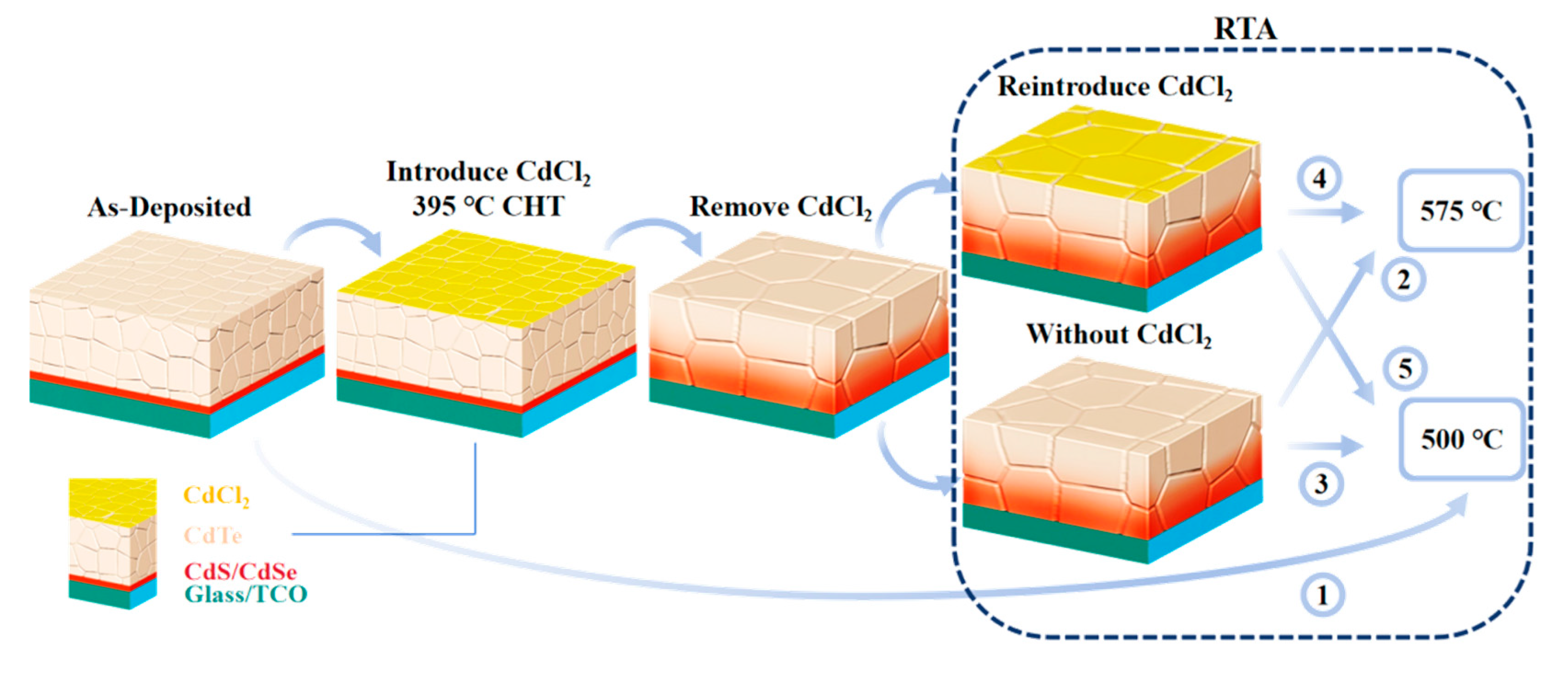
Figure 3: Schematic diagram of CHT and RTA processes.
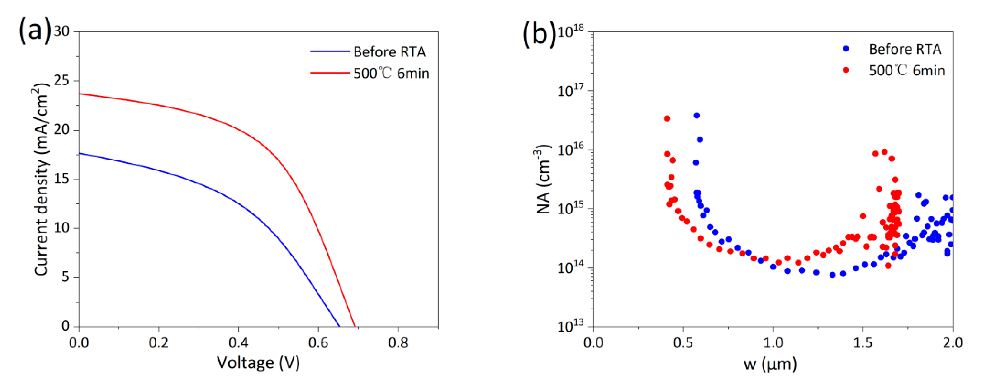
Figure 4: (a) Light J-V curves of devices without CHT before and after RTA. (b) C-V measurements of devices without CHT before and after RTA.
Table 3: Performance parameters from light J-V curves of devices without CHT before and after RTA.
| Eff (%) | Jsc (mA/cm2) | Voc (mV) | FF (%) | Rs (Ω·cm2) | Rsh (Ω·cm2) | |
|---|---|---|---|---|---|---|
| Before RTA | 5.03 | 17.67 | 653 | 43.57 | 16.09 | 122.99 |
| 500°C 6 min | 8.54 | 23.73 | 691 | 52.05 | 9.14 | 187.28 |
Baseline cells were activated by RTA at 575°C for 10 min, as shown in Process ② in Fig. 3. This condition has been validated for single-crystal device activation [17]. Fig. 5a,b shows the J-V and EQE curves before and after activation, respectively, with performance parameters listed in Table 4. Device efficiency decreased significantly after RTA and the EQE response also degraded. No obvious changes were observed visually from the glass side before and after RTA, but oxidation traces were present on the back surface of the absorber layer, analyzed in detail later. Clearly, polycrystalline CdSeTe devices have much lower tolerance to high temperatures compared to single-crystal CdTe devices, which can be rapidly cooled from temperatures close to 1000°C [16,23]. Activation rate is positively correlated with annealing temperature, making As activation more challenging in polycrystalline CdSeTe than in single-crystal CdTe. Simply applying single-crystal activation conditions to polycrystalline devices is not advisable.
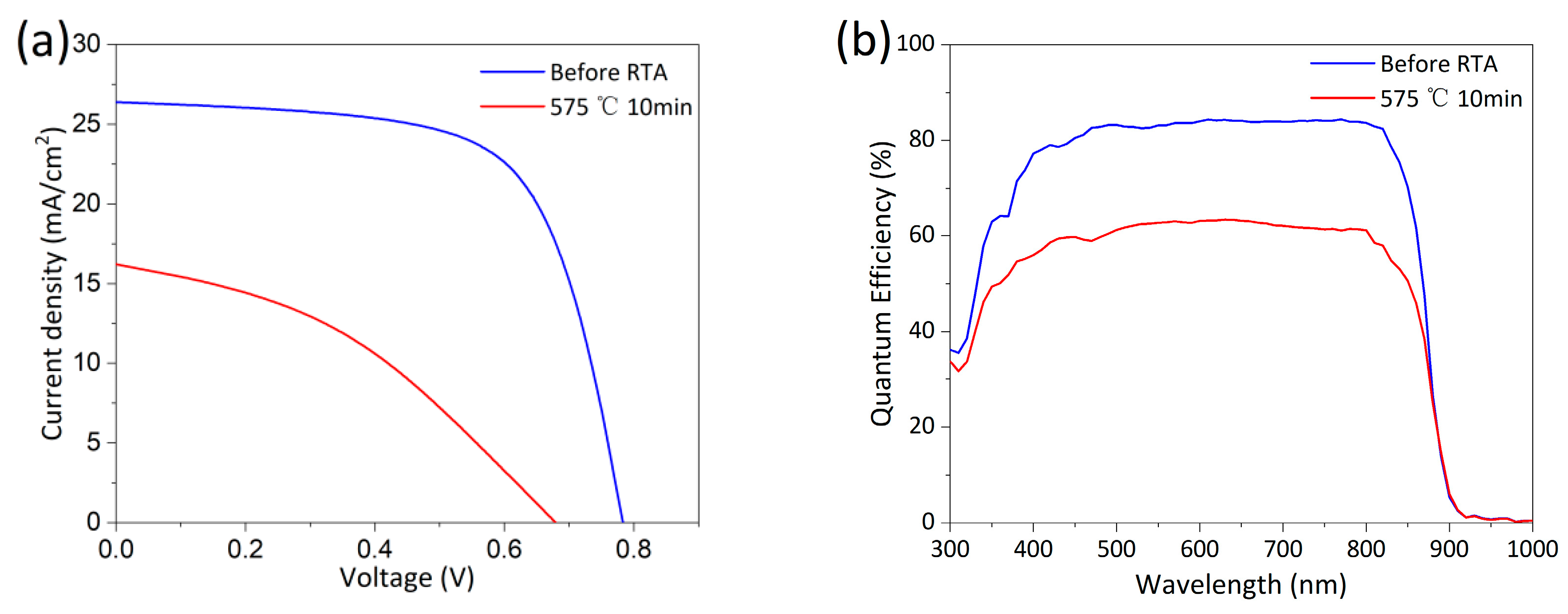
Figure 5: (a) Light J-V curves of baseline cells before and after RTA at 575°C for 10 min. (b) EQE curves of baseline cells before and after RTA at 575°C for 10 min.
Table 4: Performance parameters from light J-V curves of baseline cells before and after RTA at 575°C for 10 min.
| Eff (%) | Jsc (mA/cm2) | Voc (mV) | FF (%) | Rs (Ω·cm2) | Rsh (Ω·cm2) | |
|---|---|---|---|---|---|---|
| Before RTA | 13.57 | 26.40 | 783 | 65.65 | 4.66 | 606.93 |
| 575°C 10 min | 4.25 | 16.21 | 679 | 38.55 | 24.26 | 127.69 |
Baseline cells were activated by RTA at 500°C, as shown in Process ③ in Fig. 3. Fig. 6a shows the light J-V curves of devices with different annealing times, and their performance parameters are listed in Table 5. Compared with the baseline cell, the efficiency of activated cells changed little within 3 min, likely because the absorber layer reaches a limited temperature when the annealing time is short. Efficiency slightly decreased for the 5 min device and significantly decreased for the 10 min device, though it remained higher than the sample annealed at 575°C from Fig. 5a. Fig. 6b shows the EQE curves of devices with different annealing times. The EQE curves show little difference up to 5 min but decreased significantly at 10 min, especially in the short-wavelength range. Fig. 6d shows the C-V measurements of samples annealed for up to 5 min. A significant increase in carrier concentration, from 8.4 × 1013 cm−3 to 2.5 × 1014 cm−3, is observed after just 5 min of RTA. This result demonstrates that RTA rapidly activates doping in samples that have undergone CHT, a finding consistent with literature reports [17]. It also confirms the limited influence of Cl on the doping activation process. The C-V curves of the sample after 3 min of RTA is basically consistent with that of the base cell, which once again demonstrates that if the RTA time is too short, the actual temperature reached by the sample is insufficient to activate doping. It also verifies that the C-V curves of samples from the same base cell exhibit good consistency. This experiment, together with the experiment without CHT in Fig. 4b, demonstrates that RTA can increase carrier concentration for cells both with and without prior CHT. However, although carrier concentration increased after RTA, device efficiency decreased. This suggests that other phenomena occur concurrently with RTA and negatively impact the device, and this effect should be related to Cl diffusion, as discussed in detail in the following. Note that after annealing at 500°C for 10 min, no significant difference was observed at the front interface, while oxidation traces were present on the back surface, which darkened in color. Oxides are predominantly CdTeO3, commonly found under annealing conditions above 450°C [24]. CdTeOx phases were also observed in our previous air-annealed samples [25]. However, the RTA-treated samples showed more pronounced oxidation traces. This enhanced oxidation occurred because the RTA was performed in unsealed air (without degassing) to facilitate rapid sample extraction from the tube furnace for cooling, thereby exposing the samples to more oxygen. All samples in Fig. 6a were etched with Br-MeOH solution before Au deposition to remove the back surface oxide. To further exclude the influence of the back surface oxide on device performance, we placed the 500°C RTA before CHT without performing etching to remove the back surface oxide layer. Fig. 6c shows the light J-V curve of this sample. Its efficiency is comparable to or even higher than the baseline cell efficiency. Some studies have shown that the surface oxides formed after prolonged low-temperature annealing may actually enhance device performance, which is inconsistent with the phenomenon we observed [26]. This indicates that the presence of the back surface oxide is not the main factor causing device efficiency degradation. Interface damage at high temperatures or Cl diffusion from the front interface and grain boundaries into the grain interiors during RTA are considered the primary suspects for the performance loss.
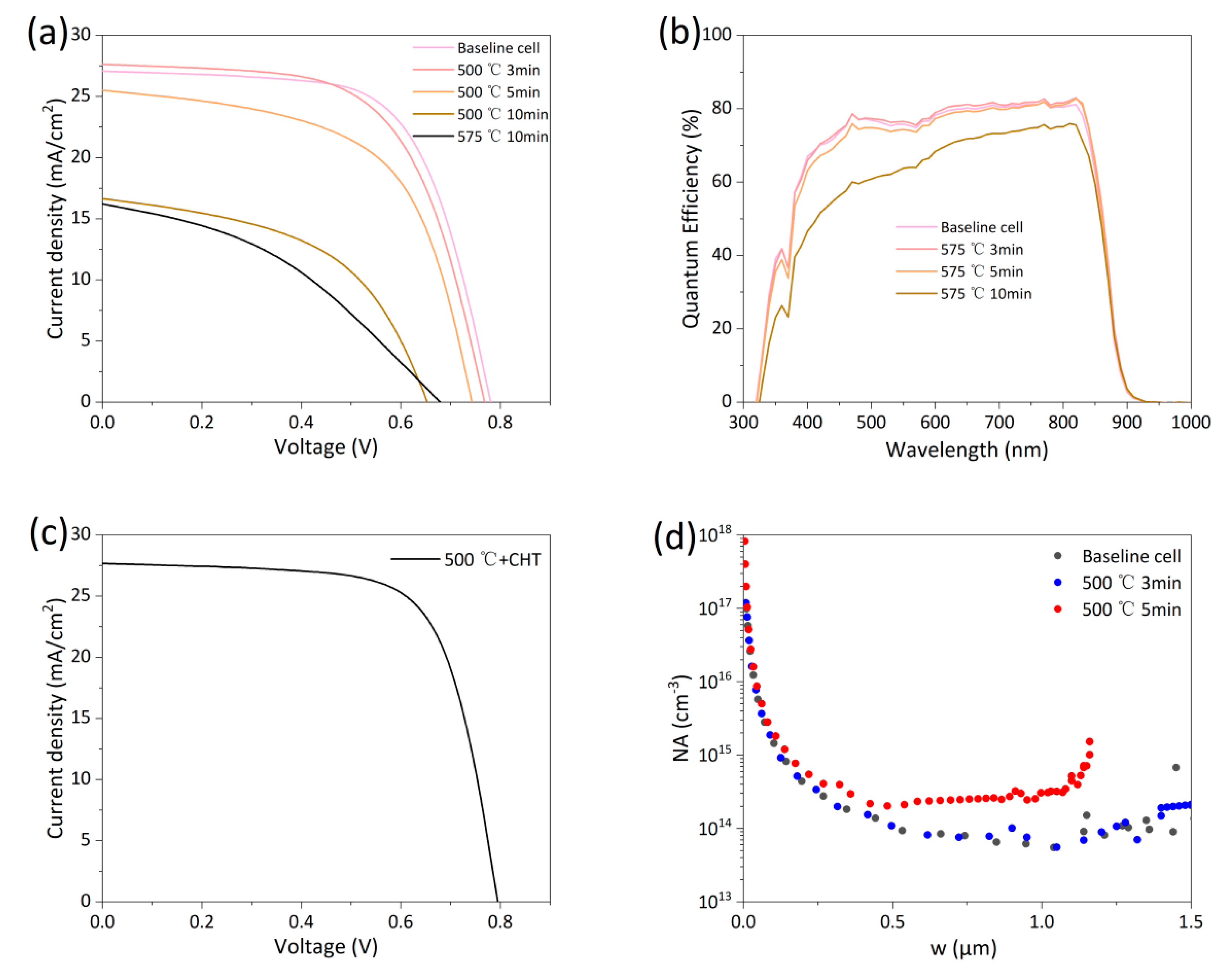
Figure 6: (a) Light J-V curves of baseline cells after RTA at 500°C for different times. (b) EQE curves of baseline cells after RTA at 500°C for different times. (c) Light J-V curve of devices subjected to 500°C, 10 min RTA first, followed by CHT. (d) C-V measurements of baseline cells after RTA at 500°C for up to 5 min.
Table 5: Performance parameters from light J-V curves of baseline cells after RTA at 500°C for different times.
| Eff (%) | Jsc (mA/cm2) | Voc (mV) | FF (%) | Rs (Ω·cm2) | Rsh (Ω·cm2) | |
|---|---|---|---|---|---|---|
| Baseline cell | 13.73 | 27.07 | 781 | 64.96 | 5.28 | 787.02 |
| 500°C 3 min | 13.10 | 27.63 | 768 | 61.68 | 5.59 | 666.98 |
| 500°C 5 min | 11.08 | 25.51 | 743 | 58.45 | 5.38 | 243.08 |
| 500°C 10 min | 5.49 | 16.65 | 654 | 50.40 | 10.44 | 186.86 |
Fig. 7a–d shows cross-sectional SEM images of the FTO/absorber interface for the baseline cell and samples before and after RTA at 500°C from Fig. 6a. No obvious differences were observed between absorber and FTO, consistent with visual inspection. This observation differs from the phenomenon of interface separation caused by excessive grain growth reported in the literature [27]. It is easily explained: typically, grain recrystallization and growth occur during CHT, where CdCl2 acts as a flux and is continuously replenished. During RTA, even at elevated temperature, the residual CdCl2 in the absorber layer is insufficient to support significant grain growth. Previous work reported that upon secondary annealing in a CdCl2-free atmosphere, Cl is removed from the grain boundaries and interiors, thereby becoming undetectable via EDS. This depletion, which in turn facilitates the reappearance of stacking faults, ultimately leads to a significant degradation in device performance [28]. However, comparing the cross-sectional EDS line scans of the various samples from Fig. 6a shown in Fig. 7e, we found that the Cl concentration did not change significantly after RTA for different times. Fig. 7f shows cross-sectional EDS mapping. The maps for different devices show no obvious differences, and Cl EDS signals persist even after annealing in a CdCl2-free atmosphere. This suggests the possibility that Cl diffuses from grain boundaries and the front interface into the grain interiors. Since the volume occupied by grain interiors is much larger than that of grain boundaries and interfaces, even complete diffusion would only marginally increase the Cl concentration within the grains, consistent with the EDS measurement results. CdCl2 can passivate grain boundaries and interface defects and eliminate stacking faults. Studies show that Cl can occupy up to 25% of Te sites when saturated at grain boundaries [29], and a two-dimensional CdCl2 layer exists at the front interface [30]. High-efficiency devices should maintain Cl saturation at grain boundaries and interface. During RTA, Cl diffuses into the grain interiors without replenishment from the ambient CdCl2 atmosphere, potentially leading to insufficient Cl content at grain boundaries or the front interface, causing device performance degradation.
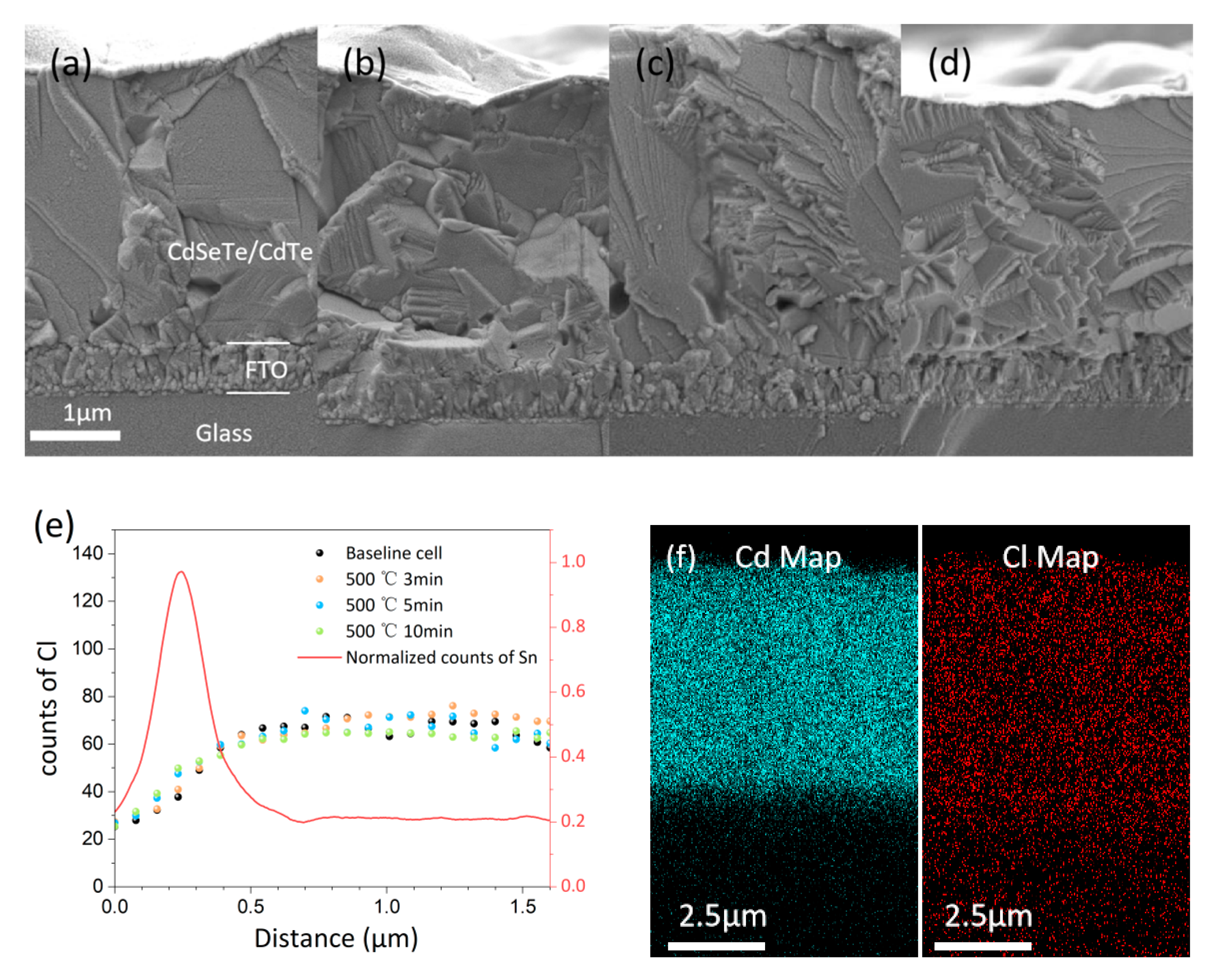
Figure 7: (a–d) Cross-sectional SEM images of the baseline, 3 min, 5 min, and 10 min samples from Fig. 6a, respectively. (e) Smoothed cross-sectional EDS line scans, calibrated by aligning the Sn peak positions. The red line shows the normalized Sn EDS line scan. (f) Cross-sectional EDS maps for Cd and Cl, showing little variation between samples.
Literature reports that devices subjected to secondary annealing in a CdCl2-free atmosphere can recover their original efficiency after undergoing CHT again [28]. However, to maintain dopant activation, CdCl2 vapor must be appropriately retained at high temperatures. Baseline cells were sprayed with a small amount of CdCl2 aqueous solution followed by RTA at 575°C, as shown in Process ④ in Fig. 3. The CdCl2 solution concentration used was 20 g/L, with spray durations of 20 s or 40 s. Fig. 8a shows the light J-V curves of devices subjected to Process ④, with performance parameters listed in Table 6. All devices after RTA showed significant performance degradation compared to the baseline cell, consistent with the performance change observed in Fig. 5a without CdCl2 atmosphere. However, the device efficiency was higher when a 20 s CdCl2 spray was applied compared with no CdCl2 atmosphere. Note that the baseline cells underwent optimized CHT. Extending CHT time leads to over-treatment and performance degradation, indicating the baseline cells were already fully chlorine-treated. The improvement in device performance with CdCl2 during RTA suggests that the Cl content in the cell has not reached the optimal concentration, supporting the hypothesis of Cl diffusion from the front interface or grain boundaries. Fig. 8b shows the EQE of the devices from Fig. 8a. When RTA was performed at 575°C, the device EQE decreased, especially in the short-wavelength range. The effect often occurs in insufficiently annealed devices, indicating severe front interface recombination. EQE shows some improvement under an appropriate amount of CdCl2 vapor during RTA. The performance of the device sprayed with CdCl2 for 20 s did not recover to baseline cell efficiency as reported in literature, possibly due to insufficient CdCl2. However, when the CdCl2 spray time was extended to 40 s, efficiency decreased again, with signs of over-treatment appearing at the front interface. Even with a 40 s spray time during RTA, the amount of CdCl2 accumulated on the back surface is only about 18% of that under the standard 395°C CHT condition, yet it significantly impacted device performance in a short time. The excessively high diffusion rate of Cl at high temperatures is a major reason for the renewed performance degradation. The difficulty in controlling CdCl2 diffusion rate at high temperatures led us to adopt a two-step annealing process rather than a single high-temperature CHT step, allowing us to study the impact of RTA on cell performance after the Cl content in the baseline cell reached its optimal concentration. Baseline cells were sprayed with CdCl2 solution for 40 s and then subjected to milder RTA at 500°C, as shown in Process ⑤ in Fig. 3. Based on Fig. 6a, polycrystalline CdTe devices tolerate RTA well for up to 5 min, so the time was set within 5 min. Their light J-V curves are shown in Fig. 8c and performance parameters are listed in Table 7. Compared to RTA without CdCl2, device efficiency increased after 500°C annealing. Fig. 8d shows the EQE of samples from Fig. 8c, which remained essentially unchanged before and after RTA. A low-concentration CdCl2 atmosphere during RTA can stabilize the device’s current. The increase in Voc should be attributed to As activation; only when other device performance parameters do not degrade can the increased carrier concentration from As activation lead to an improved Voc. The performance of the 3 min sample is lower than the 5 min sample because the shorter annealing time results in a lower achievable temperature, leading to less pronounced As activation. The reason for the lower device efficiency in Fig. 8c is the lower efficiency of the baseline cell. Typically, we would select groups with higher baseline cell efficiency for analysis. However, the RTA process in a CdCl2 atmosphere is difficult to control, and only a few groups avoided over-treatment. Even so, the performance change trend of the samples in Fig. 8c after RTA is significantly different from that of samples under other RTA conditions, so the comparison between them is still valuable for analysis.
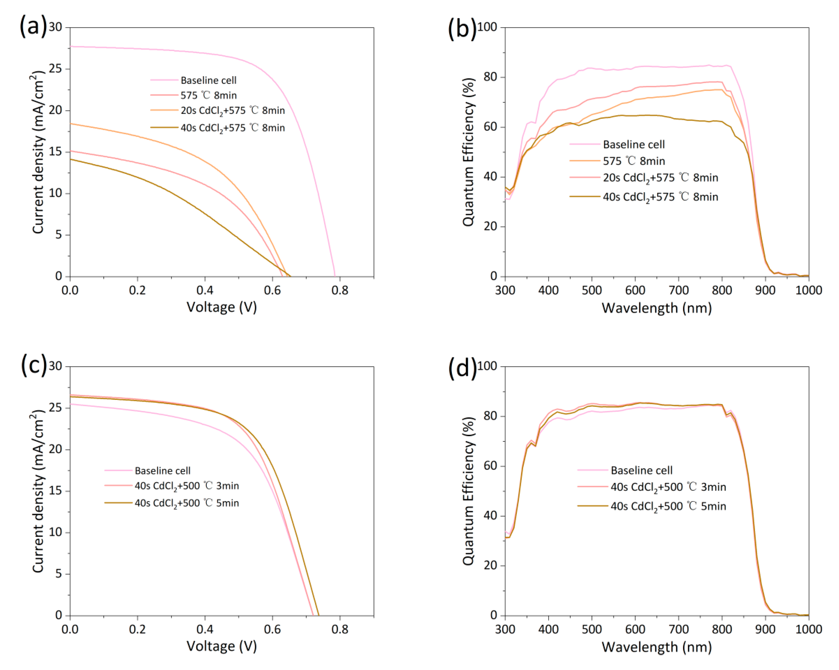
Figure 8: (a) Light J-V curves of baseline cells exposed to 0 s/20 s/40 s CdCl2 spray before and after RTA at 575°C for 8 min. (b) EQE curves of baseline cells exposed to 0 s/20 s/40 s CdCl2 spray before and after RTA at 575°C for 8 min. (c) Light J-V curves of baseline cells exposed to 0 s/40 s CdCl2 spray before and after RTA at 500°C for different times. (d) EQE curves of baseline cells exposed to 0 s/40 s CdCl2 spray before and after RTA at 500°C for different times.
Table 6: Performance parameters from light J-V curves of baseline cells exposed to 0 s/20 s/40 s CdCl2 spray before and after RTA at 575°C for 8 min.
| Eff (%) | Jsc (mA/cm2) | Voc (mV) | FF (%) | Rs (Ω·cm2) | Rsh (Ω·cm2) | |
|---|---|---|---|---|---|---|
| Baseline cell | 14.26 | 27.74 | 787 | 65.32 | 5.01 | 796.96 |
| 575°C 8 min | 4.47 | 15.16 | 632 | 46.69 | 12.70 | 151.03 |
| 20 s CdCl2 + 575°C 8 min | 5.63 | 18.45 | 645 | 58.45 | 11.59 | 143.71 |
| 40 s CdCl2 + 575°C 8 min | 3.12 | 14.16 | 648 | 34.02 | 32.38 | 105.06 |
Table 7: Performance parameters from light J-V curves of baseline cells exposed to 0 s/40 s CdCl2 spray before and after RTA at 500°C for different times.
| Eff (%) | Jsc (mA/cm2) | Voc (mV) | FF (%) | Rs (Ω·cm2) | Rsh (Ω·cm2) | |
|---|---|---|---|---|---|---|
| Baseline cell | 10.51 | 25.05 | 721 | 57.15 | 7.52 | 260.03 |
| 40 s CdCl2 + 500°C 3 min | 11.48 | 26.61 | 721 | 59.83 | 7.32 | 412.93 |
| 40 s CdCl2 + 500°C 5 min | 11.78 | 26.39 | 738 | 60.53 | 6.83 | 454.27 |
This study utilized CSS evaporation of a CdTe:As source to achieve in-situ As doping, which led to a significant efficiency enhancement compared to undoped devices. To prevent over-treatment typically induced by high-temperature CHT, RTA was applied to chlorine-treated baseline cells to activate the As dopants. The results indicate that RTA effectively activates As in devices regardless of prior CHT, and that this activation can be completed within a short time. The oxide layer formed on the back surface during RTA was found to have no significant impact on device performance.
Interface characterization revealed that at high temperatures, the residual CdCl2 within the absorber layer is insufficient to promote grain growth to an extent that would separate the FTO and absorber layer. However, Cl diffusion from grain boundaries and the front interface was observed to considerably degrade device efficiency. It was also demonstrated that introducing a trace amount of CdCl2 vapor during RTA plays a stabilizing role in maintaining device performance.
Acknowledgement:
Funding Statement: The authors received no specific funding for this study.
Author Contributions: The authors confirm contribution to the paper as follows: Conceptualization, Yuzhe Gu; methodology, Jingquan Zhang; validation, Yuzhe Gu; formal analysis, Guanggen Zeng, Xia Hao, Lili Wu, Jingquan Zhang; investigation, Yuzhe Gu; resources, Wenwu Wang, Lili Wu, Jingquan Zhang; data curation, Yuzhe Gu; writing—original draft preparation, Yuzhe Gu; writing—Yuzhe Gu, Jingquan Zhang; supervision, Jingquan Zhang; project administration, Yuzhe Gu; funding acquisition, Wenwu Wang, Guanggen Zeng, Xia Hao, Lili Wu, Jingquan Zhang. All authors reviewed and approved the final version of the manuscript.
Availability of Data and Materials: Not applicable.
Ethics Approval: Not applicable. This study did not involve human or animal subjects.
Conflicts of Interest: The authors declare that they have no known competing financial interests or personal relationships that could have appeared to influence the work reported in this paper.
Abbreviations
The following abbreviations are used in this manuscript:
| RTA | Rapid thermal annealing |
| As | Arsenic |
| CHT | Chlorine heat treatment |
| CSS | Close-space sublimation |
| J-V | Current density–voltage |
| EQE | External quantum efficiency |
References
1. Photovoltaic Research . Interactive best research-cell efficiency chart [Internet]. Golden, CO, USA: NREL; 2024 [cited 2026 Jan 1]. Available from: https://www.nrel.gov/pv/interactive-cell-efficiency.html. [Google Scholar]
2. Lustig ZF , Shimpi T , Munshi A , Shah A , Hill B , Sampath WS . CuCl treatment variations in high efficiency polycrystalline CdSexTe1−x/CdTe thin film solar cells. IEEE J Photovolt. 2022; 12( 6): 1428– 34. doi:10.1109/JPHOTOV.2022.3199116. [Google Scholar] [CrossRef]
3. Li DB , Song Z , Bista SS , Alfadhili FK , Awni RA , Shrestha N , et al. CuSCN as the back contact for efficient ZMO/CdTe solar cells. Materials. 2020; 13( 8): 1991. doi:10.3390/ma13081991. [Google Scholar] [CrossRef]
4. Lin XL , Zhao WX , Wu QC , Zhang YF , Mahabaduge H , Liu XX . Development of ZnTe film with high copper doping efficiency for solar cells. Chinese Phys B. 2022; 31( 10): 108802. doi:10.1088/1674-1056/ac6b27. [Google Scholar] [CrossRef]
5. Dzhafarov TD , Yesilkaya SS , Yilmaz Canli N , Caliskan M . Diffusion and influence of Cu on properties of CdTe thin films and CdTe/CdS cells. Sol Energy Mater Sol Cells. 2005; 85( 3): 371– 83. doi:10.1016/j.solmat.2004.05.007. [Google Scholar] [CrossRef]
6. Moore A , Fang T , Sites J . Cu profiles in CdTe solar cells. In: Proceedings of the 2015 IEEE 42nd Photovoltaic Specialist Conference (PVSC); 2015 Jun 14–19; New Orleans, LA, USA. doi:10.1109/PVSC.2015.7356091. [Google Scholar] [CrossRef]
7. Zheng X , Li B , Wang Z , Zhang DT , Feng LH , Zhang JQ , et al. Cu deep level center in CdTe solar cell. Acta Physica Sinica. 2010; 59( 4): 2783– 8. doi:10.7498/aps.59.2783. [Google Scholar] [CrossRef]
8. Evani V , Khan M , Collins S , Palekis V , Morel D , Ferekides C . Phosphorus doping of polycrystalline CdTe. In: Proceedings of the 2016 IEEE 43rd Photovoltaic Specialists Conference (PVSC); 2016 Jun 5–10; Portland, OR, USA. doi:10.1109/PVSC.2016.7749628. [Google Scholar] [CrossRef]
9. Manoukian GA , Fai C , Du B , Shafarman WN , Hages CJ , Baxter JB . Carrier dynamics and photoluminescence in antimony-doped CdTe and CdSeTe. In: Proceedings of the 2024 IEEE 52nd Photovoltaic Specialist Conference (PVSC); 2024 Jun 9–14; Seattle, WA, USA. doi:10.1109/PVSC57443.2024.10749542. [Google Scholar] [CrossRef]
10. Xiang X , Gehrke A , Tong Y , Dunham ST . Multiscale modeling and optimization of group V doping and compensation in CdSexTe1−x. ACS Appl Energy Mater. 2025; 8( 2): 1248– 65. doi:10.1021/acsaem.4c02744. [Google Scholar] [CrossRef]
11. Kujovic L , Liu X , Togay M , Abbas A , Law AM , Jones LO , et al. Development of ZnO buffer layers for As-doped CdSeTe/CdTe solar cells with efficiency exceeding 20%. Adv Mater Technol. 2025; 10( 13): 2401364. doi:10.1002/admt.202401364. [Google Scholar] [CrossRef]
12. Mallick R , Li X , Reich C , Shan X , Zhang W , Nagle T , et al. Arsenic-doped CdSeTe solar cells achieve world record 22.3% efficiency. IEEE J Photovoltaics. 2023; 13( 4): 510– 5. doi:10.1109/jphotov.2023.3282581. [Google Scholar] [CrossRef]
13. Wu J , Gan Y , Liu J , Su Y , Zhou Y , Wan M , et al. Synergistic light–heat–bias activation for 21%-efficient CdSeTe thin-film solar cells. ACS Energy Lett. 2026; 11( 1): 573– 80. doi:10.1021/acsenergylett.5c03194. [Google Scholar] [CrossRef]
14. Neupane S , Li DB , Abudulimu A , Jamarkattel MK , Jiang CS , Xian Y , et al. Ex situ bismuth doping for efficient CdSeTe thin-film solar cells with open-circuit voltages exceeding 900 mV. Joule. 2025; 9( 1): 101766. doi:10.1016/j.joule.2024.09.013. [Google Scholar] [CrossRef]
15. Hussain Z , Phillips AB , Friedl JD , Hussain ZN , Kaluarachchi PN , ElSayed H , et al. In situ arsenic doping of evaporated CdTe films using an integrating effusion cell—reaching 3% activation ratio. In: Proceedings of the 2024 IEEE 52nd Photovoltaic Specialist Conference (PVSC); 2024 Jun 9–14; Seattle, WA, USA. doi:10.1109/PVSC57443.2024.10749014. [Google Scholar] [CrossRef]
16. Nagaoka A , Kuciauskas D , Scarpulla MA . Doping properties of cadmium-rich arsenic-doped CdTe single crystals: Evidence of metastable AX behavior. Appl Phys Lett. 2017; 111( 23): 232103. doi:10.1063/1.4999011. [Google Scholar] [CrossRef]
17. Mathew AT , Lott H , Colegrove E , Young MR , Kuciauskas D , Wolden CA , et al. Arsenic activation and compensation in single crystal CdTe bilayers. J Appl Phys. 2025; 137( 11): 115702. doi:10.1063/5.0246994. [Google Scholar] [CrossRef]
18. Wang B , Yu P , Li Y , Xu Q , Zhang Y , Jie W . Structural, defect, and photoelectric characterization of CdTe-based single crystals grown by a vertical Bridgman method. Mater Charact. 2025; 223: 114899. doi:10.1016/j.matchar.2025.114899. [Google Scholar] [CrossRef]
19. Jamarkattel MK , Phillips AB , Quader A , Subedi KK , Alfadhili FK , Bista SS , et al. Incorporation of arsenic in CdSe/CdTe solar cells during close spaced sublimation of CdTe:As. In: Proceedings of the 2020 47th IEEE Photovoltaic Specialists Conference (PVSC); 2020 Jun 15–Aug 21; Calgary, AB, Canada. p. 2605– 8. doi:10.1109/pvsc45281.2020.9300772. [Google Scholar] [CrossRef]
20. Danielson A , Munshi A , Kindvall A , Swain SK , Barth K , Lynn K , et al. Doping CdTe absorber cells using group V elements. In: Proceedings of the 2018 IEEE 7th World Conference on Photovoltaic Energy Conversion (WCPEC) (A Joint Conference of 45th IEEE PVSC, 28th PVSEC & 34th EU PVSEC); 2018 Jun 10–15; Waikoloa Village, HI, USA. doi:10.1109/pvsc.2018.8547792. [Google Scholar] [CrossRef]
21. Perkins CL , McGott DL , Reese MO , Metzger WK . SnO2-catalyzed oxidation in high-efficiency CdTe solar cells. ACS Appl Mater Interfaces. 2019; 11( 13): 13003– 10. doi:10.1021/acsami.9b00835. [Google Scholar] [CrossRef]
22. Rahman MH , Rojsatien S , Krasikov D , Chan MK , Bertoni M , Mannodi-Kanakkithodi A . First principles investigation of dopants and defect complexes in CdSexTe1−x. Sol Energy Mater Sol Cells. 2025; 293: 113857. doi:10.1016/j.solmat.2025.113857. [Google Scholar] [CrossRef]
23. Nagaoka A , Kimura K , Ang AK , Takabayashi Y , Yoshino K , Sun Q , et al. Direct observation of group-V dopant substitutional defects in CdTe single crystals. J Am Chem Soc. 2023; 145( 16): 9191– 7. doi:10.1021/jacs.3c01248. [Google Scholar] [CrossRef]
24. Bai Z , Wang D . Oxidation of CdTe thin film in air coated with and without a CdCl2 layer. Phys Status Solidi A. 2012; 209( 10): 1982– 7. doi:10.1002/pssa.201228107. [Google Scholar] [CrossRef]
25. Liu GM , Hu G , Tang P , Wu LL , Hao X , Zeng GG , et al. Study of the effect of CdCl2 introduction on the high temperature activation treatment of CdTe:As polycrystalline thin films. Chalcogenide Lett. 2024; 21( 10): 797– 808. doi:10.15251/cl.2024.2110.797. [Google Scholar] [CrossRef]
26. Rugen-Hankey SL , Clayton AJ , Barrioz V , Kartopu G , Irvine SJC , McGettrick JD , et al. Improvement to thin film CdTe solar cells with controlled back surface oxidation. Sol Energy Mater Sol Cells. 2015; 136: 213– 7. doi:10.1016/j.solmat.2014.10.044. [Google Scholar] [CrossRef]
27. Amarasinghe M , Colegrove E , Moseley J , Moutinho H , Albin D , Duenow J , et al. Obtaining large columnar CdTe grains and long lifetime on nanocrystalline CdSe, MgZnO, or CdS layers. Adv Energy Mater. 2018; 8( 11): 1702666. doi:10.1002/aenm.201702666. [Google Scholar] [CrossRef]
28. Abbas A , Swanson D , Munshi A , Barth KL , Sampath WS , West GD , et al. The effect of a post-activation annealing treatment on thin film CdTe device performance. In: Proceedings of the 2015 IEEE 42nd Photovoltaic Specialist Conference (PVSC); 2015 Jun 14–19; New Orleans, LA, USA. p. 1– 6. doi:10.1109/pvsc.2015.7356441. [Google Scholar] [CrossRef]
29. Mao D , Wickersham CE , Gloeckler M . Measurement of chlorine concentrations at CdTe grain boundaries. IEEE J Photovoltaics. 2014; 4( 6): 1655– 8. doi:10.1109/jphotov.2014.2357258. [Google Scholar] [CrossRef]
30. McGott DL , Muzzillo CP , Perkins CL , Berry JJ , Zhu K , Duenow JN , et al. 3D/2D passivation as a secret to success for polycrystalline thin-film solar cells. Joule. 2021; 5( 5): 1057– 73. doi:10.1016/j.joule.2021.03.015. [Google Scholar] [CrossRef]
Cite This Article
 Copyright © 2026 The Author(s). Published by Tech Science Press.
This work is licensed under a Creative Commons Attribution 4.0 International License , which permits unrestricted use, distribution, and reproduction in any medium, provided the original work is properly cited.
 Downloads
 Citation Tools