
 Submit a Paper
 Propose a Special lssue
 Open Access
ARTICLE

Spin-Coated Kesterite Based CZTS (Cu2ZnSnS4) Thin Films: Structural, Optical, and Compositional Analysis for Photovoltaic Applications
1 Physics Discipline, Science, Engineering and Technology School, Khulna University, Khulna, Bangladesh
2 Institute of Energy Research and Development (IERD), Bangladesh Council of Scientific and Industrial Research (BCSIR), Dhaka, Bangladesh
3 Department of Physics, Faculty of Arts and Science (FSA), Bangladesh Army University of Science and Technology, Khulna, Bangladesh
* Corresponding Authors: Muhammad Shahriar Bashar. Email: ; Md. Salahuddin Mina. Email:
Chalcogenide Letters 2026, 23(3), 1 https://doi.org/10.32604/cl.2026.079270
Received 18 January 2026; Accepted 03 March 2026; Issue published 03 April 2026
 View Full Text
 Download PDF
Abstract
In this work, spin-coated Cu2ZnSnS4 (CZTS) thin films with systematically varied thicknesses were investigated to understand their influence on structural, compositional, and optical properties relevant to high-performance photovoltaic applications. CZTS absorber layers were fabricated using a sol-gel spin-coating technique, which offers simplicity, low cost, and excellent thickness control, followed by annealing at 450°C under a nitrogen atmosphere to promote crystallization and phase formation. X-ray diffraction (XRD) analysis revealed that films with a thickness of approximately 608 nm exhibited the highest crystallinity and a preferred orientation along the (112) plane, indicating enhanced structural order and improved grain connectivity. Raman spectroscopy further confirmed the formation of single-phase kesterite CZTS, with no detectable secondary phases, ensuring material purity. Scanning electron microscopy (SEM) images demonstrated compact, uniform grains, while energy-dispersive X-ray spectroscopy (EDX) analysis indicated a slightly Cu-rich and Zn-poor composition, consistent with typical solution-processed CZTS films. Optical characterization using UV-Vis spectroscopy revealed strong absorption in the visible region, with absorption coefficients exceeding 104 cm−1, highlighting the material’s suitability for efficient light harvesting. The direct optical bandgap was estimated to range from 1.48 to 1.53 eV, achieving an optimal value of 1.50 ± 0.02 eV for the ten-layer film. Urbach energy values (0.57–0.78 eV) suggested the presence of defect-related localized states associated with grain boundaries and compositional variations. Overall, this work demonstrates that careful thickness optimization significantly enhances the microstructural, compositional, and optical properties of CZTS thin films, providing valuable insights for the design, fabrication, and optimization of efficient kesterite-based photovoltaic absorber layers for practical solar cell applications.Keywords
Kesterite Cu2ZnSnS4 (CZTS) thin films have emerged as promising candidates for earth-abundant, non-toxic solar cells due to their tunable direct bandgap (~1.5 eV), high absorption coefficient (α ≥ 104 cm−1), and low-cost fabrication potential [1,2,3]. Unlike other absorber materials, such as CIGS and CdTe, CZTS is composed of earth-abundant, non-toxic elements, making it economically viable and environmentally friendly [4]. However, despite these benefits, the power conversion efficiency of CZTS-based solar cells remains considerably below their theoretical limit, mainly due to inherent flaws, cation disorder, band tailing, and the creation of secondary phases. These difficulties create deep-level trap states, increase non-radiative recombination, and impair charge transport, therefore constraining device performance [5,6].
CZTS thin films typically crystallize in the kesterite structure, where sulfur anions tetrahedrally coordinate the metal cations (Cu, Zn, Sn) [7,8,9]. The high sulfur content can promote secondary phase formation, posing challenges for achieving single-phase films [10]. Controlling film composition and thickness is therefore critical for optimizing structural, optical, and electronic properties. Although several studies have explored CZTS stoichiometry, annealing conditions, and precursor types, systematic investigations of thickness-dependent structural and optical properties for spin-coated CZTS films are limited [11,12]. Film thickness influences crystallinity, grain size, defect density, bandgap, and Urbach energy, which collectively determine photovoltaic performance. In particular, an optimal thickness is necessary to balance light absorption and carrier collection, since excessively thin films suffer from inadequate absorption while overly thick films cause recombination losses and structural defects. Therefore, precise thickness control is a vital aspect in achieving high-quality CZTS absorber layers.
In this work, spin-coated CZTS thin films with 5–20 layers (~400–1000 nm) were fabricated and systematically analyzed. Microstructural parameters (crystallite size, dislocation density, micro-strain) were extracted from XRD, SEM was used to examine grain morphology, and optical properties including bandgap and Urbach energy were studied. Comparison with recent high-impact literature demonstrates the potential of these films for high-efficiency CZTS solar cells, providing a foundation for future device fabrication and interface optimization [13,14].
To synthesize CZTS thin-film absorber, 40 mL of 2-methoxy ethanol (CH3O·CH2·CH2OH) was used to dissolve copper-chloride dihydrate (CuCl2·2H2O), zinc-chloride (ZnCl2), stannous chloride (SnCl2·2H2O), and thiourea (SC(NH2)2). The concentrations of these compounds were 0.24 M, 0.12 M, 0.08 M, and 0.96 M, correspondingly. The mixture was stirred on a magnetic hotplate at 55°C for 10 min. Subsequently, 7 drops of ethanolamine (C2H7NO) were added as a stabilizer, and stirring continued for an additional 50 min at 55°C to yield a homogeneous, transparent yellow sol-gel solution.
Absorber layers were deposited on SLG substrate using a spin coater (SPS SPIN 150) at a final rotation speed of 3000 rpm for a total of 27.5 s, divided into two sequential steps: 15.5 s and 12.0 s. The rotation speed ramped up at a rate of 500 rpm/s. After placing the substrate on the chuck and centering it, 5 drops of solution were dispensed at the center. The substrate was then dried at 140°C for 10 min and allowed to cool for 5 min to form a single layer (Fig. 1). This procedure was repeated 5, 10, 15, and 20 times to obtain film thicknesses of 459 nm, 608 nm, 822 nm, and 1005 nm, respectively. Finally, the films were annealed at 450°C for 40 min under N2 atmosphere.
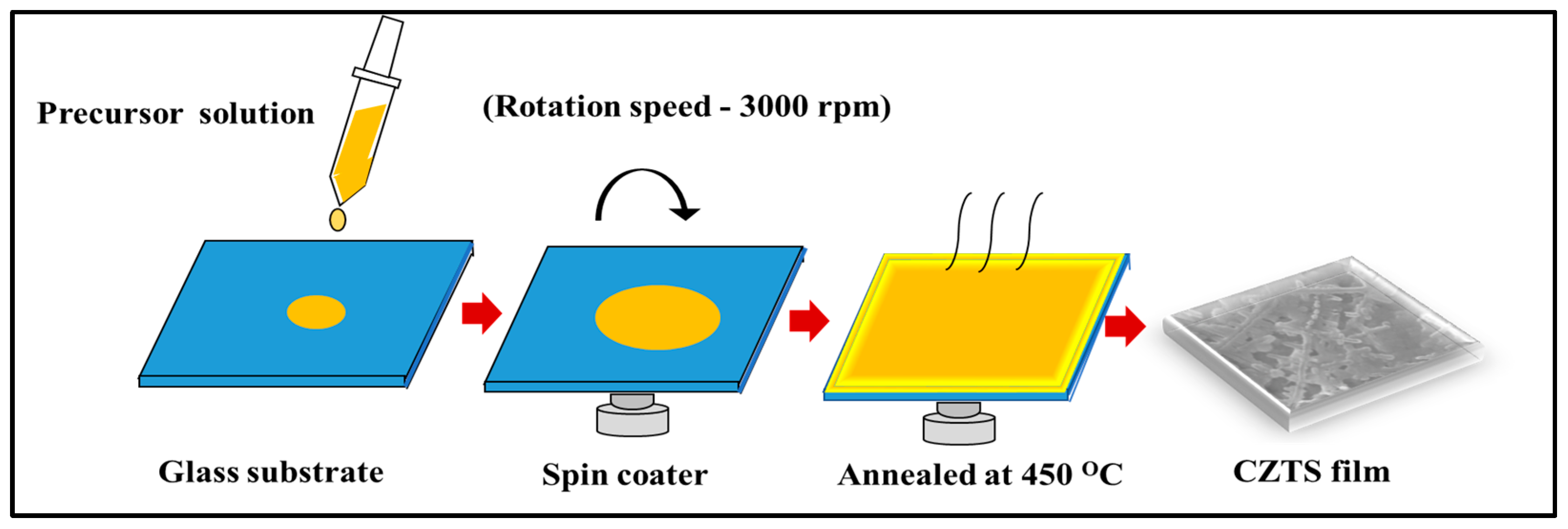
Figure 1: Schematic of Spin-coating process for thin film absorber layers.
The film thickness was estimated using a stylus profilometer, a technique widely employed for its high precision in quantifying the thickness of thin films, coatings, and surface layers, which is displayed in Table 1.
Table 1: Thickness of different layers.
| Layer | Thickness (nm) |
|---|---|
| 5 | 459 |
| 10 | 608 |
| 15 | 822 |
| 20 | 1005 |
3.1.1 X-Ray Diffraction (XRD) Analysis
The crystalline structure of the sol-gel-processed CZTS absorbers was examined using an X-ray diffractometer (GBC, EMMA) operated at 35 kV and 28 mA, with Cu-Kα radiation (λ = 1.5406 Å). The diffraction patterns were recorded over a 2θ range of 20°–80°. The XRD patterns (Fig. 2) confirm that all films are polycrystalline tetragonal kesterite CZTS, with dominant peaks at 2θ~28.54°, 47.45°, and 56.26° corresponding to the (112), (220), and (312) planes. These peak positions are in good agreement with the standard ICDD data (JCPDS No. 26-0575), indicating the formation of phase-pure kesterite CZTS.
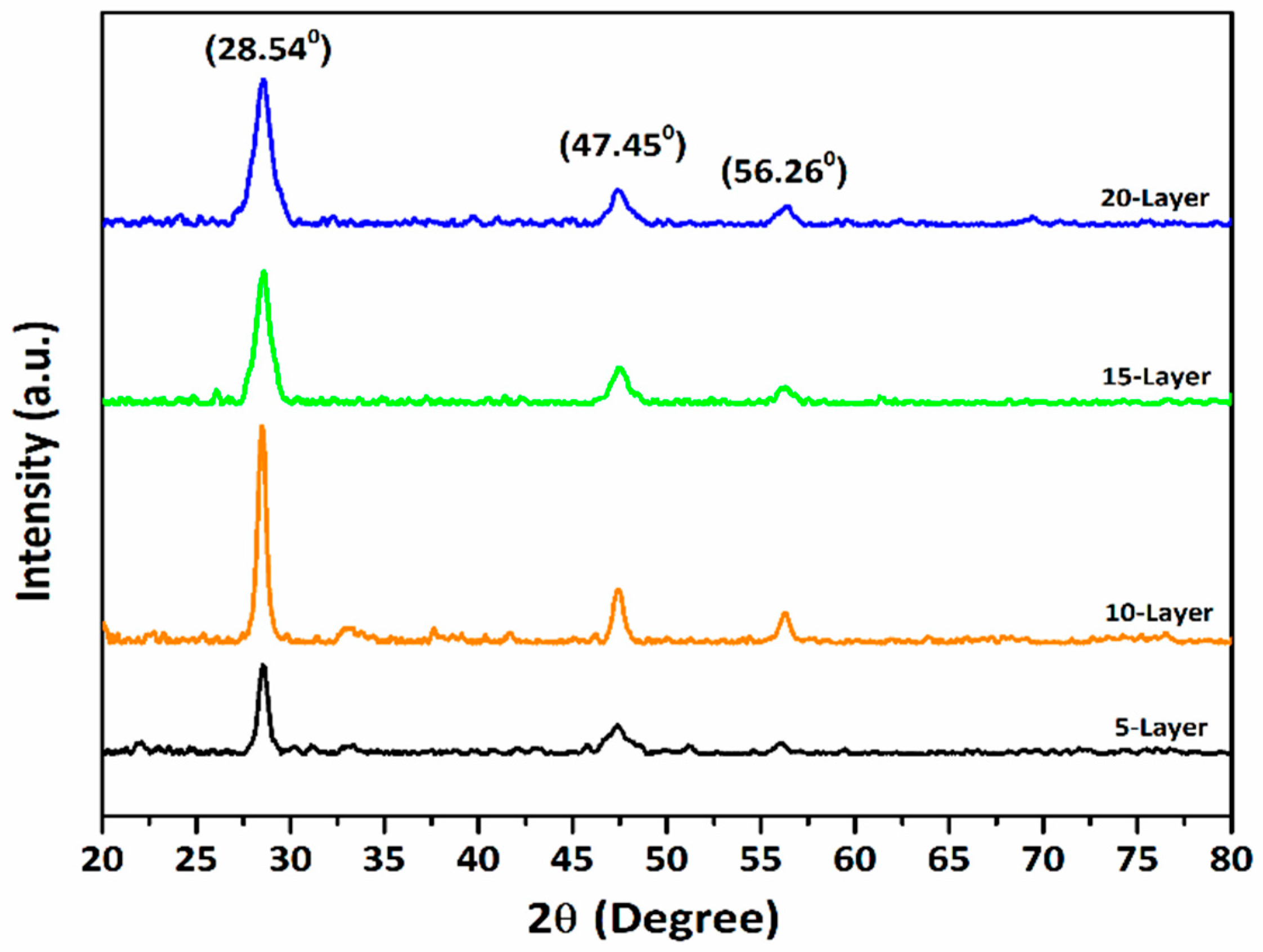
Figure 2: XRD patterns for CZTS absorber layers.
The narrow full width at half maximum (FWHM) values and the sharper diffraction peaks indicate enhanced crystallinity and improved microstructural quality of the films. Lower FWHM values and reduced dislocation density suggest fewer lattice defects, which are critical for absorber layer performance in photovoltaic applications [15]. Grain size plays a vital role in determining the performance of CZTS solar cells, as larger grains reduce grain boundary recombination and facilitate efficient charge transport [12]. Among the studied samples, the 10-layer film with a thickness of approximately 608 nm exhibits the sharpest diffraction peak and the lowest FWHM, indicating superior crystalline quality and larger crystallite size.
To evaluate the size of the crystallite (D), the Debye-Scherrer formula was applied [16].
The X-ray wavelength, denoted by
The 10-layer CZTS absorber exhibits the narrowest FWHM (0.53°) and the largest crystallite size (15.47 nm), reflecting improved crystallinity (Table 2). The dislocation density (
In nanostructured materials, internal lattice strain is often induced by crystal dislocations, which disrupt the ideal arrangement of atoms within the lattice. Based on the isotropic strain model of Williamson-Hall (W-HISM), lattice strain and crystallite size are considered to be independent parameters [18]. However, the anisotropic Williamson-Hall model based on uniform deformation energy density (W-HUDEDM) suggests that as crystallite size decreases, the increase in volume defects at grain boundaries, due to enhanced strain energy concentration. The dislocation density of the present CZTS thin films varies from 4.17849 × 10¹⁵ to 1.48 × 10¹⁶ lines/m2, depending on film thickness. These values are comparable to those reported for solution-processed CZTS thin films. For instance, dislocation densities on the order of 1015–1016 lines/m2 have been reported for sol-gel and spin-coated CZTS absorber layers [19,20]. The comparable defect density indicates that the films prepared in this study possess microstructural quality consistent with well-crystallized CZTS absorbers, which is beneficial for efficient charge transport and reduced recombination losses. As shown in Table 2, the 10-layer CZTS thin film exhibits the lowest dislocation density (
The variation of crystallite size, dislocation density, and lattice strain clearly indicates that the 10-layer CZTS film possesses the most optimized microstructural properties. The reduced defect density and minimal strain at this thickness can be attributed to improved nucleation and grain growth processes, resulting in enhanced crystallinity and superior structural quality [21,22]. As shown in Fig. 3, lower FWHM values correspond to larger crystallite size and lower dislocation density, confirming improved crystal quality.
Table 2: The CZTS thin films’ microstructural characteristics in the (112) plane.
| Layers | 2 | d-Spacing ( | FWHM, | Crystallite Size, D (nm) | Dislocation Density, | Strain, ε (×10−3) |
|---|---|---|---|---|---|---|
| 5 | 28.54 | 1.612 | 0.61 | 13.44 | 5.53607E+15 | 10.47 |
| 10 | 28.54 | 1.612 | 0.53 | 15.47 | 4.17849E+15 | 9.10 |
| 15 | 28.54 | 1.612 | 0.84 | 9.76 | 1.04979E+16 | 14.40 |
| 20 | 28.54 | 1.612 | 1.00 | 8.20 | 1.48721E+16 | 17.16 |
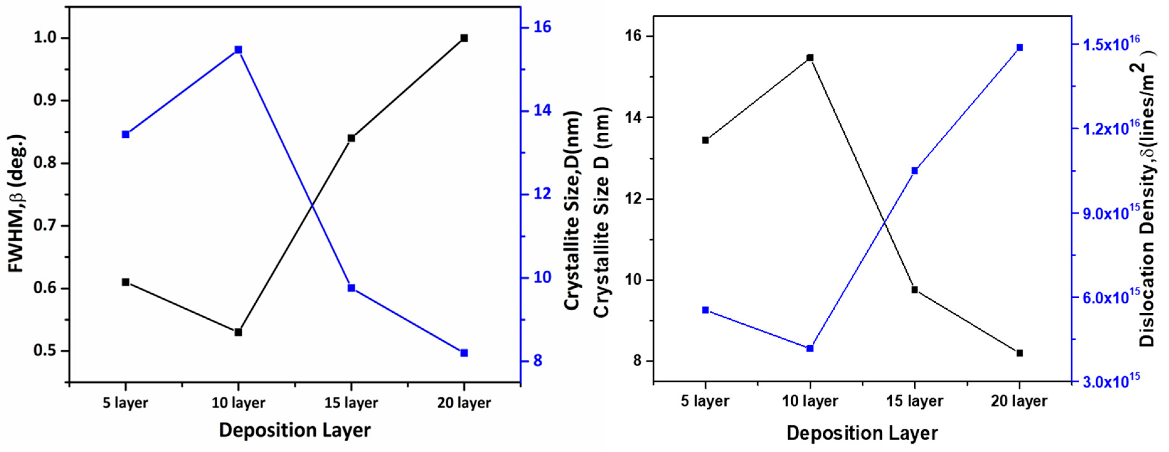
Figure 3: Variation of FWHM (β), crystallite size and dislocation density with film thickness.
It should be noted that the crystallite size calculated from XRD represents coherently diffracting domain size, which is generally smaller than the surface grain size observed in SEM micrographs. The SEM micrographs indicate that the films consist of agglomerated grains formed by the joining of multiple nanocrystallites, which explains the apparent difference between the XRD-derived crystallite size (8–15 nm) and the larger surface features.
3.1.2 Raman Spectroscopic Analysis
Raman spectroscopy was employed to further verify phase purity and to identify possible secondary phases. Raman spectra were recorded in the wavenumber range of 140–495 cm−1, as shown in Fig. 4. All samples exhibit a prominent Raman peak at approximately 328 cm−1, characteristic of kesterite CZTS, in agreement with reported literature [9,23]. No additional peaks corresponding to secondary phases such as orthorhombic Cu2SnS3, cubic ZnS, SnS2, or Cu2−xS were detected. Notably, the absence of Raman signatures associated with Cu2−xS conductive secondary phases indicates that although the films exhibit slight Cu-rich composition, the formation of detrimental shunting phases was effectively suppressed. This observation confirms that CZTS nanoparticles in a single phase were successfully produced for every solvent [23,24].
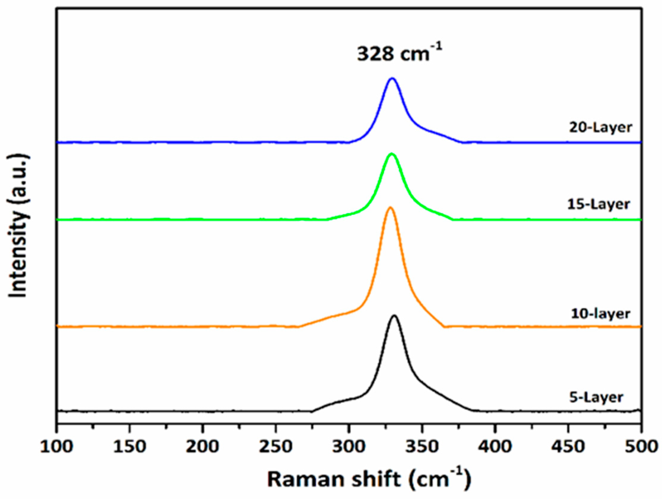
Figure 4: Raman spectra of CZTS thin film absorber layers.
Among all samples, the 10-layer film displays the highest Raman peak intensity and sharpness, confirming superior crystallinity and phase purity. Thus, the combined XRD and Raman analyses confirm the formation of well-crystallized, phase-pure polycrystalline CZTS absorber layers.
3.2 Morphological and Compositional Characterization
The surface morphology of CZTS thin films was examined using scanning electron microscopy (SEM, EVO 18, Zeiss), as shown in Fig. 5a–d. The micrographs reveal a tight and linked granular structure, resembling entangled nanoscale networks. The 5-layer film exhibits noticeable gaps and microcracks, while increasing the deposition layers leads to a significant reduction of these structural imperfections. The 10-layer film displays dense, uniform grains with minimal voids, indicating improved film compactness and surface uniformity.
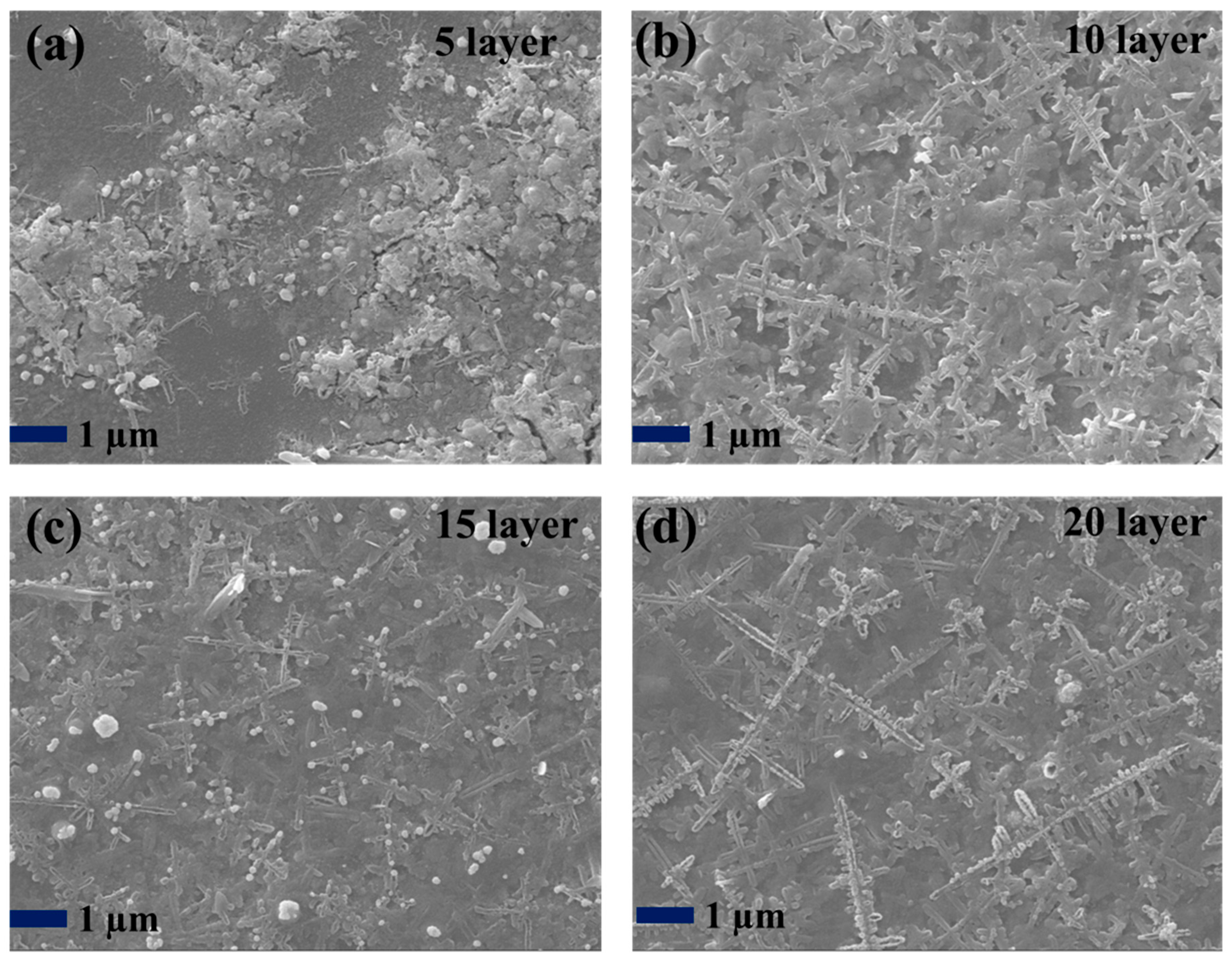
Figure 5: SEM images of CZTS absorber layers: (a) 5 layer, (b) 10 layer, (c) 15 layer, and (d) 20 layer.
This morphological evolution can be explained by the nucleation growth mechanism described by Shinde et al. [25]. Initially, metal ions form nucleation sites on the substrate, followed by sulfur incorporation and CZTS production. Subsequent grain expansion and coalescence lead to bigger crystalline domains, resulting in denser and more compact films with increasing thickness. The morphological enhancement observed in the 10-layer film is consistent with the XRD data, which also reveal better crystallinity and optimized microstructural quality.
The elemental composition of the films was examined using energy-dispersive X-ray spectroscopy (EDX). The related spectra (Fig. 6) and quantitative data presented in Table 3 demonstrate that all samples exhibit slight Cu-rich and Zn-poor compositions compared to the ideal stoichiometric ratio. Such compositional deviation is commonly observed in solution-processed CZTS films and is attributed to the higher mobility of Cu ions and the higher volatility of Zn and S species during annealing [26,27,28].
Table 3: Chemical composition data for CZTS absorber layers.
| Layers | Cu % | Zn % | Sn % | S % | Cu/Zn | Zn/Sn |
|---|---|---|---|---|---|---|
| 5 | 36.43 | 13.05 | 5.77 | 44.76 | 2.79 | 2.26 |
| 10 | 30.78 | 14.53 | 8.04 | 46.65 | 2.12 | 1.81 |
| 15 | 33.98 | 12.00 | 7.40 | 46.62 | 2.83 | 1.62 |
| 20 | 32.96 | 12.46 | 8.17 | 46.41 | 2.65 | 1.53 |
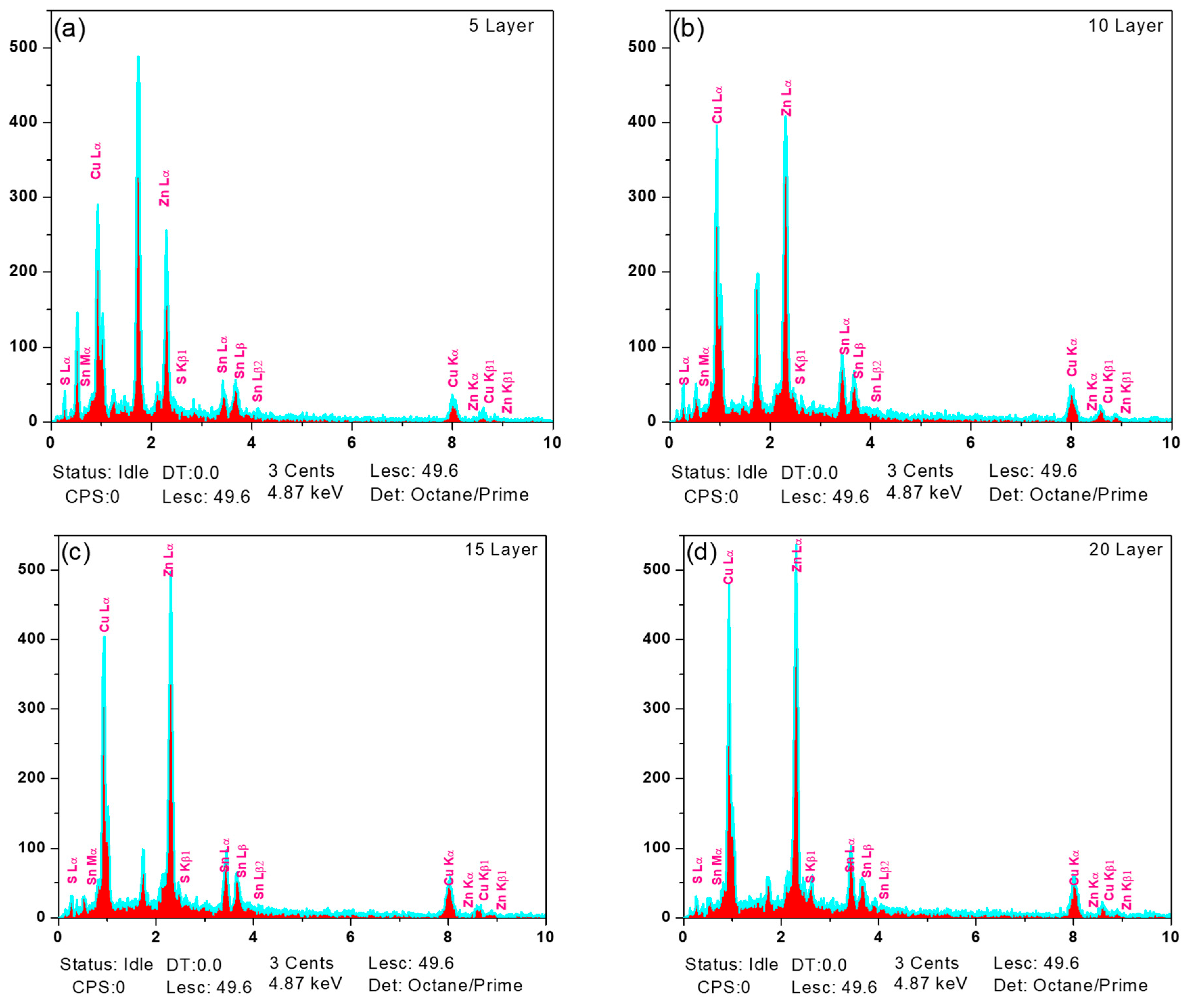
Figure 6: EDX spectra of CZTS absorber layers for different film thicknesses: (a) 5 layer, (b) 10 layer, (c) 15 layer, and (d) 20 layer.
Although Cu-rich compositions can improve single-phase development, excessive Cu content may lead to the development of highly conductive Cu2−xS phases, which reduce solar cell efficiency by introducing shunting routes. However, Raman analysis shows the absence of such detrimental secondary phases, showing that the Cu-rich state stays within an acceptable range. Among all samples, the 10-layer film exhibits the most balanced stoichiometry, approaching the ideal Cu:Zn:Sn:S ratio of 2:1:1:4, consistent with its superior structural and morphological properties [29].
The optical properties of CZTS thin films were examined through the utilization of a UV-visible spectrophotometer operating in the 400–1000 nm wavelength range. Fig. 7 shows the variation of absorption coefficient (α) with photon energy. All samples exhibit strong absorption in the visible region, with absorption coefficients exceeding 104 cm−1, confirming their suitability as absorber layers for photovoltaic applications [24,30].
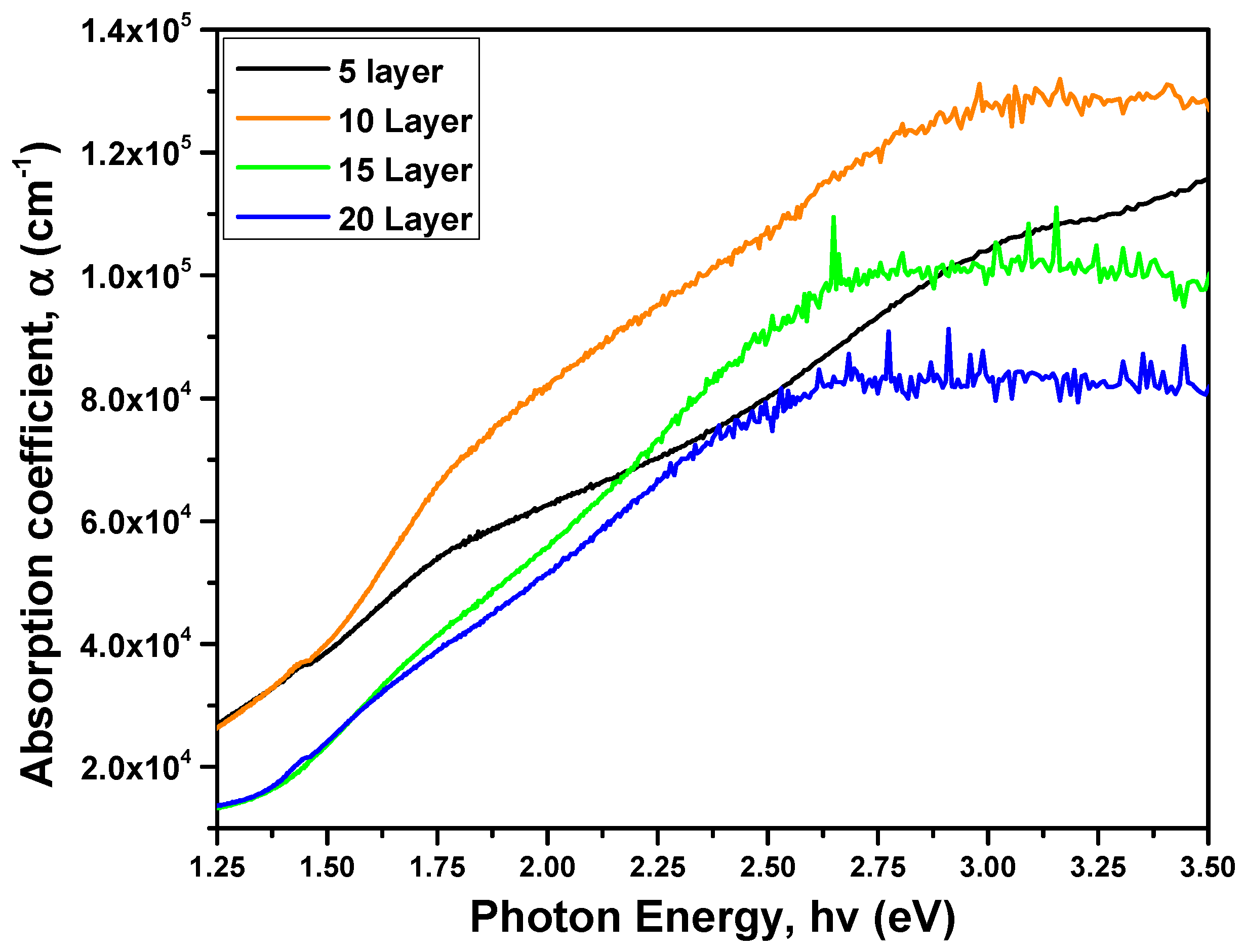
Figure 7: Absorption coefficient
The absorbance can be used to compute the absorption coefficient using Lambert-Beer’s law [31],
The optical bandgap (
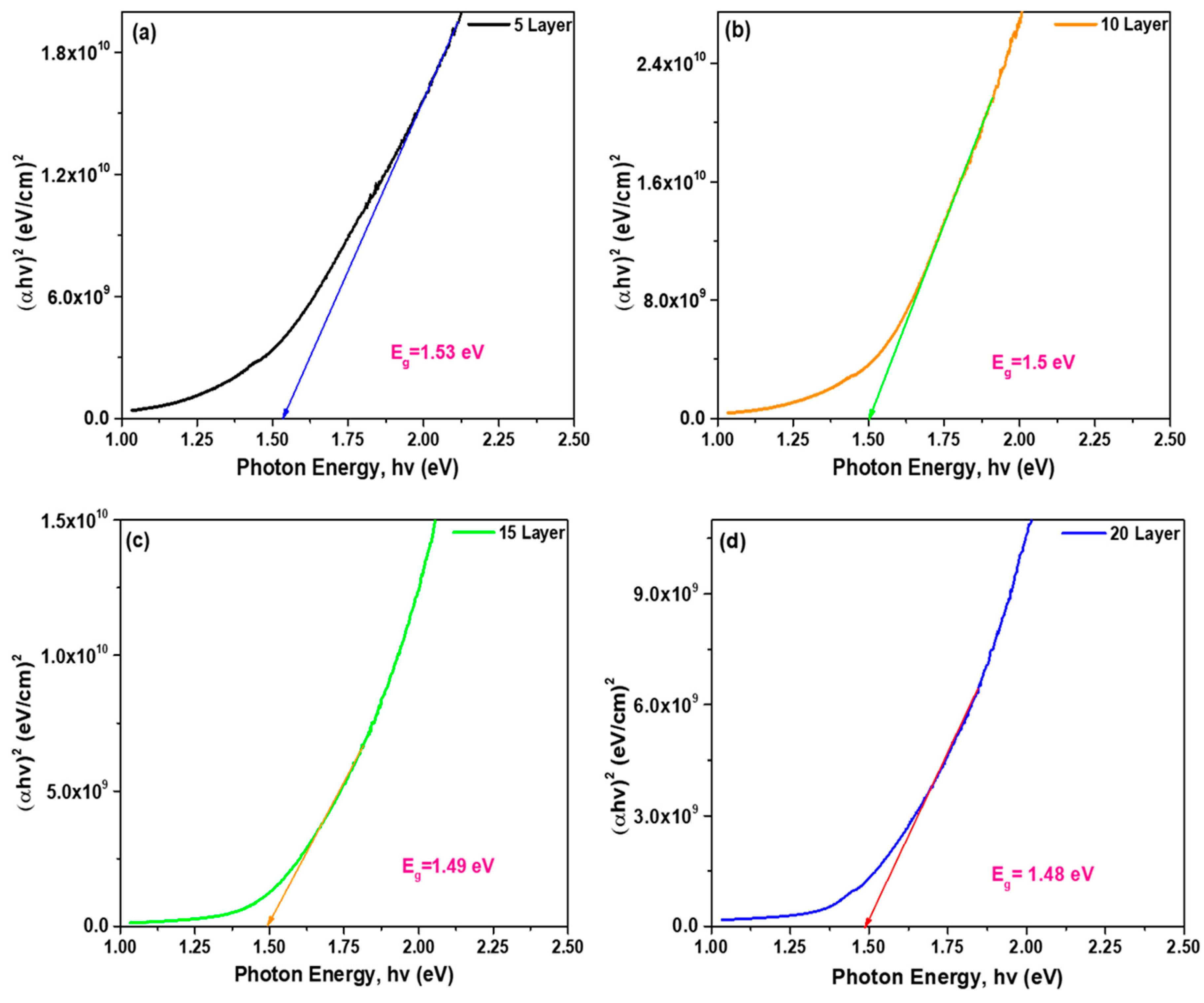
Figure 8: Bandgap calculation of CZTS absorber layers: (a) 5 layer, (b) 10 layer, (c) 15 layer, and (d) 20 layer.
The linear extrapolation of these plots yields direct bandgap energies ranging from 1.48 to 1.53 eV (Table 4), which are close to the ideal bandgap (~1.5 eV) for single-junction solar cell applications [32]. The estimated uncertainty in the extracted bandgap values is ±0.02 eV, primarily arising from the linear fitting procedure. The obtained band gap values are consistent with previously reported CZTS thin films, which typically exhibit band gaps in the range of 1.45–1.55 eV depending on deposition technique and composition.
Table 4: Band gap, dielectric constant, and refractive index (n) values calculated for CZTS absorber layers.
| Layers | Band Gap, | Refractive Index, n | High-Frequency Dielectric Constant, | Dielectric Constant, | Urbach Energy, |
|---|---|---|---|---|---|
| 5 | 1.53 | 2.898 | 8.398 | 13.808 | 0.63 |
| 10 | 1.50 | 2.913 | 8.486 | 13.90 | 0.57 |
| 15 | 1.49 | 2.918 | 8.515 | 13.931 | 0.67 |
| 20 | 1.48 | 2.923 | 8.544 | 13.962 | 0.78 |
A slight reduction in bandgap with increasing film thickness is observed, which can be attributed to improved crystallinity and reduced quantum confinement effects in thicker films [26,33].
The Urbach energy (EU), which reflects the degree of structural disorder and defect density, was determined using [34]:
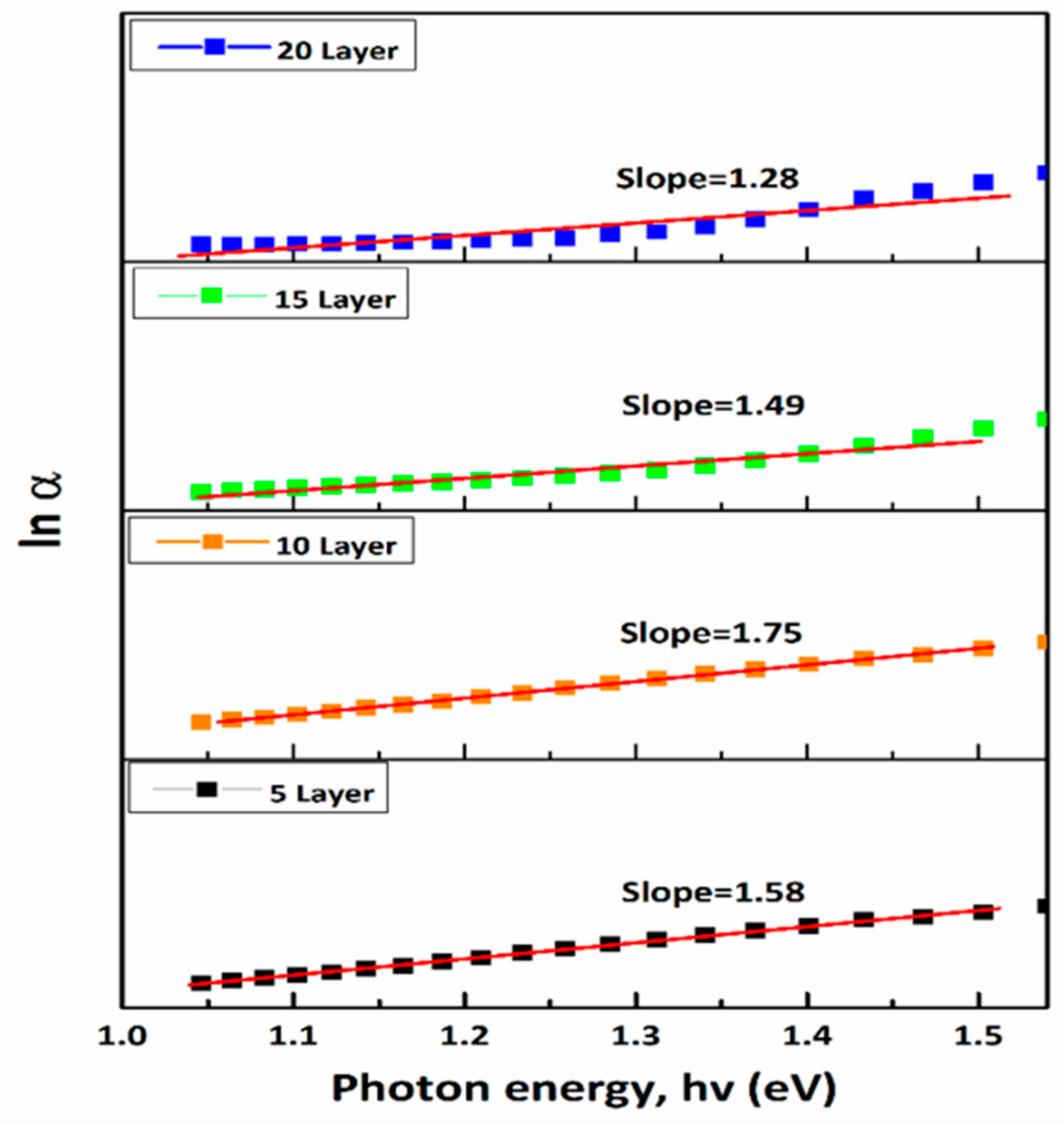
Figure 9: Dependence of ln (
The lowest Urbach energy value (0.57 eV) recorded for the 10-layer film suggests lower defect density, increased crystallinity, and enhanced optoelectronic quality. In contrast, greater Urbach energies (0.67–0.78 eV) suggest increased disorder [35], likely coming from antisite defects, grain boundary states, and compositional changes. Such defects can introduce localized states within the bandgap, enhancing non-radiative recombination and deteriorating photovoltaic performance by reducing open-circuit voltage (Voc) and fill factor (FF) [36,37,38]. Further tuning of deposition and annealing settings is expected to decrease these defect states and boost device performance. The Urbach energy values acquired in this study (0.57–0.78 eV) are analogous to those documented for solution-processed CZTS films. Higher Urbach energies (0.60–0.90 eV) have been documented as a result of structural disorder, but lower values have been attained in high-quality films produced using various methods. For example, Azmi et al. reported Urbach energies of approximately 0.29–0.35 eV, while Moreno et al. observed values below 0.40 eV for improved crystalline CZTS films. These results suggest that more modification of growth conditions could diminish defect states and enhance optoelectronic quality [39,40].
The Moss relation was applied to calculate the refractive index (n) of the CZTS thin film absorber layers analyzed in this study [26]:
Fig. 10 illustrates the inverse relationship between refractive index and bandgap. A higher refractive index (~2.5–3.0) combined with an optimal bandgap (~1.5 eV confirms the excellent optical quality of the CZTS absorber layers [36], particularly for the 10-layer film.
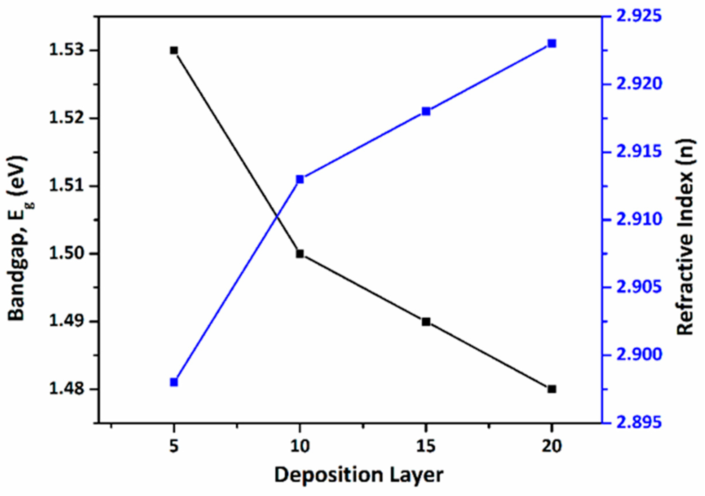
Figure 10: Relation between Refractive index (n) with Bandgap (
Spin-coated CZTS thin films with optimized thickness (~608 nm) exhibit high crystallinity, controlled microstructural properties, and an optimal direct bandgap of 1.50 ± 0.02 eV, indicating strong potential for photovoltaic applications. SEM analysis confirms that grain size increases with film thickness, correlating with XRD-derived crystallite size, while Urbach energy analysis provides insights into defects and compositional inhomogeneity. Although Cu-rich compositions promote single-phase kesterite formation, precise stoichiometry control is essential to suppress secondary Cu2−xS phases that may induce shunting pathways and reduce open-circuit voltage, as widely reported in recent studies [6,41,42].
This work develops a complete thickness-dependent framework for spin-coated CZTS thin films by integrating structural, compositional, morphological, and optical investigations. Future study should focus on full device fabrication, interface engineering, and precision stoichiometry optimization to minimize defect-assisted recombination and boost power conversion efficiency. Overall, the present findings give crucial parameters for constructing high-performance, low-cost, and earth-abundant kesterite-based photovoltaic systems.
Acknowledgement:
Funding Statement: This research was partially funded by the Research & Innovation Center (RIC), Khulna University, Bangladesh, under Grant No. KU/RIC-04/2000-310.
Author Contributions: The authors confirm contribution to the paper as follows: Conceptualization, Md. Rakib Hasan and Md. Salahuddin Mina; methodology and investigation, Md. Rakib Hasan and Mimi Mondal; formal analysis and data curation, Md. Rakib Hasan; original draft preparation, Md. Rakib Hasan; review and editing, Afrina Sharmin, Md. Salahuddin Mina, Muhammad Shahriar Bashar, Md. Ahasan Habib and Rinku Majumder; visualization and resources, Mimi Mondal; supervision, Md. Salahuddin Mina and Muhammad Shahriar Bashar; project administration and funding acquisition, Md. Salahuddin Mina. All authors reviewed and approved the final version of the manuscript.
Availability of Data and Materials: The authors confirm that the data supporting the findings of this study are available from the corresponding authors upon reasonable request.
Ethics Approval: Not applicable.
Conflicts of Interest: The authors declare no conflicts of interest.
Abbreviations
The following abbreviations are used in this manuscript:
| Cu | Copper |
| Zn | Zinc |
| Sn | Tin |
| S | Sulfur |
| XRD | X-ray diffraction |
| SEM | Scanning electron microscopy |
| EDX | Energy dispersive x-ray |
| UV | Ultraviolet |
| eV | Electron volt |
| FF | Fill factor |
| nm | Nanometer |
| Greek Letters | |
| α | Absorption coefficient |
| λ | Wavelength |
| Subscripts | |
| Eg | Bandgap |
| Voc | Open circuit voltage |
References
1. Pandharkar S , Hase Y , Shah S , Doiphode V , Waghmare A , Punde A , et al. Enhanced photoresponse of Cu2ZnSnS4 absorber thin films fabricated using multi-metallic stacked nanolayers. RSC Adv. 2023; 13( 18): 12123– 32. [Google Scholar]
2. Aka AH , Bouich A , Aka B , Soucase BM . Synthesis and characterization of kesterite Cu2ZnSn(SxSe1−x)4 thin films with low-cost for efficient solar cells. Results Opt. 2023; 13: 100507. doi:10.1016/j.rio.2023.100507. [Google Scholar] [CrossRef]
3. Wallace SK , Mitzi DB , Walsh A . The steady rise of kesterite solar cells. ACS Energy Lett. 2017; 2: 776– 9. doi:10.1021/acsenergylett.7b00131. [Google Scholar] [CrossRef]
4. Tunuguntla V , Chen WC , Shih PH , Shown I , Lin YR , Hwang JS , et al. A nontoxic solvent based sol–gel Cu2ZnSnS4 thin film for high efficiency and scalable low-cost photovoltaic cells. J Mater Chem A. 2015; 3( 29): 15324– 30. doi:10.1039/C5TA02833G. [Google Scholar] [CrossRef]
5. Kumar M , Dubey A , Adhikari N , Venkatesan S , Qiao Q . Strategic review of secondary phases, defects and defect-complexes in kesterite CZTS–Se solar cells. Energy Environ Sci. 2015; 8( 11): 3134– 59. doi:10.1039/C5EE02153G. [Google Scholar] [CrossRef]
6. He M , Yan C , Li J , Suryawanshi MP , Kim J , Green MA , et al. Kesterite solar cells: Insights into current strategies and challenges. Adv Sci. 2021; 8( 9): 2004313. doi:10.1002/advs.202004313. [Google Scholar] [CrossRef]
7. Liu D , Han D , Huang M , Zhang X , Zhang T , Dai C , et al. Theoretical study on the kesterite solar cells based on Cu2ZnSn(S, Se)4 and related photovoltaic semiconductors. Chin Phys B. 2018; 27( 1): 018806. doi:10.1088/1674-1056/27/1/018806. [Google Scholar] [CrossRef]
8. Ravindiran M , Praveenkumar C . Status review and the future prospects of CZTS based solar cell–A novel approach on the device structure and material modeling for CZTS based photovoltaic device. Renew Sustain Energy Rev. 2018; 94: 317– 29. doi:10.1016/j.rser.2018.06.008. [Google Scholar] [CrossRef]
9. Hameed AM , Bakr NA , Khodair ZT . Effect of film thickness on some physical properties of sol-gel spin-coated Cu2ZnSnS4 thin films. AIP Conf Proc. 2022; 2398: 20038. doi:10.1063/5.0094379. [Google Scholar] [CrossRef]
10. Mohammed AS . The effect of replacing iron atoms instead of zinc of the quaternary compound CZTS. J Phys Conf Ser. 2021; 2114( 1): 012033. doi:10.1088/1742-6596/2114/1/012033. [Google Scholar] [CrossRef]
11. Ge J , Chu J , Jiang J , Yan Y , Yang P . Characteristics of in-substituted CZTS thin film and bifacial solar cell. ACS Appl Mater Interfaces. 2014; 6( 23): 21118– 30. doi:10.1021/am505980n. [Google Scholar] [CrossRef]
12. Sharmin A , Bashar MS , Tabassum S , Mahmood ZH . Low cost and sol-gel processed earth abundant Cu2ZnSnS4 thin film as an absorber layer for solar cell: Annealing without sulfurization. Int J Thin Film Sci Technol. 2019; 8: 67– 76. doi:10.18576/ijtfst/080206. [Google Scholar] [CrossRef]
13. Shi J , Wang J , Meng F , Zhou J , Xu X , Yin K , et al. Multinary alloying for facilitated cation exchange and suppressed defect formation in kesterite solar cells with above 14% certified efficiency. Nat Energy. 2024; 9( 9): 1095– 104. doi:10.1038/s41560-024-01551-5. [Google Scholar] [CrossRef]
14. Fu J , Yang J , Dong W , Ren S , Zhu H , Wang Y , et al. A critical review of solution-process engineering for kesterite thin-film solar cells: Current strategies and prospects. J Mater Chem A. 2024; 12( 2): 545– 66. [Google Scholar]
15. Jan ST , Noman M . Influence of absorption, energy band alignment, electric field, recombination, layer thickness, doping concentration, temperature, reflection and defect densities on MAGeI3 perovskite solar cells with Kesterite HTLs. Phys Scr. 2022; 97( 12): 125007. doi:10.1088/1402-4896/ac9e7f. [Google Scholar] [CrossRef]
16. Abuelwafa AA , Abdelhamid SM , Dongol M , Elhady AF . Thickness-dependent linear and nonlinear optical properties of spin-coated iron (III) tetraphenylporphyrin chloride thin films. Opt Mater. 2025; 168: 117447. doi:10.1016/j.optmat.2025.117447. [Google Scholar] [CrossRef]
17. Khodair ZT , Kamil AA , Abdalaah YK . Effect of annealing on structural and optical properties of Ni(1–x)MnxO nanostructures thin films. Phys B Condens Matter. 2016; 503: 55– 63. doi:10.1016/j.physb.2016.09.016. [Google Scholar] [CrossRef]
18. Shafi PM , Bose AC . Impact of crystalline defects and size on X-ray line broadening: A phenomenological approach for tetragonal SnO2 nanocrystals. AIP Adv. 2015; 5( 5): 057137. doi:10.1063/1.4921452. [Google Scholar] [CrossRef]
19. Rafique R , Tonny KN , Sharmin A , Mahmood ZH . Study on the effect of varying film thickness on the transparent conductive nature of aluminum doped zinc oxide deposited by dip coating. Mater Focus. 2018; 7( 5): 707– 13. doi:10.1166/mat.2018.1572. [Google Scholar] [CrossRef]
20. Tonny KN , Rafique R , Sharmin A , Bashar MS , Mahmood ZH . Electrical, optical and structural properties of transparent conducting Al doped ZnO (AZO) deposited by sol-gel spin coating. AIP Adv. 2018; 8( 6): 065307. doi:10.1063/1.5023020. [Google Scholar] [CrossRef]
21. Borbély A . The modified Williamson-Hall plot and dislocation density evaluation from diffraction peaks. Scr Mater. 2022; 217: 114768. doi:10.1016/j.scriptamat.2022.114768. [Google Scholar] [CrossRef]
22. Mhadhbi M , Khitouni M , Escoda L , Suñol JJ , Dammak M . Characterization of mechanically alloyed nanocrystalline Fe(Al): Crystallite size and dislocation density. J Nanomater. 2010; 2010: 712407. doi:10.1155/2010/712407. [Google Scholar] [CrossRef]
23. Sifawa AA , Shehu A . Synthesis and characterization of spin coated CZTS Thin films for solar cell applications. Caliphate J Sci Technol. 2021; 3: 158– 61. doi:10.4314/cajost.v3i2.94 [Google Scholar] [CrossRef]
24. Shinde NM , Deokate RJ , Lokhande CD . Properties of spray deposited Cu2ZnSnS4 (CZTS) thin films. J Anal Appl Pyrolysis. 2013; 100: 12– 6. doi:10.1016/j.jaap.2012.10.018. [Google Scholar] [CrossRef]
25. Shinde NM , Deshmukh PR , Patil SV , Lokhande CD . Aqueous chemical growth of Cu2ZnSnS4 (CZTS) thin films: Air annealing and photoelectrochemical properties. Mater Res Bull. 2013; 48( 5): 1760– 6. doi:10.1016/j.materresbull.2012.12.053. [Google Scholar] [CrossRef]
26. Chen S , Gong XG , Walsh A , Wei SH . Defect physics of the kesterite thin-film solar cell absorber Cu2ZnSnS4. Appl Phys Lett. 2010; 96( 2): 021902. doi:10.1063/1.3275796. [Google Scholar] [CrossRef]
27. Chen S , Yang JH , Gong XG , Walsh A , Wei SH . Intrinsic point defects and complexes in the quaternary kesterite semiconductor Cu2ZnSnS4. Phys Rev B. 2010; 81( 24): 245204. doi:10.1103/physrevb.81.245204. [Google Scholar] [CrossRef]
28. Kheraj V , Patel KK , Patel SJ , Shah DV . Synthesis and characterisation of Copper Zinc Tin Sulphide (CZTS) compound for absorber material in solar-cells. J Cryst Growth. 2013; 362: 174– 7. doi:10.1016/j.jcrysgro.2011.10.034. [Google Scholar] [CrossRef]
29. Xu J , Yang J , Jiang S , Shang S . Effects of element ratio on robustness of CZTS films: Variations in sulfurization temperature. Ceram Int. 2020; 46( 16): 25927– 34. doi:10.1016/j.ceramint.2020.07.079. [Google Scholar] [CrossRef]
30. Henry J , Mohanraj K , Sivakumar G . Electrical and optical properties of CZTS thin films prepared by SILAR method. J Asian Ceram Soc. 2016; 4( 1): 81– 4. doi:10.1016/j.jascer.2015.12.003. [Google Scholar] [CrossRef]
31. Tara A , Bharti V , Sharma S , Gupta R . Device simulation of FASnI3 based perovskite solar cell with Zn(O0.3, S0.7) as electron transport layer using SCAPS-1D. Opt Mater. 2021; 119: 111362. doi:10.1016/j.optmat.2021.111362. [Google Scholar] [CrossRef]
32. Pawar SM , Pawar BS , Moholkar AV , Choi DS , Yun JH , Moon JH , et al. Single step electrosynthesis of Cu2ZnSnS4 (CZTS) thin films for solar cell application. Electrochim Acta. 2010; 55( 12): 4057– 61. doi:10.1016/j.electacta.2010.02.051. [Google Scholar] [CrossRef]
33. Khammar M , Ynineb F , Guitouni S , Bouznit Y , Attaf N . Crystallite size and intrinsic strain contribution in band gap energy redshift of ultrasonic-sprayed kesterite CZTS nanostructured thin films. Appl Phys A. 2020; 126( 6): 398. doi:10.1007/s00339-020-03591-6. [Google Scholar] [CrossRef]
34. Benouis CE , Benhaliliba M , Juarez AS , Aida MS , Chami F , Yakuphanoglu F . The effect of indium doping on structural, electrical conductivity, photoconductivity and density of states properties of ZnO films. J Alloys Compd. 2010; 490( 1–2): 62– 7. doi:10.1016/j.jallcom.2009.10.098. [Google Scholar] [CrossRef]
35. Ebied MS , Elhady AF , Dongol M , Abuelwafa AA . Thermal annealing induced modification in linear and nonlinear optical properties of Ag/Ge20Se50S30 bilayer film. Opt Mater. 2024; 148: 114962. doi:10.1016/j.optmat.2024.114962. [Google Scholar] [CrossRef]
36. Wang W , Winkler MT , Gunawan O , Gokmen T , Todorov TK , Zhu Y , et al. Device characteristics of CZTSSe thin-film solar cells with 12.6% efficiency. Adv Energy Mater. 2014; 4( 7): 1301465. doi:10.1002/aenm.201301465. [Google Scholar] [CrossRef]
37. Gokmen T , Gunawan O , Todorov TK , Mitzi DB . Band tailing and efficiency limitation in kesterite solar cells. Appl Phys Lett. 2013; 103( 10): 103506. doi:10.1063/1.4820250. [Google Scholar] [CrossRef]
38. Shin B , Gunawan O , Zhu Y , Bojarczuk NA , Chey SJ , Guha S . Thin film solar cell with 8.4% power conversion efficiency using an earth-abundant Cu2ZnSnS4 absorber. Prog Photovolt. 2013; 21( 1): 72– 6. doi:10.1002/pip.1174. [Google Scholar] [CrossRef]
39. Azmi N , Chelvanathan P , Yusoff Y , Ferdaous MT , Zuhdi AWM , Tiong SK , et al. Enhancing microstructural and optoelectronic properties of CZTS thin films by post deposition ionic treatment. Mater Lett. 2021; 285: 129117. doi:10.1016/j.matlet.2020.129117. [Google Scholar] [CrossRef]
40. Moreno R , Ramirez EA , Gordillo Guzmán G . Study of optical and structural properties of CZTS thin films grown by co-evaporation and spray pyrolysis. J Phys Conf Ser. 2016; 687: 012041. doi:10.1088/1742-6596/687/1/012041. [Google Scholar] [CrossRef]
41. Wei H , Li Y , Cui C , Wang X , Shao Z , Pang S , et al. Defect suppression for high-efficiency kesterite CZTSSe solar cells: Advances and prospects. Chem Eng J. 2023; 462: 142121. doi:10.1016/j.cej.2023.142121. [Google Scholar] [CrossRef]
42. Boerasu I , Vasile BS . Current status of the open-circuit voltage of kesterite CZTS absorber layers for photovoltaic applications: Part I, a review. Materials. 2022; 15( 23): 8427. doi:10.3390/ma15238427. [Google Scholar] [CrossRef]
Cite This Article
 Copyright © 2026 The Author(s). Published by Tech Science Press.
This work is licensed under a Creative Commons Attribution 4.0 International License , which permits unrestricted use, distribution, and reproduction in any medium, provided the original work is properly cited.
 Downloads
 Citation Tools