
 Login
Login Register
 Submit a Paper
 Propose a Special lssue
 Open Access

Recent Breakthroughs in Leveraging MoS2 to Transcend the Performance Bottlenecks of Perovskite Solar Cells
State Key Laboratory of Smart Power Distribution Equipment and System, School of Materials Science and Engineering, Hebei University of Technology, Tianjin, China
* Corresponding Author: Cong Chen. Email:
Chalcogenide Letters 2026, 23(7), 6 https://doi.org/10.32604/cl.2026.087725
Received 22 June 2026; Accepted 23 July 2026; Issue published 07 August 2026
 View Full Text
 Download PDF
Abstract
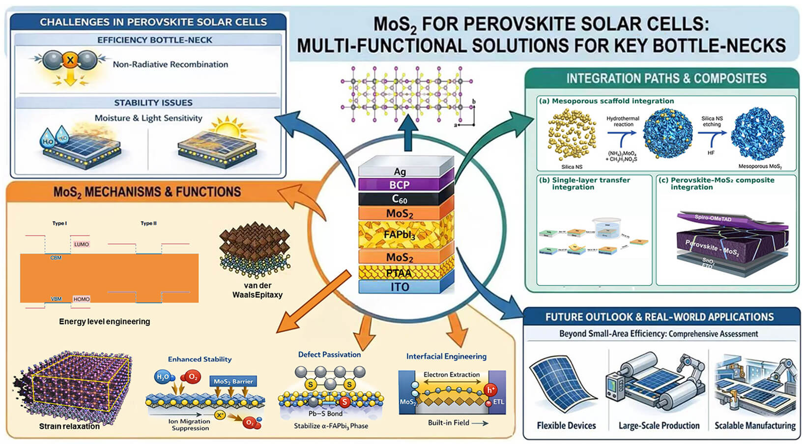
The power conversion efficiency of perovskite solar cells has increased rapidly; however, interfacial-defect-induced non-radiative recombination, ion migration, and sensitivity to moisture, oxygen, and thermal stress continue to cause open-circuit voltage losses and a limited operational lifetime. Owing to its tunable energy levels, high carrier mobility, and compact hydrophobic layered structure, two-dimensional MoS2 can serve as an electron or hole transport layer, an interfacial buffer layer, or an additive, enabling favorable energy-level alignment and optimized interfacial charge-transfer kinetics, thereby promoting carrier extraction and suppressing recombination. The sulfur sites of MoS2 can coordinate with undercoordinated Pb2+ to form Pb–S bonds, thereby passivating defects and stabilizing the α-FAPbI3 phase, while continuous MoS2 layers can suppress ion migration through physical diffusion blocking; meanwhile, van der Waals epitaxy and heterogeneous nucleation induced by MoS2 improve film crystallinity and relieve residual stress, synergistically enhancing both efficiency and durability. This review summarizes the functional mechanisms, preparation methods, and integration routes of MoS2 in PSCs, with particular attention to recent advances in wafer-scale monolayer interfaces, mesoporous electron-transport layers, functionalized nanosheet additives, quantum-dot composite absorbers, and hybrid interfaces. These approaches are compared in terms of their effects on charge transport, defect passivation, crystallization, device efficiency, stability, process compatibility, and scalability. The outlook also considers data-driven optimization, integration with other two-dimensional materials, and applications in flexible, large-area, and tandem devices.Graphic Abstract
Keywords
Over the past decade, MoS2-based perovskite optoelectronic devices have attracted considerable attention [1,2,3]. Meanwhile, the certified power conversion efficiency (PCE) of PSCs has reached 28.0% [4], benefiting from continued advances in perovskite photovoltaic materials and interfacial engineering [5,6,7,8,9,10,11]. However, such “champion efficiencies”, which are typically achieved on devices with very small active areas, do not adequately reflect the practical prospects of these devices and, to some extent, obscure the key bottlenecks that hinder their technological translation. At the current stage of research, more pressing challenges than simply pushing the theoretical efficiency limit are the insufficient long-term operational stability of PSCs under realistic working conditions and the pronounced performance losses commonly observed upon scale-up [12,13,14]. As typical soft-lattice ionic materials, polycrystalline perovskite films inevitably develop a high density of deep-level defects at grain boundaries and at interfaces with charge-transport layers during solution processing and rapid crystallization. Early studies often attributed device degradation primarily to external environmental factors such as moisture and oxygen. Increasing evidence, however, suggests that the coupling between trap-assisted non-radiative recombination and ion migration is a more fundamental driving force for the irreversible structural transformation of the photoactive α-FAPbI3 phase [15,16].
In response to these intrinsic degradation pathways, a range of interfacial passivation strategies has been widely adopted [17,18], delivering clear performance gains, yet such approaches often introduce new trade-offs. Strongly coordinating molecules can effectively suppress non-radiative recombination and improve the open-circuit voltage (Voc) [19,20], but their insulating nature may compromise interfacial charge extraction. Ultrathin passivation layers and trap-state regulation have therefore also been explored [21,22]. Under continuous illumination or thermal stress, some of these molecules may also desorb, thereby generating new interfacial instabilities. More importantly, strategies that perform well in small-area laboratory devices do not necessarily remain effective under scalable fabrication conditions [23,24,25,26]. Accordingly, interfacial engineering in PSCs should not be judged solely by efficiency enhancement at the laboratory scale; its effectiveness under scalable processing and its compatibility with more advanced device scenarios, including flexible electronics and tandem photovoltaics, also warrant careful evaluation. Operational stability and α-FAPbI3 phase stabilization are also important considerations [27,28].
In light of these challenges, the development of functional materials that can simultaneously improve interfacial quality and sustain efficient charge transport has become an important direction in PSC research. Among the various two-dimensional materials explored for interfacial engineering in recent years, MoS2 has attracted sustained attention not merely because of its general popularity as a material platform, but because it offers a comparatively balanced combination of properties across several dimensions that are particularly relevant to PSCs. Compared with representative two-dimensional materials such as graphene, which possesses an intrinsic zero bandgap and a relatively chemically inert basal plane, MoS2 combines a moderate bandgap, a tunable electronic structure, and good compatibility with solution-based processing. These features make it particularly relevant for studies of energy-level alignment, defect passivation, and interfacial charge-transport optimization [29]. Beyond its role as a charge-transport component, MoS2 can, under appropriate conditions, also contribute to defect passivation, regulation of interfacial energy levels, and suppression of ion migration, thereby influencing both device efficiency and operational stability. These advantages, however, are not intrinsic or universal. Their practical realization depends strongly on the structural form, Phase, mode of incorporation, and the compatibility of MoS2 with adjacent functional layers; when integration is poorly controlled, the anticipated interfacial benefits may be offset by increased series resistance, interfacial barriers, or localized instability [30].
Structurally, MoS2 exhibits a characteristic layered “sandwich-like” configuration, in which a plane of molybdenum atoms is sandwiched between two hexagonally arranged sulfur atomic planes. Adjacent S–Mo–S units are stacked primarily through relatively weak van der Waals interactions (Fig. 1a), a feature that facilitates conformal interfacial contact with neighboring functional layers and provides a structural basis for subsequent integration into flexible devices. In addition, the electronic band structure of MoS2 evolves markedly with layer number: bulk MoS2 typically exhibits an indirect bandgap, whereas the monolayer limit displays a direct bandgap (Fig. 1b). The resulting enhancement in optical absorption and pronounced excitonic effects have also made MoS2 of continuing interest in optoelectronic applications [29]. In PSC research, MoS2 has been explored in both conventional n–i–p and inverted p–i–n architectures. (Fig. 1c), where it can serve as a charge-transport layer, an ultrathin interfacial buffer, or a modifying component incorporated into the perovskite absorber [31]. Existing studies indicate that, under suitable configurations, these modes of incorporation can improve interfacial energy-level alignment, promote carrier extraction, and, to some extent, suppress trap-assisted recombination at surfaces and grain boundaries [32]. At the same time, the relatively hydrophobic surface and layered stacking characteristics of MoS2 may, under certain conditions, provide a degree of resistance to moisture and oxygen ingress, thereby improving device durability [1,3]. This effect, however, is not universal; excessive layer thickness, poor film continuity, or inadequate contact with adjacent layers may likewise introduce additional series resistance or interfacial transport barriers, thereby diminishing the expected gains [33,34,35].

Figure 1: Structural phases, electronic band structures, and representative device architecture relevant to MoS2 integration in PSCs. (a) Top and side views of monolayer MoS2 with different polytypes [30], with the unit cell indicated by red arrows; (b) Band structures of 2H, 1T, and 1T′ phases of MoS2 [36]; (c) Schematic of a conventional inverted PSC architecture without MoS2 [37].
Previous reviews have examined the structural and optoelectronic properties of MoS2 and its applications in solar-energy devices [29], the broader use of transition-metal dichalcogenides in PSCs [31], and the interfacial engineering of halide perovskites with two-dimensional materials [38]. Recent studies published in 2024 and 2025 have extended its use beyond conventional transport and buffer layers to wafer-scale monolayer interfaces, mesoporous electron-transport layers, functionalized nanosheet additives, and quantum-dot composite absorbers. This review therefore focuses on how these approaches address the coupled efficiency, stability, and scale-up limitations of PSCs. The use of MoS2 as an electron-transport layer, hole-transport layer, interfacial modifier, and absorber additive is compared in terms of material form, fabrication route, photovoltaic performance, stability, process compatibility, and scalability. Fig. 2 summarizes the reported PCE evolution of representative MoS2-containing PSCs from 2016 to 2025.

Figure 2: Evolution of the reported PCEs of representative single-junction PSCs incorporating MoS2 from 2016 to 2025, together with schematic illustrations of representative high-efficiency device architectures.
2 Chemical Functional Mechanisms of MoS2
The role of MoS2 in PSCs does not arise from a single factor, but from the combined effect of a series of physicochemical interactions at the perovskite/MoS2 heterojunction. Building on the current literature, this section discusses the main mechanisms of MoS2 from four perspectives—interfacial charge transfer, defect passivation, crystallization control, and stability enhancement—to clarify the pathways through which it improves device performance and the conditions under which these effects are likely to hold.
2.1 Interfacial Charge-Transfer Kinetics
Efficient charge separation and rapid carrier transport are prerequisites for achieving high PCE. MoS2 can improve interfacial charge-transfer kinetics by modulating the energy barrier at the perovskite heterojunction. Owing to its layer-dependent bandgap and tunable Fermi-level position, the electronic structure of MoS2 can be adjusted to form a favorable cascade alignment with the perovskite absorber. Type-II band alignment is generally regarded as the energetically favorable configuration for promoting efficient charge separation and carrier extraction in MoS2/perovskite heterojunctions [3,33,39,40]. In contrast, the type-I alignment discussed here represents a specific interfacial scenario observed in the wafer-scale monolayer MoS2/FAPbI3/MoS2 architecture reported by Zai et al. [1], rather than a broadly applicable characteristic of MoS2-modified perovskite solar cells. In this device configuration, continuous monolayer MoS2 films are strategically introduced at both the PTAA/FAPbI3 and FAPbI3/C60 interfaces. Ultraviolet photoelectron spectroscopy and optical absorption measurements reveal that the valence-band maxima of FAPbI3 and monolayer MoS2 are located at −5.37 and −5.58 eV, respectively, while their conduction-band minima are positioned at −3.85 and −3.70 eV. This energetic arrangement places the band edges of FAPbI3 entirely within the wider bandgap of monolayer MoS2, thereby establishing a type-I band alignment (Fig. 3a) [1].
Despite the conventional view that type-I alignment may hinder carrier extraction, the atomically thin nature of the MoS2 interlayers fundamentally alters the interfacial transport mechanism. At both the hole- and electron-selective contacts, monolayer MoS2 enables majority carriers to traverse the interface via quantum tunneling toward PTAA and C60, respectively. Simultaneously, the band offsets act as energetic barriers that block minority carriers from reaching the opposite transport layers. This dual functionality suppresses interfacial non-radiative recombination and mitigates the associated Voc loss. Because the tunneling distance is confined to a single atomic layer, majority-carrier extraction remains efficient, consistent with transient-current measurements showing no discernible retardation of carrier transport. The effectiveness of this type-I interfacial configuration therefore depends on continuous monolayer coverage, precise atomic-scale thickness control, and defect-minimized transfer. Increased thickness, structural discontinuities, or contamination may introduce additional interfacial resistance, disrupt tunneling pathways, and ultimately compromise Short-Circuit Current Density (Jsc) and FF [1,41,42].
At the MoS2/perovskite heterojunction, charge redistribution driven by Fermi-level equilibration can further generate a space-charge region and, in turn, a built-in electric field (BIEF), which provides an additional driving force for the directional separation and drift of photogenerated carriers and thereby reduces interfacial non-radiative recombination [42,43]. Fig. 3b shows the microstructure of perovskite films heteroepitaxially grown on an MoS2 template. Koo et al. [3] reported that the use of a mesoporous MoS2 ETL increased electron mobility to 2.84 × 10⁻³ cm2 V−1 s−1; the corresponding J–V curves and cross-sectional TEM images are shown in Fig. 3c. Time-resolved photoluminescence (TRPL) results (Fig. 3d) further indicate that MoS2 induces stronger fluorescence quenching than conventional TiO2, consistent with more efficient interfacial carrier extraction. Overall, MoS2 accelerates interfacial charge-transfer kinetics primarily by improving energy-level alignment and interfacial contact. At the same time, its relatively low intrinsic trap-state density and chemically stable surface can help limit recombination losses during transport [44]. Nevertheless, most of these observations were obtained under specific device structures and processing conditions and cannot be generalized uncritically to all systems.

Figure 3: Interfacial energetics, morphology, carrier dynamics, and chemical interactions in MoS2/perovskite heterostructures. (a) Energetic band alignment at the perovskite/monolayer MoS2 heterojunction [1]; (b) Top-view and cross-sectional SEM micrographs of perovskite thin films deposited on MoS2 templates; (c) Photovoltaic J-V curves of the champion PSC under simulated AM 1.5G irradiation, inset: cross-sectional TEM micrograph of the FTO/planar MoS2/mesoporous MoS2 architecture [3]; (d) TRPL spectra of perovskite films quenched by TiO2 and MoS2 substrates [3]; (e) Top-view schematic representation of the MoS2/FAPbI3/MoS2 heterostructure; (f) TRPL decay profiles for pristine perovskite, MoS2/perovskite, and MoS2/perovskite/MoS2 multilayered films [1]; (g) Raman vibrational spectra of MoS2, perovskite, and the resultant MoS2/perovskite composite [1].
2.2 Synergetic Chemical Defect Passivation and Recombination Mitigation
Perovskite films commonly contain dangling bonds and ionic vacancies at their surfaces and grain boundaries, where undercoordinated Pb2+ species are widely regarded as the dominant trap centers responsible for non-radiative recombination. Sulfur sites on the MoS2 surface possess lone-pair electrons and can therefore act as Lewis bases, forming coordination bonds (Pb–S) with Lewis-acidic Pb2+ centers. This interfacial coordination passivates dangling bonds and neutralizes deep-level traps, thereby reducing the carrier-trap density at the source [1]. Fig. 3e,f show, respectively, the top-view atomic model of the MoS2/FAPbI3/MoS2 heterostructure and the corresponding TRPL decay curves. Experimental results indicate that introducing MoS2 significantly prolongs carrier lifetime relative to pristine perovskite films, with the longest PL decay observed under bilateral interfacial modification. This behavior points to more effective suppression of interfacial non-radiative recombination and suggests more complete passivation of defects at the perovskite surface and interfaces. The relevant interfacial chemical interactions are further supported by X-ray photoelectron spectroscopy (XPS) and Raman spectroscopy (Fig. 3g). In addition, MoS2 helps stabilize the black α-FAPbI3 phase, as the interfacial coordination suppresses its transition to the non-perovskite δ Phase. Density functional theory (DFT) calculations show that the corresponding phase-transition barrier can increase by more than 50%, supporting the view that such interfacial interactions reduce defect-state density and improve phase stability [1,45]. Overall, this passivation route suppresses Shockley–Read–Hall (SRH) recombination at the interface, thereby improving both carrier lifetime and Voc.
As a layered material that combines charge-transport and interfacial-regulation functions, MoS2 can further reduce recombination losses through multiple pathways. From the standpoint of band structure, when used as an ETL or HTL, suitable valence- or conduction-band positions can help establish selective charge-blocking behavior, thereby reducing back transfer of carriers and interfacial non-radiative recombination. Beyond kinetic optimization, MoS2 also suppresses ion migration. Time-of-flight secondary ion mass spectrometry (ToF-SIMS) depth profiling indicates that, in specific encapsulation schemes, an MoS2 diffusion barrier can reduce the I− signal intensity in Ag electrodes by more than 90%; Importantly, the more than 90% decrease in the I− secondary-ion signal detected in the Ag electrode indicates markedly reduced iodine penetration under the specific test conditions, rather than a direct measurement of the ion-migration activation energy. ToF-SIMS depth profiles and Arrhenius-derived Ea values probe different aspects of ion transport and should therefore not be interpreted as quantitatively interchangeable [1]. H-type diffusion-cell experiments (Fig. 4a,b) likewise show that the MoS2 layer can effectively impede the physical diffusion of I−. A representative example is the work of Koo et al. [3], who further reported that a mesoporous MoS2 network can, to some extent, hinder the ingress of moisture and oxygen, thereby slowing the hydrolysis of perovskite materials. Monolayer MoS2 is particularly notable in this regard because its atomic-scale thickness enables interfacial passivation with little additional series resistance, helping to ease the trade-off between passivation strength and transport efficiency. In addition, owing to quantum-confinement effects, the bandgap of MoS2 quantum dots (QDs) can widen to about 2.6 eV, allowing them to serve as interfacial buffer layers that reduce shunt losses through barrier modulation [46]. These effects, however, are often sensitive to particle size, Phase, and placement; if not properly designed, they may instead introduce additional transport barriers.

Figure 4: Experimental evidence and structural mechanisms associated with ion-diffusion blocking, crystallization regulation, strain relaxation, and interfacial stabilization by MoS2. (a,b) Diffusion experiments conducted in an H-type diaphragm electrolytic cell [1], employing a semipermeable membrane: (a) pristine and (b) integrated with MoS2. (c) Schematic architecture of PSCs modified with MoS2 nanosheets [47]. (d) Schematic illustration of the residual strain distribution within perovskite films grown on TiO2 and MoS2 substrates [3]. (e) Cross-sectional SEM image of the device with the configuration: FTO/cTiO2/mTiO2/MAPbI3/MoS2 QDs:f-RGO/spiro-OMeTAD/Au [40].
2.3 Enhancement of Perovskite Crystallinity
The formation of high-quality perovskite films is a prerequisite for high-performance PSCs. Existing studies show that the introduction of MoS2 can markedly influence the heterogeneous nucleation kinetics of perovskites, thereby improving grain morphology and long-range order [47,48]. Specifically, MoS2 has an atomically smooth surface and a relatively ordered lattice framework, and it exhibits a degree of geometric compatibility with several perovskite systems. This favors van der Waals quasi-epitaxial growth at the heterointerface [3,31,47,49]. Such a process can reduce interfacial lattice strain, promote grain growth, and lower the density of grain boundaries, ultimately yielding denser films with fewer defects. Under these conditions, improvements in PCE and operational stability often accompany enhanced crystallinity rather than arising independently of it.
The smooth and nearly dangling-bond-free surface of MoS2 can serve as a van der Waals epitaxial template, promoting ordered liquid-phase epitaxy of MAPbI3 [41,42]. Owing to lattice-symmetry compatibility, the resulting crystals tend to adopt a preferred out-of-plane (110) orientation, which is generally favorable for vertical carrier transport. A direct consequence of van der Waals epitaxy is higher perovskite crystallinity, together with a concurrent reduction in bulk and interfacial defects. When such films are incorporated into photovoltaic devices, both Voc and fill factor (FF) often improve; PSCs in which MoS2-regulated crystallization has already achieved PCE values above 25% [1,3], indicating that crystallinity control is indeed one of the key mechanisms behind performance enhancement. A representative example is the work of Zhang et al. [47] (Fig. 4c), who showed that size-tunable MoS2 nanosheets can simultaneously modulate heterogeneous nucleation, grain growth, and residual-strain relaxation, thereby improving the structural integrity and stability of perovskite films prepared by sequential deposition and ultimately enhancing device performance.
When MoS2 is used as an ETL, its distinctive interfacial topology can not only induce preferred crystal orientation but also facilitate the release of residual lattice strain [3,50,51] (Fig. 4d), which is particularly important for reconciling high efficiency with long-term operational stability. Meanwhile, MoS2 nanosheets or QDs dispersed in the precursor solution can act as heterogeneous nucleation templates, lowering the free-energy barrier for nucleation, making the distribution of nuclei more uniform, and guiding anisotropic grain growth. This process ultimately leads to denser, more continuous, and less pinhole-prone films, thereby improving FF and device reproducibility [47]. The loading concentration of MoS2, however, often exerts a dual effect on the optoelectronic response: moderate incorporation can improve carrier extraction, whereas excessive incorporation may introduce parasitic recombination centers or cause an interfacial energy-level mismatch, thereby compromising PCE [3]. For example, Dai et al. [52] reported that increasing the concentration of an MoS2/PAS nanocomposite in PEDOT: PSS to 3 mg mL−1 could increase PCE from 14.69% to 16.47%, whereas further increasing the concentration to 5 mg mL−1 led instead to performance deterioration.
2.4 Mechanisms for Stability Enhancement
The strategic integration of MoS2 constitutes a primary strategy for fortifying the long-term operational stability of PSCs. These stabilization mechanisms are multifaceted, synergistically encompassing interfacial chemical passivation, robust physical barrier effects, and structural reinforcement.
In terms of chemical stability, the sulfur-rich surface of MoS2 can form stable Pb–S coordination bonds with undercoordinated Pb2+ ions at the perovskite interface, which thermodynamically favors the stabilization of the photoactive black Phase of FAPbI3 and suppresses conversion to non-photoactive phases as well as related phase segregation [1,3,33,53,54]. With respect to halide-ion migration, particularly I− migration, MoS2 can suppress ionic redistribution through complementary physical and chemical effects. A continuous monolayer primarily acts as an atomically thin diffusion barrier, whereas Pb–S coordination passivates interfacial defects, stabilizes the perovskite structure, and may limit defect-assisted migration pathways. However, in the absence of paired Arrhenius-derived Ea values for otherwise identical control and MoS2-modified samples, the ToF-SIMS and diffusion-cell results should be interpreted as evidence of reduced iodine transport across the interface, rather than as quantitative proof that MoS2 increases Ea [1,47,55,56]. As a physical barrier, the chemical inertness and relatively dense layered structure of two-dimensional MoS2 can also impede the ingress of external moisture and oxygen to some extent, thereby improving resistance to hydrolysis and oxidation [1]. In addition, MoS2 can strengthen interfacial structural integrity by improving energy-level alignment, relieving residual strain, and reducing interfacial defect density [1,3,57]. Together, these effects help the device retain structural stability under photostrictive, electric-field, and thermal stresses. A representative example is the MoS2 QDs:f-RGO hybrid interfacial-modification strategy reported by Najafi et al. [40]. Cross-sectional SEM images (Fig. 4e) show that this hybrid structure better preserves film morphology during operation. After 1032 h of exposure to ambient conditions without encapsulation, devices containing MoS2 still retained 91.2% of their initial PCE, significantly higher than the 76.4% retained by the control MAPbI3 devices and the 88.8% retained by the f-RGO-modified counterparts. Overall, MoS2 shows substantial promise for simultaneously improving photovoltaic efficiency and long-term operational stability in PSCs. However, the magnitude of this stabilization effect still depends on the specific interfacial design and encapsulation conditions, and it should not be assumed to act equally effectively against all degradation pathways.
3 Integration Strategies and Fabrication Methodologies of MoS2
Section 2 discussed the main mechanisms through which MoS2 functions in PSCs. However, whether these effects can be realized in a stable and reproducible manner depends largely on the preparation quality of the material itself and the way it is incorporated into the device. This section, therefore, turns to the fabrication and integration of MoS2, focusing on the characteristics of different synthesis routes and on how they influence subsequent interfacial construction, process compatibility, and device performance.
3.1 Synthesis and Fabrication Techniques for MoS2
The synthesis of MoS2 can generally be classified into two categories based on the growth mechanism: top-down and bottom-up. The former mainly relies on external energy to weaken the weak vdW interactions between layers in bulk MoS2 crystals, thereby exfoliating bulk precursors into mono- or few-layer nanostructures [58,59,60]. These methods are typically based on physical or mechanical action. Mechanical exfoliation, for example, relies primarily on adhesion-assisted cleavage and interlayer delamination to separate mono- or few-layer flakes from bulk MoS2 crystals [61]. Building on this, chemically assisted strategies can further improve exfoliation efficiency. A representative example is ion-intercalation-assisted exfoliation [62], in which chemical intercalants first expand the interlayer spacing and weaken interlayer coupling, followed by physical stimulation, such as ultrasonication, to enable the scalable production of MoS2 nanosheets [63]. The main advantage of this class of methods lies in its relatively direct processing route and its ability to yield thin-layer materials with high crystallinity. At the same time, however, layer-number uniformity, production yield, and reproducible downstream processing often remain limited, and their applicability to large-area devices should therefore not be overstated. By contrast, bottom-up approaches follow an atom- or molecule-by-molecule assembly route, using precursor species as the basic building blocks to achieve layer-by-layer growth of MoS2 nanostructures or continuous films through controlled chemical reactions or physical deposition [64]. Common methods include chemical vapor deposition (CVD) [65], hydrothermal/solvothermal synthesis [66,67], and atomic layer deposition (ALD) [68,69], all of which generally require relatively strict control over reaction kinetics. In addition to these chemical routes, physical vapor deposition (PVD) represents another bottom-up approach for preparing continuous ultrathin MoS2 films at relatively low temperatures [70]. Overall, bottom-up strategies are more favorable for obtaining functional layers with good continuity and are more promising for device-level integration. Even so, clear trade-offs remain among crystallinity, product size, phase control, and process temperature. A detailed comparison of the preparation conditions, advantages, and limitations of these methods is provided in Table 1.
Table 1: Comparison of representative MoS2 fabrication methods relevant to integration in perovskite solar cells.
| Preparation Method | Typical Conditions | Advantages | Disadvantages |
|---|---|---|---|
| Top-down—Mechanical Exfoliation [61] | Adhesive-assisted cleavage of bulk MoS2 crystals, followed by optical or spectroscopic identification of mono- and few-layer flakes. | Produces highly crystalline flakes with low defect densities; suitable for fundamental studies and device prototyping | Low yield; difficult to scale for large-area continuous films |
| Top-down—Ion Intercalation Exfoliation [62] | Chemical or electrochemical ion intercalation, followed by solvent-assisted delamination or ultrasonication. | Higher yield than mechanical exfoliation; produces solution-processable mono- or few-layer dispersions | May introduce residual intercalants, structural defects, and 2H-to-1T/1T′ phase conversion; layer-number and phase uniformity remain difficult to control |
| Bottom-up—CVD [65] (Chemical Vapor Deposition) | Vapor-phase reaction of Mo- and S-containing precursors at elevated temperatures, followed by nucleation and lateral growth on a selected substrate. | Large-area continuous-film growth, relatively good crystallinity, and controllable layer number under optimized growth conditions. | Elevated temperature, substrate dependence, grain boundaries, nucleation-density control, and possible transfer-induced contamination or damage. |
| Bottom-up—Hydrothermal [66]/Solvothermal [67] | Mo-containing and S-containing precursors are reacted in a sealed autoclave at elevated temperature to form MoS2 nanosheets, particles, or hierarchical structures. | Low-cost batch synthesis with relatively high yield and compatibility with solution processing | Limited control over phase composition, lateral size, thickness distribution, stoichiometry, and morphology; does not directly produce continuous device-grade films |
| Bottom-up—ALD [68,69] (Atomic Layer Deposition) | Self-limiting cyclic reactions using volatile Mo and S precursors at low-to-moderate temperatures; post-deposition annealing or sulfurization is often required to improve crystallinity. | Excellent conformality, thickness uniformity, and wafer-scale compatibility | Slow deposition rate; expensive equipment; difficult to achieve high crystallinity |
| Bottom-up—PVD [70] (Physical Vapor Deposition) | Sputtering or evaporation of Mo or MoS2 source material onto a substrate | Mature vacuum-processing technology with controllable film thickness, relatively high deposition rates, and good large-area coverage | As-deposited films may exhibit low crystallinity, sulfur deficiency, non-stoichiometry, and high defect densities; post-annealing or sulfurization is often required. |
| Bottom-up—Molecular Beam Epitaxy (MBE) [71] | Epitaxial growth using controlled atomic or molecular beams under ultrahigh vacuum and elevated substrate temperature | High purity; precise control of thickness, composition, and interface quality; suitable for high-quality monolayer films | Expensive equipment; slow growth rate; stringent vacuum and substrate requirements; limited large-area scalability |
| Bottom-up—Pulsed Laser Deposition (PLD) [72] | Pulsed-laser ablation of a MoS2 target under vacuum or a controlled atmosphere, followed by deposition on a heated substrate | Relatively rapid deposition; flexible process control; good compositional transfer from the target; suitable for crystalline thin films | Limited coating area; possible droplets and particulates; thickness nonuniformity; expensive equipment and limited industrial scalability |
3.2 Integration Strategies and Fabrication Processes of MoS2
In PSCs, MoS2 can be incorporated in multiple ways, and different integration routes correspond to distinct functional locations and performance priorities. Based on the current literature, the most representative strategies include large-area transfer integration of monolayer films, the use of MoS2 in interfacial engineering and passivation layers, and bulk-additive incorporation. None of these strategies is universally superior; what matters more is whether a given route matches the target device architecture, fabrication workflow, and functional requirements.
- (1)Wafer-scale integration of monolayer MoS2 films: In recent years, the large-area integration of monolayer MoS2 with perovskite absorbers has been regarded as one of the more important advances in this field. In common p–i–n architectures, high-crystallinity monolayer MoS2 can be introduced at the perovskite interface through precision transfer processes, thereby forming heterostructures such as “MoS2/perovskite” or “MoS2/perovskite/MoS2” [1,73]. Fig. 5a–c illustrates the synthesis of MoS2 and the subsequent wafer-scale transfer procedures. To date, several coordinated integration schemes have been proposed. For example, a transfer strategy assisted by thermal release tape (TRT) enables high-fidelity transfer of monolayer MoS2 onto the PTAA/perovskite interface while largely avoiding the mechanical damage and chemical contamination commonly associated with conventional wet-transfer processes [1]. In addition, uniform deposition of MoS2 nanosheets by Electrospray can not only improve interfacial charge transport but also enhance interlayer mechanical interlocking, thereby increasing the structural reliability of flexible devices under complex deformation conditions [46]. Although this route offers clear advantages in interfacial quality and structural integrity, its process window, transfer cost, and large-area uniformity remain practical issues that cannot be ignored.
- (2)Interfacial engineering and passivation layer applications: Another common route is to use MoS2 directly in interfacial engineering, for example, by constructing mesoporous MoS2 ETLs or by introducing it as a passivation or buffer layer between the perovskite and the transport layer [3,55]. Fig. 5d shows a schematic of the process for preparing mesoporous MoS2 by a hard-template method. Compared with conventional ETLs such as TiO2, MoS2 typically does not exhibit pronounced photocatalytic activity under ultraviolet irradiation and can therefore, to some extent, avoid the accelerated decomposition of organic cations. At the same time, MoS2 is often introduced as an interfacial passivation layer between the perovskite absorber and the charge-transport layers [33,73,74]. Its atomically smooth surface and near-absence of dangling bonds facilitate the construction of high-quality vdW heterointerfaces with the perovskite layer. The core function of this strategy lies in more effective passivation of defects—particularly charged ionic defects—at the perovskite surface and within GBs. As interfacial charge-trapping centers are reduced, non-radiative recombination losses decrease accordingly, and both carrier diffusion length and lifetime typically improve [20]. It should be noted, however, that these advantages of interfacial engineering often depend on the continuity of thin-layer coverage, the controllability of thickness, and compatibility with adjacent layers; if process control is insufficient, the interfacial layer itself may become a new transport barrier.
- (3)Bulk-doping integration strategy: In addition to interfacial incorporation, directly adding MoS2 QDs or nanosheets into the perovskite precursor solution as additives during film formation is also a relatively simple and widely used integration route [47,75]. During dynamic crystallization, these nanomaterials tend to distribute preferentially in GB regions, where they reduce trap-state density by passivating dangling bonds, thereby improving the micromechanical stability of the film to some extent [45,48,73,76]. For example, Liu et al. [77] introduced few-layer MoS2 into the CH3NH3PbI3 absorber to form an in situ bulk heterostructure, raising the PCE from 15.29% to 18.31%; the resulting devices also retained about 87% of their initial efficiency after 480 h of aging. Overall, when used as a bulk additive, MoS2 can often contribute simultaneously to crystallization control and improved charge transport. This route, however, is sensitive to loading amount, dispersion state, and compatibility with the precursor chemistry; excessive incorporation or poor dispersion may instead introduce new recombination centers or disrupt film uniformity.

Figure 5: Schematic illustration of representative fabrication and integration methodologies for MoS2: (a) Schematic representation of the MoS2 thin-film transfer protocol [1]. (b) Roll-to-roll (R2R) transfer strategy for the continuous integration of MoS2 films onto flexible substrates [73]. (c) PMMA-assisted etching-free transfer of MoS2 onto rigid substrates, facilitating high-fidelity interfacial integration [73]. (d) Schematic depiction of the hard-template-mediated synthesis route for mesoporous MoS2 architectures [3].
The role of MoS2 in PSCs is not determined solely by the material, but primarily by the functional layer in which it is incorporated and the corresponding interfacial configuration. In current studies, MoS2 has been integrated as an ETL, HTL, interfacial layer, or additive in the absorber, where it exhibits distinct regulatory effects depending on its location. Fig. 6 summarizes representative integration configurations for MoS2. The following sections discuss its applications across different functional layers based on these typical configurations, along with the boundaries of their applicability.

Figure 6: Schematic diagram of typical MoS2-based configurations used to enhance the performance of perovskite solar devices. Various MoS2 incorporation strategies, including charge-transport layers, interfacial buffer layers, and dopants within the perovskite bulk, are illustrated across different device architectures. The references for each configuration are also provided.
4.1 Applications as Electron Transport Layers
In conventional n–i–p architectures, MoS2 has emerged as a representative low-temperature ETL candidate that can, under appropriate conditions, replace TiO2. Its advantages arise mainly from favorable energy-level alignment, high specific surface area, and a relatively chemically inert surface. In mesoporous configurations in particular, MoS2 can not only enlarge the effective heterojunction contact area but also relieve interfacial lattice mismatch and residual strain, thereby inducing preferred orientation of perovskite crystals and simultaneously improving charge separation and collection efficiencies [3,40,78].
This rationale has been validated through different processing routes. Mahmood et al. [46] fabricated an MoS2 nanosheet ETL by electrospray deposition and achieved a PCE above 16.17%, showing that MoS2 can facilitate electron extraction while also serving as a template for the growth of high-quality perovskite films. To address the limitations of conventional oxide ETLs in low-temperature process compatibility and interfacial extraction efficiency, Singh et al. [79] grew transparent MoS2 films directly on glass/FTO substrates via microwave irradiation, achieving a PCE of 13.1%. More recently, Koo et al. [3] established a mesoporous MoS2 ETL that effectively suppressed interfacial non-radiative recombination, delivering PCEs of 25.7% and 22.4% for device areas of 0.08 cm2 and 1.00 cm2, respectively, clearly outperforming TiO2-based controls. However, MoS2 performance as an ETL remains highly sensitive to fabrication parameters. Poor control of substrate temperature may lead to non-uniform particle distribution and increased surface roughness, thereby introducing substantial leakage losses. Although optimized MoS2 films can achieve an electron mobility of about 70 cm2 V−1 s−1, further suppression of deep-level defects and interfacial recombination centers remains a key bottleneck for continued PCE improvement [34,80]. The feasibility of using MoS2 as an ETL has therefore been demonstrated, but whether its advantages can be sustained at larger areas and within a more robust processing window remains to be verified.
4.2 Applications as Hole Transport Layers
In p–i–n architectures, the limited chemical stability of conventional organic HTLs, such as PEDOT: PSS, has motivated the exploration of MoS2 as either an inorganic alternative or an interfacial regulatory component. Existing studies show that by tuning sulfur vacancies, the work function (Φ) of MoS2 can be increased from 4.7 eV to 5.3 eV, thereby improving alignment with the valence-band maximum (VBM) of the perovskite and enabling more effective hole extraction [60,81]. It is also worth noting that, before MoS2 was systematically explored in PSC hole-extraction design, related studies in organic solar cells had already demonstrated the value of molybdenum sulfide- and sulfur-containing molybdenum oxide-based interlayers for anode-side energetics regulation and hole-selective transport—for example, Qin et al. [82,83] reported an in situ grown double-layer MoO3/MoS2 film as a hole-transport layer in organic solar cells, while sulfur-doped molybdenum oxide was also shown to function effectively as an anode interfacial layer. Although these studies were not conducted in PSCs, they provided useful early precedents for the later development of MoS2-related HTL and interface-regulation strategies in perovskite devices. MoS2 alone, however, does not always reconcile conductivity, interfacial contact, and environmental stability. As a result, its integration with organic transport materials has gradually emerged as a more practical and widely adopted strategy.
For example, Wang et al. [84] incorporated MoS2 nanoflakes into PEDOT: PSS to construct a hybrid hole transport layer (Fig. 7a). This strategy provided a faster hole-extraction pathway, reduced interfacial recombination, and lowered electrode polarization and hysteresis. As a result, device efficiency increased by about 18.5%, recombination resistance increased by 50%, and the modified devices retained more than 95% of their initial PCE after 4 weeks. Beyond hybrid hole-transport layers, hybrid interfacial strategies have also shown clear advantages in accelerating carrier dynamics. Najafi et al. [40] constructed a hybrid interfacial layer composed of MoS2 QDs and functionalized reduced graphene oxide (f-RGO) (Fig. 7b) to regulate the heterojunction interface in MAPbI3-based devices. By combining the high conductivity of f-RGO with the interfacial passivation effect of MoS2 QDs, this system promoted directional hole extraction while optimizing the energy-level gradient (Fig. 7c). It suppressed interfacial exciton recombination kinetically, leading to a PCE above 20% and improved long-term operational stability. Overall, the advantages of MoS2 in HTL-related applications lie mainly in its tunable work function, interfacial chemical stability, and synergistic regulation within composite transport layers. However, these strategies often depend on defect-state control, blending ratio, and interlayer contact quality; if the interface is not sufficiently optimized, MoS2 may instead limit hole extraction because of inadequate lateral conductivity or local energy-level mismatch.

Figure 7: Representative MoS2-based hole-transport and hybrid interfacial configurations in PSCs. (a) Schematic illustration of PSCs employing MoS2-doped PEDOT: PSS as the HTL [84]. (b) Schematic diagram of mesoscopic MAPbI3-based PSCs incorporating a MoS2 QDs:f-RGO hybrid as the dual-functional HTL and anode buffer layer (ABL) [40]. (c) Energy band alignment diagram of the constituent materials within the assembled mesoscopic MAPbI3-based PSCs [40,85].
4.3 Applications as Interfacial Modification Layers
Beyond its use as an independent functional layer, MoS2 is also frequently introduced at key interfaces as a modification layer. The central aim of this route is not to replace the original transport layer, but to more precisely regulate interfacial energy levels, defect states, and ion migration while leaving the main device architecture largely unchanged. Compared with replacing an entire functional layer, interfacial modification is generally more compatible with existing processing routes and more readily integrated into established device structures. Capasso et al. reported that solution-processed few-layer MoS2 flakes can be inserted between the perovskite and Spiro-OMeTAD as an active buffer layer [86]. This interfacial layer serves both protective and hole-transport functions, suppressing shunt contact formation between the perovskite and the Au electrode while improving interfacial charge extraction, thereby enhancing device stability.
In inverted p–i–n architectures, MoS2 interlayers exhibit similar passivating and protective effects. On the one hand, MoS2 can optimize vdW interactions at the perovskite/HTL interface and reduce interfacial energy loss; on the other hand, it can act as a diffusion barrier, suppressing the penetration of hygroscopic additives, such as Li-TFSI, from the HTL into the perovskite layer [87]. Zai et al. [1] reported in Science (2025) a dual-sided passivation strategy in which wafer-scale monolayer MoS2 was integrated onto both the upper and lower surfaces of the perovskite by a high-fidelity transfer process. The resulting devices delivered a PCE of 26.2%, with only ~4% loss in performance after 1200 h of aging. In addition, MoS2/graphene hybrid interfacial layers can further improve charge extraction efficiency and enhance the mechanical reliability of flexible devices under cyclic bending [33,40]. Representative examples also include the work of Xiao et al. [88], who reported simple ball-milled molybdenum sulfide nanosheets as an effective interfacial passivation material for PSCs, showing that MoSx-type nanosheets can simultaneously reduce interfacial defects and improve device stability through a self-repairing passivation effect. This study is particularly relevant because it highlights that the value of MoS2-related materials extends beyond charge transport to include dynamic interfacial healing and defect regulation. Overall, the value of MoS2 as an interfacial modification layer lies in its ability to improve both electrical and chemical stability at the interface without substantially altering the main device architecture. These strategies, however, are highly sensitive to layer thickness, coverage continuity, and placement; non-uniform distribution or local aggregation of the interfacial layer may likewise introduce additional series resistance and transport barriers. Its advantages have therefore been demonstrated quite clearly, but whether they can be reliably transferred across different device systems still needs to be assessed under specific processing conditions.
4.4 Applications as Active Layer Additives
Beyond its use as a functional layer or interfacial modifier, MoS2 can also be introduced directly into the perovskite absorber, where it improves device performance by regulating bulk crystallization and defect states. This route does not primarily rely on additional interfacial construction; instead, it participates in film formation as an additive. Its effects are therefore manifested more directly in the coupled regulation of grain growth, GB passivation, and carrier transport.
Recent studies have extended this additive strategy from nanosheets to quantum dots. Banoth et al. [48] showed that MoS2 nanoflakes promote perovskite grain growth and passivate defects within the grains and at grain boundaries. Yin et al. [89] further thiol-functionalized MoS2 nanosheets into FAPbI3, improving crystal growth and charge transport and increasing the PCE from 20.6% to 22.5%. Kambley et al. incorporated MoS2 QDs into FAPI to form a type-I composite absorber, increasing the PCE from 12.59% to 15.01% and improving the stability of the composite film [90]. Sadhu et al. subsequently incorporated MoS2 QDs into MAPI and observed consistent increases in photocurrent and average PCE in devices fabricated independently in two laboratories [91].
In summary, when used as an additive in the absorber, MoS2 can simultaneously influence crystallinity, non-radiative recombination, and microstructural stability, making this route attractive for improving overall device performance. At the same time, however, it is highly sensitive to loading amount, particle-size distribution, and surface state. Moderate incorporation can improve film quality and carrier transport, whereas excessive loading, poor dispersion, or incompatibility with the precursor chemistry may instead introduce new recombination centers or disrupt film uniformity. For this reason, the next stage of development should focus less on simply increasing additive content and more on coordinated optimization of these parameters through surface functionalization, composite additive systems, and directed doping design [92,93,94].
4.5 Applications in Inverted Device Architectures
In Section 4.2 and Section 4.3, several representative studies on inverted PSCs have already been discussed in the contexts of MoS2-based HTLs and interfacial modification layers, and these examples will therefore not be repeated here. The p–i–n architecture is nevertheless discussed separately because many representative recent results have been reported in this system. Compared with conventional n–i–p devices, inverted PSCs generally involve lower processing temperatures, weaker J–V hysteresis, and better process compatibility with flexible devices and large-area fabrication, making them a suitable platform for interfacial engineering. This, however, does not mean that inverted architectures are intrinsically superior, as their performance remains limited by factors such as interfacial energy-level alignment, charge selectivity, and interlayer coupling. Against this background, the following section highlights representative inverted-device studies that have not been specifically discussed above.
Liu et al. [77] constructed a CH3NH3PbI3:MoS2 heterojunction and improved charge extraction at the perovskite/C60 interface, increasing the device PCE from 15.29% to 18.31% while also enhancing the hydrophobicity of the perovskite layer. For flexible inverted devices, Karimipour et al. [94] combined MoS2 nanosheets with a small-molecule HTL to form an interfacial layer that not only optimized carrier-transport kinetics but also provided stress buffering, allowing the devices to retain good photovoltaic performance under cyclic bending. To further optimize the hole-extraction interface, Dong et al. [92] introduced MoS2 nanoparticles at the ITO/NiOx interface and found that they could improve the intrinsic conductivity of NiOx by increasing the Ni3+: Ni2+ ratio while optimizing energy-level alignment. This suppressed interfacial recombination, increasing the PCE from 20.25% to 21.42%. In addition, Hu et al. [95] addressed the high interfacial resistance and slow hole extraction in PTAA by constructing a bilayer HTL composed of MoS2 nanosheets and PTAA, thereby increasing the PCE from 14.48% to 18.47%. After storage at room temperature for 500 h, the device still retained 66% of its initial efficiency, significantly outperforming single-layer PTAA (47%) and the MoS2-only control. Overall, the role of MoS2 in inverted architectures is better understood as that of a tunable interfacial component rather than a simple material substitute. On the one hand, it can form more adjustable interfacial relationships with commonly used layers such as NiOx, PTAA, and C60, thereby improving selective charge transport; on the other hand, it can also enhance moisture tolerance, thermal stability, and mechanical reliability. Even so, the resulting performance gains remain closely tied to the mode of interfacial construction, material compatibility, and the matching of the overall layer stack. A more balanced view, therefore, is not to regard MoS2 as a universal solution for inverted PSCs, but rather as an interfacial engineering material that still requires careful design.
5 Comparison of MoS2 Integration Strategies in PSCs
Section 2, Section 3 and Section 4 discuss the mechanisms, preparation methods, and device roles of MoS2 in PSCs. To provide a clearer comparison, the reported results are summarized in two complementary tables. Table 2 compares representative devices in terms of architecture, MoS2 form and functional position, integration method, photovoltaic performance, and stability. Table 3 compares the thickness controllability, interfacial transport characteristics, scalability, mechanical flexibility, advantages, and limitations of different MoS2 forms. Because stability protocols vary considerably among studies, the values in Table 2 should be interpreted together with the corresponding encapsulation, atmosphere, temperature, illumination, and operating conditions.
Table 2: Comparison of representative MoS2-integrated perovskite solar cells in terms of device configuration, MoS2 form and integration role, fabrication/integration method, photovoltaic performance, and reported stability.
| Year | MoS2 Form/Integration Role | Configuration | Fabrication/Integration Method | PCE (%) | Voc (V) | FF (%) | Reported Stability | Ref. |
|---|---|---|---|---|---|---|---|---|
| 2016 | Few-layer MoS2 flakes; perovskite/HTL buffer layer | FTO/TiO2/CH3NH3PbI3/MoS2/spiro-OMeTAD/Au | Liquid-phase exfoliation followed by solution deposition of the MoS2 buffer layer | 13.30 | 0.93 | 66.7 | Retained 93% of the initial PCE after 550 h of storage; the corresponding device without MoS2 retained 66% | [86] |
| 2017 | Chemically modified MoS2; blended with PEDOT as a hybrid HTL | ITO/PEDOT:PSS:modified-MoS2/perovskite/PCBM/Ag | Chemical modification of MoS2, blending with PEDOT, and spin coating | 16.47 | ~1.10 | 75.0 | Not reported quantitatively | [52] |
| 2018 | MoS2 QDs:f-RGO hybrid; perovskite/HTL interfacial layer | FTO/c-TiO2/mp-TiO2/CH3NH3PbI3/MoS2 QDs:f-RGO/spiro-OMeTAD/Au | Liquid-phase exfoliation, preparation of MoS2 QDs, hybridization with f-RGO, and solution coating | 20.12 | 1.11 | 79.75 | Retained 91.2% of the initial PCE after 1032 h of aging; the atmosphere and encapsulation conditions were not specified in the reported comparison | [40] |
| 2019 | MoS2 film; ETL | FTO/MoS2/CH3NH3PbI3/po-Spiro-OMeTAD/Au | One-step microwave-assisted direct growth of MoS2 on FTO | 13.1 | 0.89 | 63.0 | No device-aging test reported | [79] |
| 2020 | MoS2 nanosheets; ETL | FTO/MoS2/CH3NH3PbI3/spiro-OMeTAD/Au | Preparation of MoS2 nanosheets followed by electrospray deposition | 16.17 | NR | NR | Not reported quantitatively | [46] |
| 2020 | MoS2 nanoparticles; buried buffer layer and absorber additive | ITO/PEDOT:PSS/MoS2/CH3NH3PbI3:MoS2/PCBM/Bphen/Ag | Solution deposition of the MoS2 buffer layer and incorporation of MoS2 into the perovskite precursor | 18.31 | NR | NR | Retained 87% of the initial PCE after 20 d under continuous one-sun illumination in air | [77] |
| 2022 | Size-controlled MoS2 nanosheets; crystallization-regulating additive | FTO/c-TiO2/mp-TiO2/perovskite/spiro-OMeTAD/Au | Incorporation of size-controlled MoS2 nanosheets into the PbI2 precursor during sequential deposition | 22.50 | NR | NR | Retained 87% after 1200 h of ambient storage, 89% after 600 h of thermal aging, and 85.1% after 73 h of light soaking | [47] |
| 2022 | MoS2 nanosheets; PTAA/MoS2 double HTL | FTO/PTAA/MoS2/CH3NH3PbI3/C60/BCP/Ag | Liquid-phase exfoliation and sequential spin coating of PTAA and MoS2 | 18.47 | 1.10 | 71.9 | Retained 66% of the initial PCE after 500 h of storage at room temperature; the PTAA-only device retained 47% | [95] |
| 2022 | Thin MoS2 nanosheets; perovskite/HTL interface modifier | PET/ITO/ETL/Cs0.05(FA0.83MA0.17)0.95PbI3/MoS2/Spiro-OMeTAD/Au | Perovskite surface treatment with 1-dodecanethiol followed by drop casting of dispersed MoS2 nanosheets | 17.70 | 1.04 | 74.0 | Recovered 95% of the maximum PCE during unencapsulated light-cycling tests and fully recovered the initial photovoltaic parameters after 300 bending cycles | [94] |
| 2023 | Few-layer MoS2; MoS2/spiro-OMeTAD hybrid HTL | FTO/c-TiO2/mp-TiO2/CH3NH3PbI3/MoS2/spiro-OMeTAD/Ag | Liquid-phase exfoliation followed by solution deposition of the MoS2-containing HTL | 9.50 | NR | NR | A relative PCE degradation of 45% was reported after 120 h; unencapsulated, RH = 40–50% | [96] |
| 2024 | Vertical MoS2 nanoflakes; interfacial scaffold and component of the MoS2/CH3NH3PbI3 hybrid active region | FTO/c-TiO2/m-TiO2/vertical MoS2 nanoflakes/CH3NH3PbI3/FGO-based HTL/metal electrode | Thermal-CVD integration of vertical MoS2 nanoflakes with the CH3NH3PbI3 absorber, followed by incorporation of an FGO-based hole-transport layer | 15.60 | NR | NR | Retained 89% of the initial PCE after 500 h of ambient aging under 1-sun illumination | [48] |
| 2024 | MPA-functionalized MoS2 nanosheets; crystallization regulator | FTO/SnO2/FAPbI3–MoS2/spiro-OMeTAD/Au | Thiol functionalization of MoS2 nanosheets followed by incorporation into the FAPbI3 precursor | 22.50 | NR | NR | Retained 91% of the initial PCE after more than 1600 h of unencapsulated shelf storage. | [89] |
| 2024 | MoS2 QDs; FAPbI3 composite absorber | FTO/SnO2/FAPbI3:MoS2 QDs/spiro-OMeTAD/Au | Preparation of MoS2 QDs, blending with the FAPbI3 precursor, and spin coating | 15.01 | 0.94 | 65.0 | No quantitative device stability data were reported; improved film stability was observed. | [90] |
| 2024 | Monolayer MoS2; growth surface for a transparent Au electrode | ITO/MeO-2PACz/perovskite/C60/monolayer MoS2/Au | Integration of a monolayer MoS2 surface followed by deposition of a nanometre-thick transparent Au electrode | 12.50 | NR | NR | Not reported | [97] |
| 2025 | Mesoporous MoS2; ETL | FTO/meso-MoS2/FA0.95Cs0.05Pb(I0.85Br0.15)3/Spiro-OMeTAD/Au | Synthesis of mesoporous MoS2 followed by solution deposition as the ETL | 25.7 | 1.16 | 84.8 | Stable for more than 2000 h under continuous illumination. | [3] |
| 2025 | Continuous monolayer MoS2; dual-interface buffer layers | ITO/PTAA/MoS2/FAPbI3/MoS2/C60/BCP/Ag | Wafer-scale monolayer growth followed by high-fidelity transfer to the bottom and top perovskite interfaces | 26.2 | 1.20 | 84.3 | PCE loss was below 5% after 1200 h of damp-heat aging at 85°C and 85% RH | [1] |
| 2025 | MoS2 nanoparticles; buried ITO/NiOx interface modifier | ITO/MoS2/NiOx/perovskite/C60/BCP/Ag | Solution deposition of MoS2 nanoparticles at the ITO/NiOx interface | 21.42 | NR | NR | Improved thermal, light-soaking, humidity, and ambient stability was reported; quantitative retention was not explicitly stated. | [92] |
| 2025 | MoS2 QDs; CH3NH3PbI3 composite absorber | ITO/c-TiO2/mp-TiO2/CH3NH3PbI3:MoS2 QDs/spiro-OMeTAD/Au | Blending of a MoS2-QD dispersion with the CH3NH3PbI3 precursor followed by spin coating | 10.4 | NR | NR | Not reported | [91] |
| 2025 | MoS2-QD-grafted MXene; perovskite/carbon interlayer | FTO/TiO2/CsPbBr3/MoS2–MXene/carbon | Grafting of MoS2 QDs onto MXene followed by deposition at the perovskite/carbon interface | 10.701 | 1.70 | NR | Significantly improved device stability was reported over 50 days under persistent light irradiation and at 80% relative humidity. | [98] |
Table 3: Qualitative comparison of the structural, interfacial-transport, and processing characteristics of different MoS2 forms used in perovskite solar cells.
| MoS2 Form | Typical Fabrication and Integration Route | Thickness Controllability | Interfacial Transport/Contact-Resistance Evidence | Fabrication Scalability | Mechanical Flexibility | Main Advantages | Main Limitations and Suitable Applications | Representative Refs. |
|---|---|---|---|---|---|---|---|---|
| Continuous monolayer films | Wafer-scale growth followed by transfer to perovskite/transport-layer or transport-layer/metal-electrode interfaces | Excellent; thickness is intrinsically defined at the atomic-layer level | Minimal additional vertical transport distance when the film is continuous and residue-free. Wrinkles, cracks, and transfer residues may increase interfacial resistance. Standardized contact-resistance values are not available | Medium to high potential; currently limited by transfer yield, contamination control, cost, and defect-free large-area coverage | High intrinsic flexibility; device-level durability depends on adhesion and transfer quality | Conformal interface coverage, low optical loss, well-defined energy-level regulation, defect passivation, and ion-diffusion suppression | Transfer complexity and sensitivity to defects remain limiting; suitable for high-efficiency planar devices requiring precise interface regulation | [1,97] |
| Few-layer films | Liquid-phase or electrochemical exfoliation followed by spin coating, drop casting, or blending with a transport layer. | Moderate; the average layer number can be adjusted, but the distribution is generally broad. | Strongly dependent on layer number, coverage, and flake overlap. Excessive thickness may increase series resistance, whereas incomplete coverage leaves recombination pathways. | High for solution processing, although continuous large-area coverage remains challenging | Potentially high; performance depends on flake overlap, adhesion, and the supporting substrate. | Low-temperature solution processing, chemical passivation, diffusion blocking, and broad device compatibility | Aggregation, nonuniform layer number, incomplete coverage, and batch-to-batch variation require careful control; suitable for buffer layers and hybrid HTLs | [52,86,95,96] |
| Nanosheets/nanoflakes | Hydrothermal synthesis, liquid-phase exfoliation, chemical functionalization, electrospray deposition, or precursor blending | Moderate; lateral size and concentration can be controlled, but layer-number distributions are usually broad | Governed by nanosheet size, orientation, loading, overlap, and dispersion. Aggregation or excessive loading may impede carrier transport, while direct contact resistance is rarely quantified. | High, particularly for solution coating, spraying, electrospray deposition, and precursor incorporation | High potential; device-level bending durability has been demonstrated for an interfacial nanosheet treatment. | Crystallization regulation, heterogeneous nucleation, residual-strain reduction, defect passivation, and compatibility with scalable solution processing | Performance is sensitive to lateral size, surface chemistry, concentration, and dispersion quality; suitable as absorber additives, interlayers, and solution-processed ETLs | [46,47,48,94] |
| Mesoporous MoS2 | Controlled synthesis of mesoporous MoS2 followed by solution deposition as an ETL | Moderate to high for pore structure and morphology; pore-wall thickness is less precisely controlled than monolayer thickness. | Provides a large interfacial area and interconnected transport pathways. Effective resistance depends on pore filling, film continuity, and perovskite/ETL contact. | Medium to high; performance has been demonstrated in a 1.00 cm2 device, but large-area coating uniformity and pore reproducibility require further validation | Not evaluated in the cited PSC study | Efficient electron extraction, increased interfacial contact, reduced residual strain, and avoidance of high-temperature mesoporous-TiO2 processing | Reproducible pore structure, film uniformity, and mechanical integrity remain concerns; currently most suitable for rigid n–i–p devices and enlarged-area ETLs | [3] |
| Quantum dots | Quantum-dot synthesis or size reduction followed by absorber blending, hybridization, or interfacial deposition | High for particle-size and quantum-confinement control; deposited-layer thickness and surface coverage are less precisely controlled | Quantum confinement enables energy-level tuning, but dispersed QDs do not form a continuous transport layer. Transport depends strongly on QD loading, dispersion, and surface ligands. | High potential for solution processing; reproducibility depends on particle-size distribution, ligand chemistry, and colloidal stability | Potentially compatible with flexible processing; device-level bending durability has not been demonstrated in the cited studies. | Grain-boundary and bulk-defect passivation, tunable energy levels, possible carrier confinement, and compatibility with precursor blending | Aggregation, insulating ligands, discontinuous transport pathways, and concentration-dependent recombination may reduce performance; suitable mainly as absorber additives or ultrathin interfacial modifiers. | [40,90,91] |
| MoS2-based hybrid structures | van der Waals hybridization, surface grafting, or composite formation with graphene, MXenes, MoO3, or related materials | Component- and architecture-dependent; generally moderate | Can combine MoS2 passivation with the conductivity or surface functionality of a second component. Additional heterointerfaces may also introduce transport resistance | Medium to high potential; composition control, dispersion, and process reproducibility are more complex than for single-component MoS2 | Component-dependent; direct device-level bending tests are generally not reported | Combines MoS2 defect passivation and diffusion blocking with complementary conductivity, energy-level regulation, or chemical functionality | Increased material complexity, additional interfaces, uncertain long-term compatibility, and more demanding process control; suitable for multifunctional interfaces and specialized device architectures | [40,98,99] |
5.1 Coupling among Efficiency, Stability, and Scalability
Based on the available results, the most noteworthy aspect of MoS2 in PSCs is not the local improvement of any single performance metric, but its influence on the coupling among efficiency, stability, and scalability. Early studies often treated these three aspects separately: efficiency gains were attributed mainly to improved interfacial charge extraction and energy-level alignment, stability gains were linked more often to defect passivation and diffusion blocking, whereas large-area or flexible applications were considered a later-stage extension. More recent studies, however, increasingly indicate that these three aspects are not independent. Effective suppression of interfacial defects and ion migration can not only reduce non-radiative recombination and increase PCE, but can also affect structural retention during long-term operation. Likewise, strategies that maintain film uniformity and interfacial continuity under area scaling often determine whether efficiency gains can be stably preserved. This means that the value of MoS2 should not be reduced to an isolated contribution to either efficiency or stability, but should instead be evaluated in terms of whether it can alleviate the conventional tension among efficiency, stability, and scalability. In particular, once PSCs have entered the high-efficiency regime, further device improvement increasingly depends on the coordinated regulation of buried interfaces, surface defects, and transport bottlenecks rather than on the optimization of any single material parameter. In this sense, the role of MoS2 has evolved from early functional validation toward a more systematic reconstruction of the device interfacial microenvironment.
Nevertheless, this coupling does not arise automatically. Many high-efficiency results remain concentrated in small-area devices, and interfacial regulation that is effective at that scale may not remain equally effective at the module scale. Conversely, some strategies developed for large-area or flexible devices may improve structural consistency and mechanical reliability without necessarily preserving the highest laboratory efficiencies. Accordingly, the more meaningful criterion for assessing progress in MoS2-based PSCs is not whether a given record value has been achieved, but whether performance advantages can be maintained simultaneously across different device scales and stress conditions.
5.2 Benefits and Trade-Offs Associated with Different Forms of MoS2
Available studies show that the role of MoS2 depends heavily on its specific form, and the advantages of different material configurations come with distinct costs. Monolayer or few-layer MoS2 films are generally better suited for constructing high-quality interfaces, particularly when continuous coverage, reduced parasitic series resistance, and buried-interface or dual-side passivation effects are required. Existing results indicate that when the coverage continuity and interfacial matching of monolayer MoS2 are sufficiently controlled, its role is not limited to reducing instantaneous recombination losses, but can simultaneously improve device efficiency and structural stability under damp-heat conditions. At the same time, however, this route usually depends on high-quality growth and high-precision transfer, involves a relatively narrow process window, and is more sensitive to large-area uniformity, transfer yield, and manufacturing cost. Monolayer or few-layer MoS2 should therefore be regarded more as a high-precision interfacial construction tool than as a universally transferable solution across all device systems. By contrast, mesoporous or nanosheet-based MoS2 is easier to integrate into existing device processes. It shows better charge-extraction behavior and area compatibility when used in ETLs or hybrid interfacial layers, but it is also more prone to introducing morphological roughness, non-uniform coverage, or local leakage pathways. As for MoS2 QDs, their main advantages lie in better dispersibility, more flexible modes of incorporation, and effective passivation of GBs and local interfacial defects. Their actual effects, however, depend strongly on size distribution, surface chemistry, and compatibility with the precursor environment, and slight deviations may instead generate new recombination centers.
There is therefore no absolute “best route” among the different forms of MoS2. A more accurate interpretation is that monolayer or few-layer films function as refined interfacial construction tools, mesoporous or nanosheet systems are more relevant to process compatibility and area extension, and QDs are better suited for localized passivation and additive-based modulation. If future studies continue to ask only which form performs best, progress in the field will likely remain limited. A more meaningful question is which form is most appropriate under a given device architecture and manufacturing condition, and what trade-offs are required to reach its performance ceiling.
5.3 Practical Relevance and Manufacturability Constraints
Compared with small-area high-efficiency devices, flexible and scalable PSCs provide a more stringent test of the practical relevance of MoS2 strategies. The key issue is no longer whether interfacial regulation can produce local performance improvements, but whether those benefits can be retained under mechanical deformation, area scaling, and more complex process chains. In this context, the value of MoS2 should not be judged primarily by a few high-performing devices, but rather by whether it can deliver reproducible interfacial gains under conditions more relevant to manufacturing. At the same time, flexible devices and large-area/module devices should not be evaluated within the same framework. For flexible devices, the more critical questions are whether interfacial contact can be maintained under bending, whether low-temperature processing remains compatible, and whether MoS2 can help relieve local mechanical stress. In other words, the flexible direction is concerned more directly with interfacial contact retention, thermal budget, and stress management. By contrast, the central issue in large-area and module devices is not adaptability to deformation, but whether film uniformity is preserved after scale-up, whether series resistance and local defects are amplified, whether coating/transfer consistency can be maintained, and whether performance remains statistically consistent after encapsulation and interconnection. Treating flexible, large-area, module, and scalable devices as simple parallel categories, therefore, risks obscuring their fundamentally different evaluation criteria and overestimating interfacial gains that are valid only in a single context.
Based on the available evidence, the practical value of MoS2 is better understood as an interfacial-enabling effect, namely, the ability to improve interfacial continuity, mitigate local defect amplification, and, to some extent, enhance process compatibility without substantially altering the overall device architecture. Emerging studies indicate that such effects are not confined to small-area devices. For example, Agresti et al. [100] co-integrated functionalized MoS2 with graphene and Ti3C2Tx MXenes into module devices, achieving active-area PCEs of 17.2% and 14.7% on 121 cm2 and 210 cm2 substrates, respectively. This suggests that two-dimensional heterointerfaces can play a practically meaningful role in charge homogenization over large areas. However, whether such gains can be reliably transmitted across longer process chains remains insufficiently validated. In particular, the current literature has not yet established a robust comparative framework for module-scale consistency, process tolerance, manufacturing yield, encapsulation compatibility, and statistical reproducibility. For this reason, the more defensible conclusion at present is that MoS2 has demonstrated realistic potential for flexible, scalable PSCs, but should not yet be regarded as a generally validated manufacturing solution.
What this direction now requires, therefore, is not simply a few more champion devices, but a more comparable framework for device area, testing protocols, and failure modes, so that genuinely transferable strategies can be distinguished from those that remain at the early-stage feasibility stage. Only when the interfacial benefits of MoS2 remain statistically consistent under area scaling, process variation, and long-term operation can its true boundaries and practical value in manufacturable PSCs be more clearly defined.
Although PSCs have achieved rapid improvements in PCE and low-cost fabrication, their further development remains limited by interfacial energy losses, insufficient long-term stability, and challenges in maintaining performance during scale-up. In this context, MoS2 has emerged as an effective interfacial engineering material rather than merely a replacement for individual functional layers. As discussed in this review, MoS2 can regulate interfacial charge transport, passivate defects via Pb–S coordination, suppress ion migration, control perovskite crystallization, relieve residual stress, and enhance resistance to environmental degradation. These advantages have enabled PSCs incorporating MoS2 to achieve PCEs up to 26.2%, along with significantly improved stability under demanding conditions. However, MoS2 should not be considered a universal solution. Its performance depends strongly on factors such as phase, thickness, lateral size, surface chemistry, coverage continuity, integration position, and compatibility with adjacent layers. In addition, variations in device architecture, processing conditions, active area, and stability testing protocols hinder direct comparison across studies. Future research should therefore shift from empirical optimization toward controllable MoS2-based interface engineering, with greater emphasis on reproducibility, process tolerance, and consistency under manufacturing-relevant conditions.
AI-guided materials discovery and machine-learning-assisted process optimization offer promising routes to accelerate the identification of optimal MoS2 configurations, including phase, size, defect density, surface functionalization, integration strategy, and processing conditions for different device architectures. These approaches may also help clarify the complex relationships among material structure, interfacial energetics, film formation, device performance, and long-term stability. However, their effectiveness relies on standardized datasets that consistently report material properties, precursor chemistry, deposition parameters, device metrics, active area, interfacial characterization, and stability testing conditions. Without such standardization, machine learning models risk capturing laboratory-specific trends rather than broadly applicable design principles.
From a manufacturing perspective, the choice of MoS2 integration strategy should be guided by the requirements of the target device platform rather than material performance alone. For flexible and wearable PSCs, the limited thermal tolerance of polymer substrates and the need to maintain interfacial integrity under repeated deformation favor low-temperature processing routes. CVD-grown monolayer MoS2 combined with high-quality dry transfer, lamination, or roll-to-roll techniques is attractive for achieving continuous and ultrathin interfaces, as the high-temperature growth step can be decoupled from device fabrication. However, this approach requires precise control over transfer-induced defects such as residues, wrinkles, cracks, and misalignment. Alternatively, solution-processed MoS2 nanosheets or quantum dots deposited via spray coating, electrospray, blade coating, or slot-die coating offer cost-effective and mechanically compliant options. However, their practical implementation requires careful control of dispersion stability, flake size distribution, film uniformity, thickness, and mechanical durability under cyclic bending.
For large-area rigid devices and modules, scalable liquid-phase processing of exfoliated or functionalized MoS2 is generally more compatible with continuous coating techniques such as blade, slot-die, and spray coating. Key parameters include ink rheology, substrate wettability, drying dynamics, thickness uniformity, interfacial coverage, reproducibility, and compatibility with module interconnection and encapsulation. While ALD and PVD can provide improved conformality and thickness control, their industrial application is limited by deposition rate, equipment cost, crystallinity control, sulfur stoichiometry, vacuum requirements, and potential post-treatment steps. Similarly, although CVD-grown monolayer MoS2 offers high interfacial quality, challenges related to transfer yield, contamination, defect formation, and large-area alignment remain significant. Accordingly, flexible devices should be evaluated based on thermal budget, interfacial adhesion, bending radius, fatigue resistance, and performance retention. In contrast, large-area modules should be assessed in terms of coating uniformity, manufacturing yield, series resistance distribution, interconnection compatibility, and area-dependent performance consistency.
Integrating MoS2 with other two-dimensional materials may further enhance its functionality. Heterostructures incorporating graphene, MXenes, WS2, h-BN, or black phosphorus can provide complementary advantages in charge transport, energy-level alignment, defect passivation, ion migration suppression, environmental stability, and mechanical robustness. However, their effectiveness depends on factors such as band alignment, chemical compatibility, deposition sequence, additional resistance, structural continuity, and long-term stability. Future studies should therefore systematically compare these heterostructures with single-component MoS2 interfaces under identical conditions, rather than attributing performance improvements solely to increased material complexity.
In perovskite/silicon tandem solar cells, ultrathin MoS2 layers may serve as transport, passivation, diffusion-blocking, or recombination-regulating layers. Their implementation must minimize parasitic absorption, interfacial resistance, optical losses, and potential damage to the underlying subcell. For flexible and wearable photovoltaics, future designs should integrate low-temperature MoS2 processing with robust interfacial adhesion, strain-tolerant architectures, lightweight encapsulation, and stable electrical contacts under repeated mechanical stress and environmental exposure. Continued progress in these emerging directions, combined with platform-specific manufacturing strategies and standardized evaluation protocols, will be critical for advancing MoS2 from a laboratory-scale interfacial modifier to a scalable and reliable component in high-performance perovskite photovoltaics.
Acknowledgement:
Funding Statement: This work was supported by the Tianjin Natural Science Foundation Project (25JCZDJC00840), Hebei Province Higher Education Science and Technology Research Project (JZX2024030), the Natural Science Foundation of Hebei Province (E2024202086), and S&T Program of Hebei (24464401D), Science and Technology Cooperation Special Project of Shijiazhuang (SJZZXC24005). Youth Innovation Talent Project of the Department of Education of Guangdong Province (2025KQNCX238). The New Generation Information Technology Innovation Project of the China University Industry-Academia-Research Innovation Fund (Grant No. 2024IT221), Scientific Research Development Center of Higher Education Institutions, Ministry of Education.
Author Contributions: Qizheng Liu and Cong Chen conceived the idea and summarized relevant data. Yunshi Liu helped to revise the paper. Cong Chen supervised this project. Qizheng Liu, Yunshi Liu, and Cong Chen wrote the final version of the manuscript. All authors reviewed and approved the final version of the manuscript.
Availability of Data and Materials: Not applicable.
Ethics Approval: Not applicable.
Conflicts of Interest: The authors declare no conflicts of interest.
References
1. Zai H , Yang P , Su J , Yin R , Fan R , Wu Y , et al. Wafer-scale monolayer MoS2 film integration for stable, efficient perovskite solar cells. Science. 2025; 387( 6730): 186– 92. doi:10.1126/science.ado2351. [Google Scholar] [CrossRef]
2. Lu M , Song H , Chen C . Perovskite-based broadband photodetector. Chin J Lumin. 2024; 45( 6): 876– 93. doi:10.37188/cjl.20240031. [Google Scholar] [CrossRef]
3. Koo D , Choi Y , Kim U , Kim J , Seo J , Son E , et al. Mesoporous structured MoS2 as an electron transport layer for efficient and stable perovskite solar cells. Nat Nanotechnol. 2025; 20( 1): 75– 82. doi:10.1038/s41565-024-01799-8. [Google Scholar] [CrossRef]
4. Green M , Dunlop E , Yoshita M , Kopidakis N , Bothe K , Siefer G , et al. Solar cell efficiency tables: Version 68. Joule. 2026; 10( 7): 102494. doi:10.1016/j.joule.2026.102494. [Google Scholar] [CrossRef]
5. Kojima A , Teshima K , Shirai Y , Miyasaka T . Organometal halide perovskites as visible-light sensitizers for photovoltaic cells. J Am Chem Soc. 2009; 131( 17): 6050– 1. doi:10.1021/ja809598r. [Google Scholar] [CrossRef]
6. Liu B , Ren X , Li R , Chen Y , He D , Li Y , et al. Stabilizing top interface by molecular locking strategy with polydentate chelating biomaterials toward efficient and stable perovskite solar cells in ambient air. Adv Mater. 2024; 36( 19): 2312679. doi:10.1002/adma.202312679. [Google Scholar] [CrossRef]
7. Zhang Z , Ding J , Liu H , Li C , Li M , Pauporté T , et al. Immobilizing lead and healing surface defects via perfluorinated tertiary amine molecules enables high-performance sustainable inverted perovskite solar cells. Adv Mater. 2025; 37( 39): 2508126. doi:10.1002/adma.202508126. [Google Scholar] [CrossRef]
8. Zhang Z , Li M , Li R , Zhuang X , Wang C , Shang X , et al. Suppressing ion migration by synergistic engineering of anion and cation toward high-performance inverted perovskite solar cells and modules. Adv Mater. 2024; 36( 24): e2313860. doi:10.1002/adma.202313860. [Google Scholar] [CrossRef]
9. Su Y , Ding J , Zhang Z , Li M , Chen J , Tang JX , et al. Chemical inhibition of light-induced decomposition by hindered amine for efficient and stable perovskite solar cells. eScience. 2026; 6( 1): 100451. doi:10.1016/j.esci.2025.100451. [Google Scholar] [CrossRef]
10. Ding J , Liao Y , Liu H , Ding Y , Ma Q , Li M , et al. Stabilizing buried interface by bilateral bond strength equilibrium strategy toward efficient perovskite photovoltaics. Nat Commun. 2025; 16: 8407. doi:10.1038/s41467-025-63389-z. [Google Scholar] [CrossRef]
11. Zhang Z , Feng Y , Ding J , Ma Q , Zhang H , Zhang J , et al. Rationally designed universal passivator for high-performance single-junction and tandem perovskite solar cells. Nat Commun. 2025; 16( 1): 753. doi:10.1038/s41467-025-56068-6. [Google Scholar] [CrossRef]
12. Li J , Duan J , Zhang C , Qi Z , Liu Y , Duan X , et al. Facet-orientation-enhanced thermal transfer for temperature-insensitive and stable p-i-n perovskite solar cells. eScience. 2025; 5( 3): 100372. doi:10.1016/j.esci.2025.100372. [Google Scholar] [CrossRef]
13. Wang D , Li Y , Yang Y , Ding C , Wei Y , Liu D , et al. Energetic disorder dominates optical properties and recombination dynamics in tin-lead perovskite nanocrystals. eScience. 2025; 5( 1): 100279. doi:10.1016/j.esci.2024.100279. [Google Scholar] [CrossRef]
14. Wang J , Bi L , Huang X , Feng Q , Liu M , Chen M , et al. Bilayer interface engineering through 2D/3D perovskite and surface dipole for inverted perovskite solar modules. eScience. 2024; 4( 6): 100308. doi:10.1016/j.esci.2024.100308. [Google Scholar] [CrossRef]
15. Alzaid M . Recent progress in the role of two-dimensional materials as an efficient charge transport layer in perovskite solar cells. Int J Energy Res. 2021; 45( 9): 12598– 613. doi:10.1002/er.6672. [Google Scholar] [CrossRef]
16. Wang B , Li N , Wang Z , Gong J , Wu M , Liu S , et al. Implanting crystal nuclei at the buried interface to regulate the growth of inorganic perovskite for high-performance solar cells. Adv Mater. 2026; 38( 2): e15469. doi:10.1002/adma.202515469. [Google Scholar] [CrossRef]
17. Wang CL , Zhang ZL , Zhu YF , Zhao XF , Song HW , Chen C . Progress of defect and defect passivation in perovskite solar cells. Acta Phys Sin. 2022; 71( 16): 166801. doi:10.7498/aps.71.20220359. [Google Scholar] [CrossRef]
18. Zhang Y , Li Y , Zhang L , Hu H , Tang Z , Xu B , et al. Propylammonium chloride additive for efficient and stable FAPbI3 perovskite solar cells. Adv Energy Mater. 2021; 11( 47): 2102538. doi:10.1002/aenm.202102538. [Google Scholar] [CrossRef]
19. Li W , Liu J , Bai FQ , Zhang HX , Prezhdo OV . Hole trapping by iodine interstitial defects decreases free carrier losses in perovskite solar cells: A time-domain ab initio study. ACS Energy Lett. 2017; 2( 6): 1270– 8. doi:10.1021/ACSENERGYLETT.7B00183. [Google Scholar] [CrossRef]
20. Chen B , Rudd PN , Yang S , Yuan Y , Huang J . Imperfections and their passivation in halide perovskite solar cells. Chem Soc Rev. 2019; 48( 14): 3842– 67. doi:10.1039/c8cs00853a. [Google Scholar] [CrossRef]
21. Miao Y , Wang X , Zhang H , Zhang T , Wei N , Liu X , et al. In situ growth of ultra-thin perovskitoid layer to stabilize and passivate MAPbI3 for efficient and stable photovoltaics. eScience. 2021; 1( 1): 91– 7. doi:10.1016/j.esci.2021.09.005. [Google Scholar] [CrossRef]
22. Chen J , Zhu GP , Wang KL , Chen CH , Teng TY , Xia Y , et al. Unveiling full-dimensional distribution of trap states toward highly efficient perovskite photovoltaics. eScience. 2025; 5( 2): 100326. doi:10.1016/j.esci.2024.100326. [Google Scholar] [CrossRef]
23. Cheng J , Zhang X , Wang Y , Yan N , Wen Z , Jiang X , et al. Lamination and ITO barriers synergistically enhance stability in perovskite solar cells. eScience Energy. 2025; 1( 1): 100003. doi:10.1016/j.esen.2025.100003. [Google Scholar] [CrossRef]
24. Kim HJ , Han GS , Jung HS . Managing the lifecycle of perovskite solar cells: Addressing stability and environmental concerns from utilization to end-of-life. eScience. 2024; 4( 2): 100243. doi:10.1016/j.esci.2024.100243. [Google Scholar] [CrossRef]
25. Zhao B , Huang X , Chung S , Zhang M , Zhong Y , Liang A , et al. Hole-selective-molecule doping improves the layer thickness tolerance of PEDOT: PSS for efficient organic solar cells. eScience. 2025; 5( 1): 100305. doi:10.1016/j.esci.2024.100305. [Google Scholar] [CrossRef]
26. Zhu A , Chen L , Zhang A , Zhu C , Zhang X , Zhong J , et al. Playdough-like carbon electrode: A promising strategy for high efficiency perovskite solar cells and modules. eScience. 2024; 4( 2): 100221. doi:10.1016/j.esci.2023.100221. [Google Scholar] [CrossRef]
27. Thiesbrummel J , Shah S , Gutierrez-Partida E , Zu F , Peña-Camargo F , Zeiske S , et al. Ion-induced field screening as a dominant factor in perovskite solar cell operational stability. Nat Energy. 2024; 9( 6): 664– 76. doi:10.1038/s41560-024-01487-w. [Google Scholar] [CrossRef]
28. Park BW , Kwon HW , Lee Y , Lee DY , Kim MG , Kim G , et al. Stabilization of formamidinium lead triiodide α-phase with isopropylammonium chloride for perovskite solar cells. Nat Energy. 2021; 6( 4): 419– 28. doi:10.1038/S41560-021-00802-Z. [Google Scholar] [CrossRef]
29. Nawz T , Safdar A , Hussain M , Sung Lee D , Siyar M . Graphene to advanced MoS2: A review of structure, synthesis, and optoelectronic device application. Crystals. 2020; 10( 10): 902. doi:10.3390/cryst10100902. [Google Scholar] [CrossRef]
30. Zhao W , Pan J , Fang Y , Che X , Wang D , Bu K , et al. Metastable MoS2: Crystal structure, electronic band structure, synthetic approach and intriguing physical properties. Chemistry. 2018; 24( 60): 15942– 54. doi:10.1002/chem.201801018. [Google Scholar] [CrossRef]
31. Rono N , Ahia CC , Meyer EL . Recent advances in transition metal dichalcogenides-based materials for fourth-generation perovskite solar cell devices. AIP Adv. 2024; 14( 7): 070702. doi:10.1063/5.0211610. [Google Scholar] [CrossRef]
32. Liu H , Xiang L , Gao P , Wang D , Yang J , Chen X , et al. Improvement strategies for stability and efficiency of perovskite solar cells. Nanomaterials. 2022; 12( 19): 3295. doi:10.3390/nano12193295. [Google Scholar] [CrossRef]
33. Luo Z , Guo T , Wang C , Zou J , Wang J , Dong W , et al. Enhancing the efficiency of perovskite solar cells through interface engineering with MoS2 quantum dots. Nanomaterials. 2022; 12( 17): 3079. doi:10.3390/nano12173079. [Google Scholar] [CrossRef]
34. Luo W , Xu J , Liu S . Optimization of all-inorganic CsPbI3-Based inverted perovskite solar cells by numerical simulation. J Electron Mater. 2023; 52( 3): 2216– 26. doi:10.1007/s11664-022-10185-w. [Google Scholar] [CrossRef]
35. Liang M , Ali A , Belaidi A , Hossain MI , Ronan O , Downing C , et al. Improving stability of organometallic-halide perovskite solar cells using exfoliation of two-dimensional molybdenum chalcogenides. npj 2D Mater Appl. 2020; 4: 40. doi:10.1038/s41699-020-00173-1. [Google Scholar] [CrossRef]
36. Gao G , Jiao Y , Ma F , Jiao Y , Waclawik E , Du A . Charge-mediated semiconducting-to-metallic phase transition in molybdenum disulfide monolayer and hydrogen evolution reaction in new 1T′ phase. J Phys Chem C. 2015; 119( 23): 13124– 8. doi:10.1021/ACS.JPCC.5B04658. [Google Scholar] [CrossRef]
37. Degani M , An Q , Albaladejo-Siguan M , Hofstetter YJ , Cho C , Paulus F , et al. 23.7% Efficient inverted perovskite solar cells by dual interfacial modification. Sci Adv. 2021; 7( 49): eabj7930. doi:10.1126/sciadv.abj7930. [Google Scholar] [CrossRef]
38. Qiu L , Si G , Bao X , Liu J , Guan M , Wu Y , et al. Interfacial engineering of halide perovskites and two-dimensional materials. Chem Soc Rev. 2023; 52( 1): 212– 47. doi:10.1039/d2cs00218c. [Google Scholar] [CrossRef]
39. Fan R , Song Q , Huang Z , Ma Y , Xiao M , Huang X , et al. Tungstate-mediated in-situ passivation of grain boundary grooves in perovskite solar cells. Angew Chem Int Ed. 2023; 62( 24): e202303176. doi:10.1002/anie.202303176. [Google Scholar] [CrossRef]
40. Najafi L , Taheri B , Martín-García B , Bellani S , di Girolamo D , Agresti A , et al. MoS2 quantum dot/graphene hybrids for advanced interface engineering of a CH3NH3PbI3 perovskite solar cell with an efficiency of over 20%. ACS Nano. 2018; 12( 11): 10736– 54. doi:10.1021/acsnano.8b05514. [Google Scholar] [CrossRef]
41. Azmi R , Ugur E , Seitkhan A , Aljamaan F , Subbiah AS , Liu J , et al. Damp heat-stable perovskite solar cells with tailored-dimensionality 2D/3D heterojunctions. Science. 2022; 376( 6588): 73– 7. doi:10.1126/science.abm5784. [Google Scholar] [CrossRef]
42. Singh E , Kim KS , Yeom GY , Nalwa HS . Atomically thin-layered molybdenum disulfide (MoS2) for bulk-heterojunction solar cells. ACS Appl Mater Interfaces. 2017; 9( 4): 3223– 45. doi:10.1021/acsami.6b13582. [Google Scholar] [CrossRef]
43. Chen H , Teale S , Chen B , Hou Y , Grater L , Zhu T , et al. Quantum-size-tuned heterostructures enable efficient and stable inverted perovskite solar cells. Nat Photonics. 2022; 16( 5): 352– 8. doi:10.1038/s41566-022-00985-1. [Google Scholar] [CrossRef]
44. Yang H , Zhao JH , Zhang J , Liu QJ . Research progress of electron transport layer in perovskite solar cells. J Yunnan Univ Nat Sci Ed. 2023; 45( 2): 465– 74. doi:10.7540/j.ynu.20220496. [Google Scholar] [CrossRef]
45. Hemasiri NH , Ashraf M , Kazim S , Graf R , Berger R , Ullah N , et al. Interface tweaking of perovskite solar cells with carbon nitride-based 2D materials. Nano Energy. 2023; 109: 108326. doi:10.1016/j.nanoen.2023.108326. [Google Scholar] [CrossRef]
46. Mahmood K , Khalid A , Ahmad SW , Qutab HG , Hameed M , Sharif R . Electrospray deposited MoS2 nanosheets as an electron transporting material for high efficiency and stable perovskite solar cells. Sol Energy. 2020; 203: 32– 6. doi:10.1016/j.solener.2020.04.021. [Google Scholar] [CrossRef]
47. Zhang Z , Wang J , Lang L , Dong Y , Liang J , Zheng Y , et al. Size-tunable MoS2 nanosheets for controlling the crystal morphology and residual stress in sequentially deposited perovskite solar cells with over 22.5% efficiency. J Mater Chem A. 2022; 10( 7): 3605– 17. doi:10.1039/d1ta10314h. [Google Scholar] [CrossRef]
48. Banoth R , Kumari K . MoS2 nanoflakes/perovskite active layer enhances performance and stability in perovskite solar cells. ACS Appl Nano Mater. 2024; 7( 20): 23423– 33. doi:10.1021/acsanm.4c01355. [Google Scholar] [CrossRef]
49. Ansari RM , Salunke AD , Rahil M , Ahmad S . Strong photocurrent from solution-processed Ruddlesden–Popper 2D perovskite–MoS2 hybrid heterojunctions. Adv Mater Interfaces. 2023; 10( 10): 2202170. doi:10.1002/admi.202202170. [Google Scholar] [CrossRef]
50. Wang Y , Wang S , Chen X , Li Z , Wang J , Li T , et al. Largely enhanced VOC and stability in perovskite solar cells with modified energy match by coupled 2D interlayers. J Mater Chem A. 2018; 6( 11): 4860– 7. doi:10.1039/c7ta11295e. [Google Scholar] [CrossRef]
51. Kim BJ , Kim DH , Lee YY , Shin HW , Han GS , Hong JS , et al. Highly efficient and bending-durable perovskite solar cells: Toward a wearable power source. Energy Environ Sci. 2015; 8( 3): 916– 21. doi:10.1039/c4ee02441a. [Google Scholar] [CrossRef]
52. Dai R , Wang Y , Wang J , Deng X . Metal-organic-compound-modified MoS2 with enhanced solubility for high-performance perovskite solar cells. ChemSusChem. 2017; 10( 14): 2869– 74. doi:10.1002/cssc.201700603. [Google Scholar] [CrossRef]
53. Jeong M , Choi IW , Go EM , Cho Y , Kim M , Lee B , et al. Stable perovskite solar cells with efficiency exceeding 24.8% and 0.3-V voltage loss. Science. 2020; 369( 6511): 1615– 20. doi:10.1126/science.abb7167. [Google Scholar] [CrossRef]
54. Xu J , Shao G , Tang X , Lv F , Xiang H , Jing C , et al. Frenkel-defected monolayer MoS2 catalysts for efficient hydrogen evolution. Nat Commun. 2022; 13( 1): 2193. doi:10.1038/s41467-022-29929-7. [Google Scholar] [CrossRef]
55. Pak S , Sohn JI . 2D nanostructures for optoelectronic and green energy devices. Nanomaterials. 2023; 13( 6): 1070. doi:10.3390/nano13061070. [Google Scholar] [CrossRef]
56. Yuan Y , Huang J . Ion migration in organometal trihalide perovskite and its impact on photovoltaic efficiency and stability. Acc Chem Res. 2016; 49( 2): 286– 93. doi:10.1021/acs.accounts.5b00420. [Google Scholar] [CrossRef]
57. Zai H , Ma Y , Chen Q , Zhou H . Ion migration in halide perovskite solar cells: Mechanism, characterization, impact and suppression. J Energy Chem. 2021; 63: 528– 49. doi:10.1016/j.jechem.2021.08.006. [Google Scholar] [CrossRef]
58. Seravalli L , Bosi M . A review on chemical vapor deposition of two-dimensional MoS2 flakes. Materials. 2021; 14( 24): 7590. doi:10.3390/ma14247590. [Google Scholar] [CrossRef]
59. Zhang G , Liu H , Qu J , Li J . Two-dimensional layered MoS2: Rational design, properties and electrochemical applications. Energy Environ Sci. 2016; 9( 4): 1190– 209. doi:10.1039/c5ee03761a. [Google Scholar] [CrossRef]
60. Sharma S , Inwati GK , Pal D , Soni A , Roy E . Thin film of molybdenum disulfide, an emerging class of semiconducting materials: Properties, characterization and photovoltaic applications. In: Thin film nanomaterials: Synthesis, properties and innovative energy applications. Sharjah, United Arab Emirates: Bentham Science Publishers; 2024. p. 231– 57. doi:10.2174/9789815256086124010012. [Google Scholar] [CrossRef]
61. Mak KF , Lee C , Hone J , Shan J , Heinz TF . Atomically thin MoS2: A new direct-gap semiconductor. Phys Rev Lett. 2010; 105( 13): 136805. doi:10.1103/physrevlett.105.136805. [Google Scholar] [CrossRef]
62. Joensen P , Frindt RF , Morrison SR . Single-layer MoS2. Mater Res Bull. 1986; 21( 4): 457– 61. doi:10.1016/0025-5408(86)90011-5. [Google Scholar] [CrossRef]
63. Pourmadadi M , Tajiki A , Hosseini SM , Samadi A , Abdouss M , Daneshnia S , et al. A comprehensive review of synthesis, structure, properties, and functionalization of MoS2; emphasis on drug delivery, photothermal therapy, and tissue engineering applications. J Drug Deliv Sci Technol. 2022; 76: 103767. doi:10.1016/j.jddst.2022.103767. [Google Scholar] [CrossRef]
64. Lee YH , Zhang XQ , Zhang W , Chang MT , Lin CT , Chang KD , et al. Synthesis of large-area MoS2 atomic layers with chemical vapor deposition. arXiv:1202.5458. 2012. [Google Scholar]
65. Yu Y , Li C , Liu Y , Su L , Zhang Y , Cao L . Controlled scalable synthesis of uniform, high-quality monolayer and few-layer MoS2 films. Sci Rep. 2013; 3: 1866. doi:10.1038/srep01866. [Google Scholar] [CrossRef]
66. Ye L , Xu H , Zhang D , Chen S . Synthesis of bilayer MoS2 nanosheets by a facile hydrothermal method and their methyl orange adsorption capacity. Mater Res Bull. 2014; 55: 221– 8. doi:10.1016/j.materresbull.2014.04.025. [Google Scholar] [CrossRef]
67. Cao H , Bai Z , Li Y , Xiao Z , Zhang X , Li G . Solvothermal synthesis of defect-rich mixed 1T-2H MoS2 nanoflowers for enhanced hydrodesulfurization. ACS Sustainable Chem Eng. 2020; 8( 19): 7343– 52. doi:10.1021/acssuschemeng.0c00736. [Google Scholar] [CrossRef]
68. Jurca T , Moody MJ , Henning A , Emery JD , Wang B , Tan JM , et al. Low-temperature atomic layer deposition of MoS2 films. Angew Chem Int Ed. 2017; 56( 18): 4991– 5. doi:10.1002/anie.201611838. [Google Scholar] [CrossRef]
69. Pyeon JJ , Kim SH , Jeong DS , Baek SH , Kang CY , Kim JS , et al. Wafer-scale growth of MoS2 thin films by atomic layer deposition. Nanoscale. 2016; 8( 20): 10792– 8. doi:10.1039/c6nr01346e. [Google Scholar] [CrossRef]
70. Muratore C , Hu JJ , Wang B , Haque MA , Bultman JE , Jespersen ML , et al. Continuous ultra-thin MoS2 films grown by low-temperature physical vapor deposition. Appl Phys Lett. 2014; 104( 26): 261604. doi:10.1063/1.4885391. [Google Scholar] [CrossRef]
71. Grønborg SS , Ulstrup S , Bianchi M , Dendzik M , Sanders CE , Lauritsen JV , et al. Synthesis of epitaxial single-layer MoS2 on Au(111). Langmuir. 2015; 31( 35): 9700– 6. doi:10.1021/acs.langmuir.5b02533. [Google Scholar] [CrossRef]
72. Serrao CR , Diamond AM , Hsu SL , You L , Gadgil S , Clarkson J , et al. Highly crystalline MoS2 thin films grown by pulsed laser deposition. Appl Phys Lett. 2015; 106( 5): 052101. doi:10.1063/1.4907169. [Google Scholar] [CrossRef]
73. Yang P , Zou X , Zhang Z , Hong M , Shi J , Chen S , et al. Batch production of 6-inch uniform monolayer molybdenum disulfide catalyzed by sodium in glass. Nat Commun. 2018; 9( 1): 979. doi:10.1038/s41467-018-03388-5. [Google Scholar] [CrossRef]
74. Yin R , Wu Y , Huang Z , Vasenko AS , Xu S , Zhou H . Fabricating perovskite films for solar modules from small to large scale. Adv Funct Mater. 2025; 35( 24): 2419184. doi:10.1002/adfm.202419184. [Google Scholar] [CrossRef]
75. Su R , Zhu X , Li L , Dong Z . Research progress of MoS2-based electrode materials in electrocatalytic hydrogen evolution: From synthesis, characterization to electrocatalytic performance optimization strategy. Int J Hydrogen Energy. 2025; 137: 26– 72. doi:10.1016/j.ijhydene.2025.04.390. [Google Scholar] [CrossRef]
76. Shi Y , Prezhdo OV , Zhao J , Saidi WA . Iodine and sulfur vacancy cooperation promotes ultrafast charge extraction at MAPbI3/MoS2 interface. ACS Energy Lett. 2020; 5( 5): 1346– 54. doi:10.1021/ACSENERGYLETT.0C00485. [Google Scholar] [CrossRef]
77. Liu Z , Liu K , Zhang F , Jain SM , He T , Jiang Y , et al. CH3NH3PbI3: MoS2 heterostructure for stable and efficient inverted perovskite solar cell. Sol Energy. 2020; 195: 436– 45. doi:10.1016/j.solener.2019.11.030. [Google Scholar] [CrossRef]
78. Jani R , Bhargava K . Efficiency and reproducibility enhancement in perovskite solar cell with MoS2 as electron transport layer: A computational finding. IEEE Trans Electron Devices. 2022; 69( 8): 4349– 54. doi:10.1109/ted.2022.3181533. [Google Scholar] [CrossRef]
79. Singh R , Giri A , Pal M , Thiyagarajan K , Kwak J , Lee JJ , et al. Perovskite solar cells with an MoS2 electron transport layer. J Mater Chem A. 2019; 7( 12): 7151– 8. doi:10.1039/c8ta12254g. [Google Scholar] [CrossRef]
80. Ali Umar A , Ain Abd Malek N , Alias N , Anuar Ehsan A . Two-dimensional transition metal dichalcogenide as electron transport layer of perovskite solar cells. In: Chalcogenides—Preparation and applications. London, UK: IntechOpen; 2022. doi:10.5772/intechopen.103854. [Google Scholar] [CrossRef]
81. Peng B , Yu G , Zhao Y , Xu Q , Xing G , Liu X , et al. Achieving ultrafast hole transfer at the monolayer MoS2 and CH3NH3PbI3 perovskite interface by defect engineering. ACS Nano. 2016; 10( 6): 6383– 91. doi:10.1021/acsnano.6b02845. [Google Scholar] [CrossRef]
82. Qin P , Fang G , Ke W , Cheng F , Zheng Q , Wan J , et al. In situ growth of double-layer MoO3/MoS2 film from MoS2 for hole-transport layers in organic solar cell. J Mater Chem A. 2014; 2( 8): 2742. doi:10.1039/c3ta13579a. [Google Scholar] [CrossRef]
83. Qin P , Fang G , Cheng F , Ke W , Lei H , Wang H , et al. Sulfur-doped molybdenum oxide anode interface layer for organic solar cell application. ACS Appl Mater Interfaces. 2014; 6( 4): 2963– 73. doi:10.1021/am405571a. [Google Scholar] [CrossRef]
84. Wang D , Elumalai NK , Mahmud MA , Yi H , Upama MB , Lee Chin RA , et al. MoS2 incorporated hybrid hole transport layer for high performance and stable perovskite solar cells. Synth Met. 2018; 246: 195– 203. doi:10.1016/j.synthmet.2018.10.012. [Google Scholar] [CrossRef]
85. Yang G , Tao H , Qin P , Ke W , Fang G . Recent progress in electron transport layers for efficient perovskite solar cells. J Mater Chem A. 2016; 4( 11): 3970– 90. doi:10.1039/c5ta09011c. [Google Scholar] [CrossRef]
86. Capasso A , Matteocci F , Najafi L , Prato M , Buha J , Cinà L , et al. Few-layer MoS2 flakes as active buffer layer for stable perovskite solar cells. Adv Energy Mater. 2016; 6( 16): 1600920. doi:10.1002/aenm.201600920. [Google Scholar] [CrossRef]
87. Jiang LL , Wang ZK , Li M , Li CH , Fang PF , Liao LS . Flower-like MoS2 nanocrystals: A powerful sorbent of Li+ in the Spiro-OMeTAD layer for highly efficient and stable perovskite solar cells. J Mater Chem A. 2019; 7( 8): 3655– 63. doi:10.1039/c8ta11800k. [Google Scholar] [CrossRef]
88. Xiao L , Wang Z , Shi C , Yu X , Ma L , Li H , et al. Simple ball-milled molybdenum sulfide nanosheets for effective interface passivation with self-repairing function to attain high-performance perovskite solar cells. Sol RRL. 2022; 6( 8): 2200061. doi:10.1002/solr.202200061. [Google Scholar] [CrossRef]
89. Yin Y , Zhou Y , Fu S , Lin YC , Zuo X , Raut A , et al. Template-assisted growth of high-quality α-phase FAPbI3 crystals in perovskite solar cells using thiol-functionalized MoS2 nanosheets. ACS Nano. 2024; 18( 44): 30816– 28. doi:10.1021/acsnano.4c11268. [Google Scholar] [CrossRef]
90. Kambley AU , Alessi B , McDonald C , Papakonstantinou P , Svrcek V , Mariotti D . Formamidinium lead iodide perovskite photovoltaics with MoS2 quantum dots. Sci Rep. 2024; 14: 21613. doi:10.1038/s41598-024-72037-3. [Google Scholar] [CrossRef]
91. Sadhu S , Kambley A , Santos TRC , Ganguly A , Dsouza SD , Padmanaban DB , et al. MAPI-MoS2 quantum dot composite films as active layers for efficient photovoltaics. Nanoscale Adv. 2025; 7( 15): 4628– 35. doi:10.1039/d5na00485c. [Google Scholar] [CrossRef]
92. Dong H , Fan J , Fang H , Lin H , Gao X , Wang K , et al. Modification at ITO/NiOx interface with MoS2 enables hole transport for efficient and stable inverted perovskite solar cells. ChemSusChem. 2025; 18( 10): e202402400. doi:10.1002/cssc.202402400. [Google Scholar] [CrossRef]
93. Li X , Zhang W , Guo X , Lu C , Wei J , Fang J . Constructing heterojunctions by surface sulfidation for efficient inverted perovskite solar cells. Science. 2022; 375( 6579): 434– 7. doi:10.1126/science.abl5676. [Google Scholar] [CrossRef]
94. Karimipour M , Khazraei S , Kim BJ , Boschloo G , Johansson EMJ . Efficient and bending-durable flexible perovskite solar cells via interface modification using a combination of thin MoS2 nanosheets and molecules binding to the perovskite. Nano Energy. 2022; 95: 107044. doi:10.1016/j.nanoen.2022.107044. [Google Scholar] [CrossRef]
95. Hu W , Jin X , Li A , Liu CL , Wang XF . Efficiency improvement of inverted perovskite solar cells enabled by PTAA/MoS2 double hole transporters. Nanotechnology. 2022; 33( 33): 335202. doi:10.1088/1361-6528/ac6d69. [Google Scholar] [CrossRef]
96. Fahsyar PNA , Ahmad Ludin N , Ramli NF , Zulaikha PI , Sepeai S , Md Yasir ASH . Stabilizing high-humidity perovskite solar cells with MoS2 hybrid HTL. Sci Rep. 2023; 13( 1): 11996. doi:10.1038/s41598-023-39189-0. [Google Scholar] [CrossRef]
97. Huang YH , Hanmandlu C , Kumar A , Wu CH , Chu CW , Lin SY . Bifacial perovskite solar cells with gold transparent electrodes grown on molybdenum disulfide surfaces. ACS Appl Energy Mater. 2024; 7( 14): 5698– 705. doi:10.1021/ACSAEM.4C00665. [Google Scholar] [CrossRef]
98. Zhou Q , Li H , Wu F , Chen D , Luo F , Guo C , et al. Boosting charge transfer with MoS2-grafted MXene interlayers for high-efficiency all-inorganic CsPbBr3 perovskite solar cells with an ultrahigh voltage of 1.701 V. J Mater Chem C. 2025; 13( 8): 4145– 52. doi:10.1039/d4tc04398g. [Google Scholar] [CrossRef]
99. Aftab S , Liu H , Mukhtar M , Vikraman D , Hussain S , Mustafa GM , et al. Enhanced stability and performance of perovskite solar cells and X-ray detectors via MoS2@MoO3 composites integration. J Power Sources. 2025; 629: 236036. doi:10.1016/j.jpowsour.2024.236036. [Google Scholar] [CrossRef]
100. Agresti A , Pescetelli S , Palma AL , Martín-García B , Najafi L , Bellani S , et al. Two-dimensional material interface engineering for efficient perovskite large-area modules. ACS Energy Lett. 2019; 4( 8): 1862– 71. doi:10.1021/ACSENERGYLETT.9B01151. [Google Scholar] [CrossRef]
Cite This Article
 Copyright © 2026 The Author(s). Published by Tech Science Press.
This work is licensed under a Creative Commons Attribution 4.0 International License , which permits unrestricted use, distribution, and reproduction in any medium, provided the original work is properly cited.
 Downloads
 Citation Tools
