
 Login
Login Register
 Submit a Paper
 Propose a Special lssue
 Open Access
ARTICLE
Structural Relaxation and Thermal Robustness of Electron-Beam Evaporated As2Se3 Films for Far-Infrared Heterogeneous Metalenses
1 Department of Microelectronic Science and Engineering, School of Physical Science and Technology, Ningbo University, Ningbo, China
2 Laboratory of Infrared Material and Devices & Key Laboratory of Photoelectric Materials and Devices of Zhejiang Province, Advanced Technology Research Institute, Ningbo University, Ningbo, China
* Corresponding Authors: Zhaofeng Gu. Email: ; Yimin Chen. Email:
Chalcogenide Letters 2026, 23(8), 4 https://doi.org/10.32604/cl.2026.089518
Received 21 July 2026; Accepted 26 August 2026; Issue published 18 September 2026
 View Full Text
 Download PDF
Abstract
This study presents electron-beam evaporated As2Se3 films tailored for far-infrared heterogeneous metalenses. Characterization via X-ray diffraction and Raman spectroscopy reveals a structurally relaxed network in the films compared to bulk glass, resulting in enhanced infrared transmittance, a reduced refractive index, and a lower glass transition temperature. However, thermal expansion mismatch is found to induce cracking in thick films subjected to thermal cycling. The As2Se3/BaF2 system demonstrates superior adhesion, attributed to a minimal thermal expansion mismatch (Δα < 2.5 × 10⁻⁶°C−1). Notably, an 8 μm thick film endures over thirty rapid heating and liquid nitrogen quenching cycles without degradation, while maintaining a subwavelength thickness and optical properties suitable for metalens design. These findings establish the As2Se3/BaF2 platform as a robust candidate for environmentally stable infrared heterogenous metasurfaces.Keywords
As optical components advance toward miniaturization, lightweight design, and system integration, metasurface technology has emerged as a focal point of interest. Engineered arrays of subwavelength optical antennas, particularly metalenses, offer a transformative approach to miniaturizing imaging systems by enabling functionalities such as beam steering, achromatic focusing, and super-resolution imaging [1]. While significant progress has been made in visible and near-infrared regimes [2,3,4], few demonstrations have extended into the mid- and far-infrared ranges. Among current platforms, heterogeneous metalenses, comprising high-refractive-index nanostructures on low-refractive-index substrates, demonstrate superior transmittance and resolution compared to bulk counterparts [5,6], highlighting the critical need for high-refractive-index films compatible with the far-infrared spectrum. Conventional far-infrared materials like crystalline germanium (Ge), zinc selenide (ZnSe), and zinc sulfide (ZnS) suffer from fixed compositions and limited tunability [7]. In contrast, amorphous chalcogenide glasses (composed of S, Se, Te bonded with Ge, Ga, Sb, As) have emerged as promising alternatives due to their versatile tunability of structural, thermal, and optical properties [7]. These glasses exhibit exceptional performance across the mid- to far-infrared range, characterized by high infrared transmittance, high linear and nonlinear refractive indices, low phonon energy, and low extinction coefficients [8]. Furthermore, their properties can be precisely tailored through compositional engineering, making them highly suitable for advanced applications including thermal imaging [9], integrated photonic waveguides [10], and all-optical switching devices [11].
Amorphous films derived from the chalcogenide glasses mentioned above retain excellent optical properties and are well-suited for fabricating subwavelength micro- and nanostructured arrays in heterogeneous metalenses. However, far-infrared metasurface applications typically require chalcogenide films with thicknesses of several micrometers or more. Achieving such thick films (with several micrometers) with precise compositional control remains a significant challenge using conventional physical vapor deposition (PVD) techniques. For example, thermally evaporated films often exhibit notable compositional deviations from the source material due to differential evaporation rates of constituent elements [12]. Meanwhile, magnetron sputtering, while offering better stoichiometric control, suffers from extremely low deposition rates, making it impractical to achieve the required film thickness within a reasonable timeframe [13]. This is also true for the typical chalcogenide As2Se3 material, thermally evaporated films often suffer from poor adhesion and limited thickness control [14,15], whereas the electron-beam evaporation process produces uniform, crack-free layers several micrometers thick [16]. The sputtered films typically exhibit lower deposition rates and higher defect densities [17], whereas electron-beam evaporation enables rapid deposition while maintaining low optical loss [18]. The application of electron-beam evaporation extends to the energy sector [19], including perovskite solar cells [20,21], photovoltaics [22], and PV-soiling research [23]. While the optical and thermal properties of thin Ag2S/As2Se3 [24,25] and Te/As2Se3 [26] heterojunction films have been extensively investigated, the adhesion of thick As2Se3-based heterogeneous films remains an unexplored area.
In this work, electron-beam evaporation, chosen for its ability to combine precise compositional control with high deposition throughput, is employed to fabricate micrometer-thick amorphous As2Se3 chalcogenide films. Comprehensive characterization of the thick films, encompassing surface morphology, internal structure, and optical properties across the entire infrared spectrum, reveals outstanding performance in terms of transmittance, refractive index, and extinction coefficient. Furthermore, XRD and Raman spectroscopic analyses reveal structural differences between the bulk glass and the electron-beam evaporated film. The results indicate an expansion of structural motifs such as AsSe3 pyramids and Se-Se chains, as well as the disruption of cage-like As4Se3 units in the film. These structural modifications are attributed to the observed increases in infrared transmittance, along with the reduction in refractive index and glass transition temperature, compared to the bulk material. We further demonstrate that the heterogeneous As2Se3/BaF2 film with an 8 μm thickness, exhibiting excellent adhesion even under extreme heating and cooling cycles, is a promising candidate for far-infrared metalens applications.
2.1 Preparation of Chalcogenide Glasses
As2Se3 chalcogenide glasses were prepared using the conventional melt-quenching method. High-purity (5N) elemental arsenic (As) and selenium (Se) were used as starting materials. Stoichiometric quantities of the raw materials were precisely weighed inside an argon-filled glovebox and loaded into pre-cleaned quartz ampoules. The ampoules were heated and dried under vacuum for 2 h, then sealed under a pressure of 10−3 Pa. Subsequently, the sealed ampoules were heated to 550°C, where it was continuously rocked for 24 h; “rocking” refers to the controlled back-and-forth tilting of the furnace (typically between 90° and 180°) driven by a motorized rotary system, which agitates the molten glass to ensure thorough mixing and complete homogenization of the As-Se melt for uniform As2Se3 glass formation. Afterward, the ampoules were removed from the furnace at 350°C and rapidly quenched in air. The resulting glassy ingots were immediately transferred to an annealing furnace preheated to approximately 120°C, which is below the glass transition temperature (Tg), for stress relief. Finally, the bulk glass samples were extracted from the quartz tubes. One portion was cut and polished into specimens ~2 mm thick for structural and optical characterization, while another portion was crushed and used as the source material for electron-beam evaporation.
2.2 Deposition of Chalcogenide Films
As2Se3 films were deposited via electron-beam evaporation using the synthesized bulk As2Se3 glass as the evaporation source. Substrates included fused silica slides (SiO2), single-crystal silicon wafers (Si), barium fluoride (BaF2), Ge, ZnS and ZnSe crystals. Prior to deposition, all substrates were ultrasonically cleaned sequentially in acetone, ethanol, and deionized water, then dried under a stream of nitrogen gas. Deposition was performed under a base vacuum pressure below 4 × 10⁻⁴ Pa. During film growth, the substrate was rotated at 15 rpm to ensure uniform thickness, and the substrate temperature was maintained at 120°C to promote stable film formation. Micrometer-thick films were achieved by fixing the electron-beam current at 0.010 A and varying the deposition time. After deposition, the samples were cooled naturally to room temperature within the vacuum chamber to allow complete stress relaxation, resulting in fully relaxed amorphous As2Se3 films suitable for far-infrared applications.
2.3 Structure and Property Characterization
Thermal properties of bulk and film As2Se3 were analyzed by differential scanning calorimetry (DSC, TA Instruments Q2000, USA) at a heating rate of 10°C min−1, with passive cooling, over a temperature range of 30–350°C, to determine the glass transition temperature (Tg). The amorphous nature of both the bulk and film samples was confirmed by X-ray diffraction (XRD, Bruker D2 PHASER, Germany) using Cu Kα radiation (λ = 0.15405 nm) over a 2θ range of 10–60°, and by Raman spectroscopy (inVia, Renishaw, UK) in the wavenumber range of 100–450 cm−1, employing a 785 nm laser with low power (0.5 mW) and a focused beam diameter of 10 μm. Cross-sectional and surface morphologies of the films were examined using a scanning electron microscope equipped with energy-dispersive X-ray spectroscopy (SEM-EDS, Tescan VEGA3 SBH, Czech Republic). Film thickness was measured by surface profilometer (Veeco Dektak 150, USA) and also confirmed by SEM. Depth-dependent elemental composition was assessed via EDS line scans. Film roughness is determined by atomic force microscope (AFM, Cypher-Hv, Oxford Instruments, UK). Optical properties, including transmittance, refractive index, and extinction coefficient, were characterized across the infrared spectrum using a Fourier-transform infrared spectrometer (FTIR, Nicolet 6700, Thermo Fisher Scientific, USA) and an infrared variable-angle spectroscopic ellipsometer (IR-VASE Mark II, J.A. Woollam, USA).
Fig. 1a shows a photograph of the electron-beam evaporation process for As2Se3 chalcogenide films. The red circle is the glowing W crucible lid, which becomes incandescent during evaporation. The eight visible dots are apertures in the lid, designed to stabilize the evaporation flux and improve deposition uniformity and control. Fig. 1b shows an as-deposited As2Se3 film with a thickness of approximately 8 μm. The surface cleanliness of the film was examined using optical microscopy, as shown in Fig. 1c,d, which revealed minimal particle contamination. Furthermore, the AFM image of a typical 8 μm thick As2Se3 film (Fig. 1e) displays a root-mean-square (RMS) roughness of 1.5 nm, indicating a generally smooth and defect-free surface. This high surface quality is crucial for maintaining low optical loss.
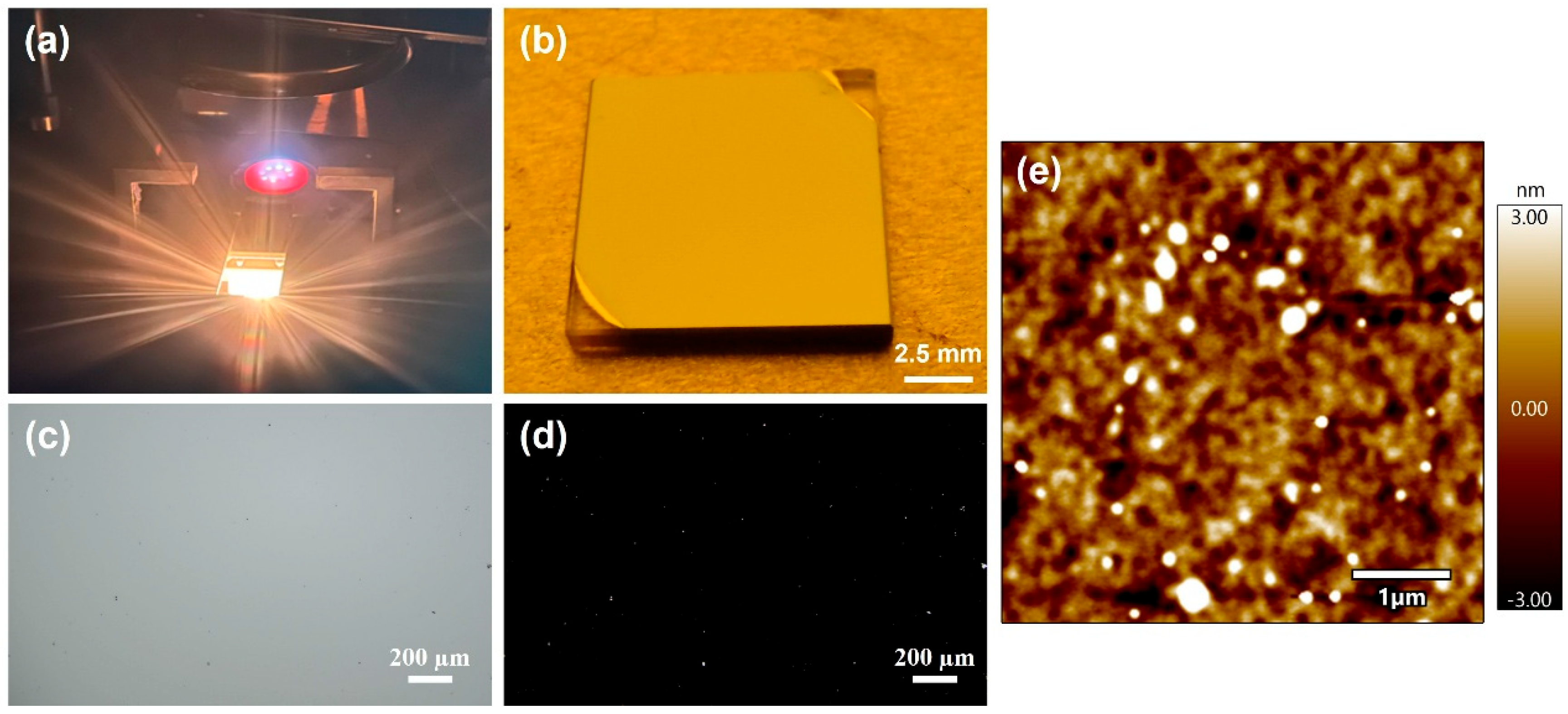
Figure 1: Surface morphology and quality of electron-beam evaporated of As2Se3 films. (a) The evaporation process. (b) As-deposited As2Se3 film with a thickness of ~8 μm on BaF2 substrate. Optical microscope images of the film surface under (c) bright-field (BF) and (d) dark-field (DF) illumination, at 100× magnification. (e) AFM image of 8 μm As2Se3 film.
For thick chalcogenide films used in metalens applications, precise thickness control and uniformity are critical. In this study, we evaluate the controllability and uniformity of electron-beam evaporated As2Se3 films by examining their thickness and composition using SEM and EDS. Fig. 2a–f show cross-sectional SEM images of the films, revealing no observable impurities or structural defects. The measured film thicknesses are 0.53 ± 0.060, 0.97 ± 0.222, 4.05 ± 0.327, 7.93 ± 0.535, 18.6 ± 2.03, and 43.5 ± 1.35 μm, corresponding to deposition times of 3, 5, 15, 30, 70, and 160 min, respectively. Noteworthily, the thickness error represents the variation among different deposition runs. To assess intra-sample uniformity, we measured the thickness along an 8 cm long As2Se3 film deposited in a single run. The thickness was 8.53 μm at the center and 8.29 μm at the edge, yielding a variation of ±0.12 μm relative to the average thickness of 8.41 μm. This small within-run error demonstrates excellent thickness uniformity across the substrate. Given its negligible impact on infrared optical performance, such minor thickness error can be safely disregarded in the context of metalens fabrication.
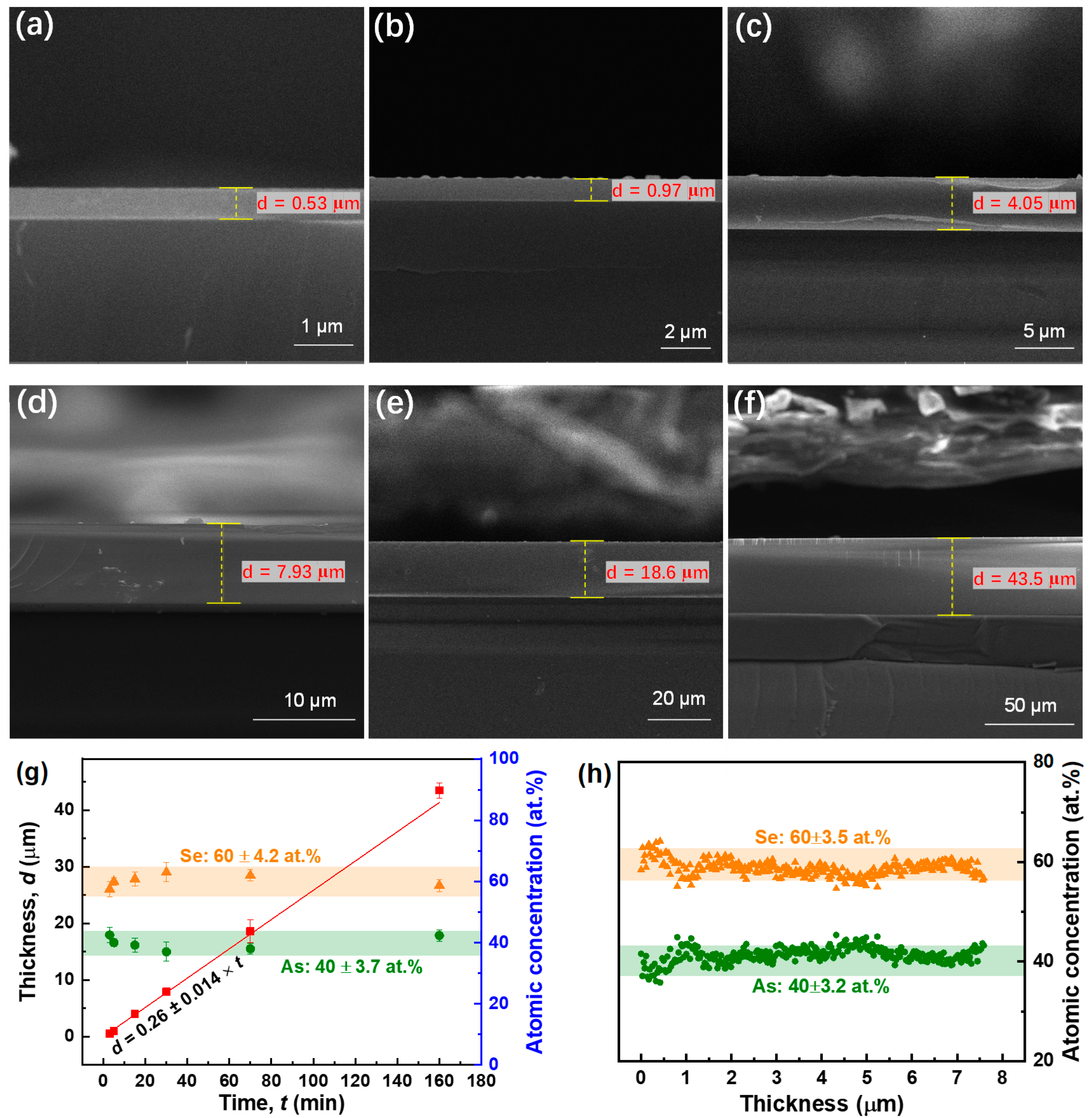
Figure 2: Cross-sectional uniformity and film quality of As2Se3 films. The SEM patterns of cross-section for As2Se3 films obtained by various evaporation time of (a) 3, (b) 5, (c) 15, (d) 330, (e) 70, and (f) 160 min. (g) Time dependent film thickness (left y-axis) and composition (right y-axis) of electron-beam evaporated As2Se3 film. (h) Depth dependent atomic concentration of 8 μm As2Se3 film.
Accordingly, we plotted the film thickness as a function of deposition time, as shown in Fig. 2g (left y-axis). A clear linear relationship is observed between deposition time (t) and film thickness (d), described by d = (0.26 ± 0.014) × t, where d is in micrometers and t in minutes. The coefficient of determination (R2) for this linear fitting is 0.984. This strong linearity demonstrates excellent thickness controllability in the electron-beam evaporation process, with an average deposition rate of 0.26 ± 0.014 μm min−1. To evaluate compositional consistency, EDS was performed on the films deposited at various durations. The atomic concentrations of As and Se, shown in Fig. 2g (right y-axis), reveal a uniform composition across samples, with an average As/Se ratio of 40 ± 3.7/60 ± 4.2, in close agreement with the target stoichiometry of As2Se3. Furthermore, an EDS line scan across the cross-section of a representative thick film (Fig. 2h) shows no significant variation in the As/Se ratio through the depth of the film. The ratio remains consistently near 40/60 throughout, even in films exceeding 8 μm in thickness, indicating excellent compositional uniformity in the vertical direction. Together, these thickness and compositional analyses confirm that electron-beam evaporation enables the fabrication of As2Se3 chalcogenide films with high controllability and exceptional uniformity, key requirements for advanced infrared photonic devices such as metalenses.
High-quality As2Se3 films with excellent thickness controllability and uniformity have been successfully fabricated. However, it remains unclear how the structural and optical properties evolve when bulk As2Se3 is transformed into a thick film via electron-beam evaporation. Fig. 3 presents a comparative analysis of the optical and thermal properties between the bulk glass and the electron beam evaporated As2Se3 film. As shown in Fig. 3a, the bulk sample exhibits a transmittance exceeding 63% across the 1 to 12 μm wavelength range, with a weak absorption peak at ~14 μm attributed to oxidation. In contrast, the transmittance spectrum of the evaporated film displays oscillations due to interference effects arising from its subwavelength thickness. These oscillations range from ~53% to ~93% between 0.7 and 12 μm, yielding an average transmittance of ~73%, significantly higher than that of the bulk. The inset of Fig. 3a presents the Tauc plots used to determine the optical band gaps [27], revealing a difference of approximately 0.2 eV between the As2Se3 film and the bulk material. This widening of the optical band gap is consistent with the observed lower refractive index (n). To quantify this, IR-VASE was performed to determine the wavelength dependent n and extinction coefficient (k). For As2Se3 film sample, we first established an optical model consisting of substrate/film/surface rough layer, which were analyzed with the WVASE32 software package. The thickness of the Si substrate is set to 1 mm, and the thickness of the film sample is determined based on the result measured by SEM. The surface rough layer was defined as 2 nm thick by effective medium approximation (a mixture of 50% film and 50% void). In order to exactly determine the characteristics of the film sample, we used the Tauc-Lorentz oscillation model for data fitting, which is successfully used to simulate the absorption of chalcogenides [28]. For As2Se3 bulk sample, while, a conventional Cauchy model was employed for data fitting. The modeled amplitude ratio (Ψ) and phase difference (Δ) show excellent agreement with experimental data, as illustrated in Fig. 3b, with a low mean squared error (MSE) of 2.387, confirming the reliability of the fitting. The resulting n and k spectra are shown in Fig. 3c. As noted, the extinction coefficient k is defined as the attenuation of transmitted light intensity resulting from both absorption and scattering as light propagates through a material [29]. Thus, the value of k remains very low below ~10 μm indicates high transparency in the mid-infrared, but it increases notably beyond 10 μm, which is in line with the low optical transmittance shown in Fig. 3a. In addition, the refractive index of the film is consistently lower than that of the bulk, by as much as Δn = 0.052 at 8 μm, demonstrating a significant reduction of n in the film sample. This trend is further corroborated by thermal analysis. The DSC traces in Fig. 3d reveal Tg of 170 and 183°C for the film and bulk, respectively, indicating a notable reduction in Tg for the evaporated film. Fig. 3d also reveals a subtle difference in ΔCp between the bulk and film samples. The ΔCp value of the film (2.02 J/(g·°C)) is slightly higher than that of the bulk (1.82 J/(g·°C)), implying a more floppy structure within the film.
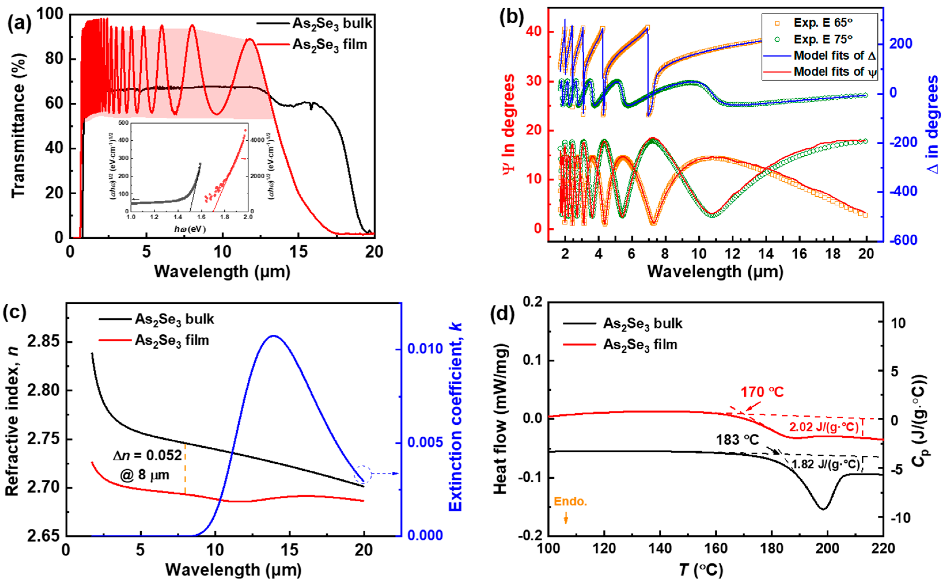
Figure 3: Comparison of properties between bulk As2Se3 and electron-beam evaporated 8 μm thick As2Se3 films. (a) Optical transmittance spectra in the wavelength range of 0.4 to 20 μm. The inset illustrates the difference in optical band gap between the bulk and film samples. (b) Spectroscopic ellipsometry fitting results for the film, showing the Ψ (left y-axis) and Δ (right y-axis) at incident angles of 65° and 75°. (c) Wavelength dependent n and k of the As2Se3 film derived from ellipsometry analysis. (d) DSC traces and heat capacities (Cp) measured at a heating rate of 10 K min−1, showing the Tg and ΔCp of bulk and film samples.
The observed differences in optical transmittance, n, and Tg between As2Se3 films and bulk glass can significantly impact metalens design and fabrication. Therefore, it is essential to investigate the structural origins of these discrepancies. To this end, XRD and Raman spectroscopy were employed. Fig. 4a shows the XRD patterns of the As2Se3 bulk and film. Both exhibit broad halo peaks, confirming their amorphous nature and the presence of a continuous random glass network. However, compared to the bulk, the broad halo peaks of the film are shifted to lower diffraction angles. For instance, the positions of second broad halo peaks are 31.90° for bulk As2Se3 and 30.34° for the electron-beam evaporated film. Using Bragg’s law (λ = 2 × d × sinθ, with λ = 0.154 nm) [30], this shift corresponds to an increase in average interatomic spacing from ~0.505 nm (bulk) to 0.555 nm (film). This indicates a 5% expansion of the atomic network in the evaporated film. This structural modification can be attributed to deposition induced relaxation and altered atomic packing during electron-beam evaporation. In this process, the source material is rapidly vaporized and condenses on the heated substrate. The energetic adatoms possess sufficient surface mobility to reorganize into a more thermodynamically favorable configuration, leading to a more relaxed glass network with reduced internal stress and slightly expanded short- and medium-range order. Specifically, (1) the shift of the first broad peak, associated with the first sharp diffraction peak (FSDP), to lower angles reflects an increase in the average nearest-neighbor distance, suggesting elongated As-Se (or Se-Se) bond lengths or subtle changes in coordination geometry; (2) the shift of the second broad peak, linked to medium-range order, indicates an expansion of structural motifs such as AsSe3 pyramids and Se-Se chains (as further supported by Raman data in Fig. 4b). It may also imply an increase in ring sizes or greater void space between structural units, contributing to a less densely packed and structurally relaxed network.
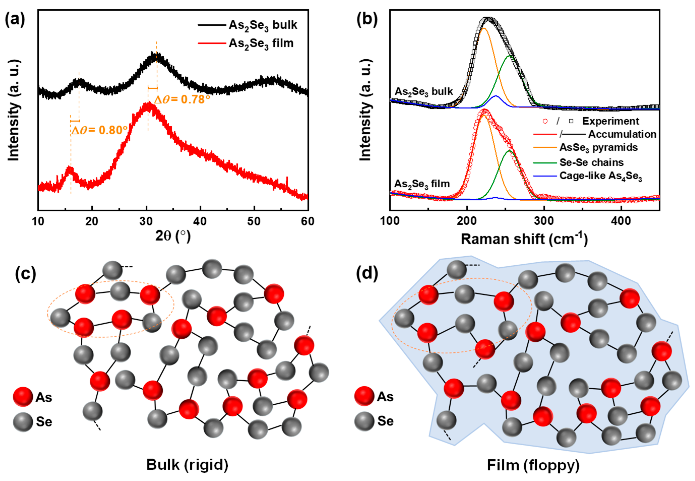
Figure 4: Structural comparison between bulk As2Se3 and electron-beam evaporated As2Se3 films. (a) XRD patterns and (b) raman spectra of the bulk and film samples. The conceptual models depict the As2Se3 glass network in (c) the bulk and (d) the evaporated film. Orange dashed circles highlight the formation and disruption of cage-like As4Se3 units. The shaded region in (d) represents the structurally relaxed network associated with a more flexible, “floppy” structure in the film.
Fig. 4b shows the Raman spectra of the As2Se3 bulk and film. Both exhibit a dominant peak at 222 cm−1 and a shoulder at 255 cm−1, which are assigned to the vibrational modes of AsSe3 pyramids and Se-Se chains, respectively [31]. However, a notable difference is observed at 237 cm−1 (blue curve in Fig. 4b), which is attributed to the presence of cage-like As4Se3 structure [32]. Such structural motifs are typically reported in Se-deficient chalcogenide glasses [32], though small amounts have also been identified in stoichiometric As2Se3 [32,33]. After baseline correction and intensity normalization, the relative contribution of the As4Se3 cage-like Raman mode can be quantified: it accounts for 5.11% of the total spectral area in bulk glass but falls below the detection limit (<1%) in the evaporated film. It is well established that Raman spectroscopy provides relative (not absolute) information about structural motifs, as it is sensitive to local symmetry and polarizability rather than long-range stoichiometry. We acknowledge that the Raman spectra show a distinct As4Se3 signature in the bulk sample but an almost negligible presence in the film. To address this concern and provide quantitative support, we performed peak deconvolution on the Raman spectra. The fitting results reveal that the relative area of the As4Se3 related peak (~237 cm−1) decreases significantly from 5.12% in the bulk glass to 0.87% in the evaporated film. This substantial reduction provides compelling evidence for the structural differences between the bulk and the film, supporting that the As4Se3 cage-like units are nearly absent. Conceptual models of the glass network for bulk and film are shown in Fig. 4c,d, respectively. The yellow dashed circle in Fig. 4c highlights the presence of the cage-like As4Se3 structure in the bulk, which appears to be disrupted or absent in the film (Fig. 4d). This structural transformation may result from the expansion of glass network, as emphasized by the shaded region in Fig. 4d. Compared to the bulk glass, where structural features may be “frozen-in” due to rapid cooling during melt quenching, the film benefits from the controlled condensation process and in-situ thermal effects during electron-beam evaporation (with substrate heating at 120°C in this work). These conditions promote surface mobility and atomic rearrangement, enabling the formation of a more homogeneous and relaxed glass network.
Although the structurally relaxed As2Se3 film offers advantages for infrared applications, such as enhanced optical transmittance and improved long-term environmental stability, it introduces a new challenge, the film-substrate adhesion. It is well known that, the mismatch in thermal expansion coefficients (Δα) between the film and substrate significantly affects the adhesion of heterogeneous films, particularly for thick films subjected to heating or cooling cycles. Table 1 lists the thermal expansion coefficients (α) of various infrared materials, including As2Se3 and common substrate materials. The α of As2Se3 at room temperature is 20.6 × 10⁻⁶°C−1 [34]. We first evaluated the adhesion of thick As2Se3 films (up to 43 μm) deposited on different substrates. As shown in the bright-field optical microscope images in Fig. 5, all films exhibit robust bonding integrity with no visible defects or delamination in the as-deposited state, even at this large thickness. However, after rapid annealing at 120°C for 3 min, cracks emerged in all heterogeneous As2Se3 films except for the As2Se3/BaF2 sample. This indicates a significant adhesion issue in thick As2Se3 films on most substrates under thermal stress, while the As2Se3/BaF2 combination remains robust. The observed cracking is attributed to the large Δα between As2Se3 and the substrate materials, which generates substantial interfacial stress during thermal cycling. We also provide a semi-quantitative estimate of the thermal stress developed during heating, approximated by, σ ≈ E·Δα·ΔT, where E is the Young’s modulus of As2Se3 (~17 GPa) [35], and ΔT = 100°C (from 20°C to 120°C). The calculated thermal stresses in the As2Se3 film are listed in Table 1. The significantly higher stresses induced by Si, Ge, ZnSe, and ZnS, compared to BaF2, may approach or exceed the fracture strength of As2Se3 film, which explains the cracking observed in Fig. 5. In contrast, the much lower stress on BaF2 accounts for its superior mechanical compatibility.
Table 1: Room-temperature coefficient of thermal expansion (α) for various infrared materials, the corresponding thermal expansion mismatch (Δα) between As2Se3 and selected substrates, and the resulting thermal stress (σ) in the As2Se3 film.
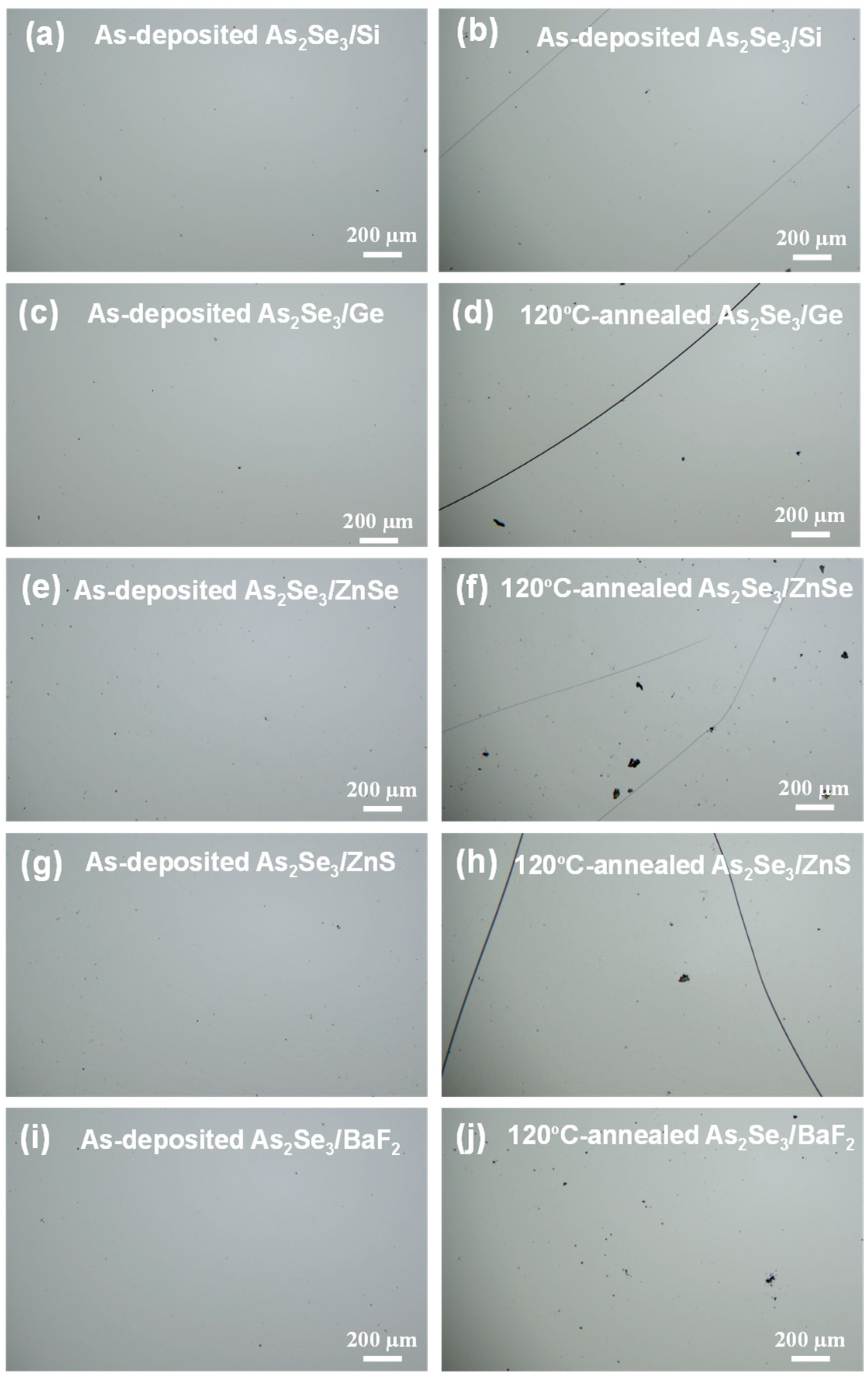
Figure 5: BF optical microscope images of 43 μm thick As2Se3 films deposited on various substrates, before and after annealing, illustrating the degree of thermal expansion mismatch and resulting film integrity. Images were acquired at 100× magnification. The heating step is carried out using a rapid thermal annealing furnace at 120°C with a dwell time of 3 min (heating rate ≈ 40°C s−1). Failure due to adhesion loss is defined as the presence of any visible cracks or delamination observed under optical microscopy.
The Δα between As2Se3 and BaF2 is less than 2.5 × 10⁻⁶°C−1, a value so small that it would seemingly not cause cracking or adhesion failure under normal conditions. However, even such a minor mismatch can lead to interfacial delamination under extreme thermal cycling, particularly during rapid cooling. As illustrated in Fig. 6, we conducted an extreme cooling experiment to evaluate the adhesion of thick As2Se3/BaF2 films. Using a home-built Duvall-type cryogenic chamber rapidly immersed in liquid nitrogen (LN2), we observed numerous cracks in the 43 μm thick As2Se3 film on BaF2 substrate, confirming that even small Δα can induce adhesion failure under severe thermal stress in such thick film. In contrast, no cracks were observed in an 8 μm thick As2Se3/BaF2 film under the same conditions. This indicates that reducing film thickness effectively mitigates thermally induced stress and prevents delamination. To further validate reliability, the 8 μm film was subjected to more than 30 consecutive cycles of rapid heating and extreme cooling. No degradation or adhesion issues were detected, demonstrating the excellent thermal cyclability. Furthermore, as depicted in Fig. 6e, no significant difference can be found in the optical transmittance spectra before and after 30 LN2 quenching cycles. We acknowledge that conventional visible/near-IR metasurfaces use sub-micrometer layers, but far-infrared metalenses (λ = 8–12 μm) fundamentally require multi-micrometer thicknesses to achieve full 2π phase coverage. For As2Se3 film, the thickness of 8 μm satisfies the subwavelength condition (d > λ/n, with n ≈ 2.7). The measured refractive index and high transmittance (~73%) enable full 2π phase coverage with minimal absorption loss, which are the key requirements for efficient single-layer metalenses. Our thickest films (43 μm) were fabricated to explore mechanical limits and enable future stacked or gradient-index devices. These results indicate that the As2Se3/BaF2 system possesses the material prerequisites, such as thermal stability and infrared compatibility, for developing robust heterogeneous metalenses, particularly in extreme environments. However, as this study focuses on material characterization rather than device fabrication, the realization of actual metalens functionality via phase-control structures remains a promising direction for future work.
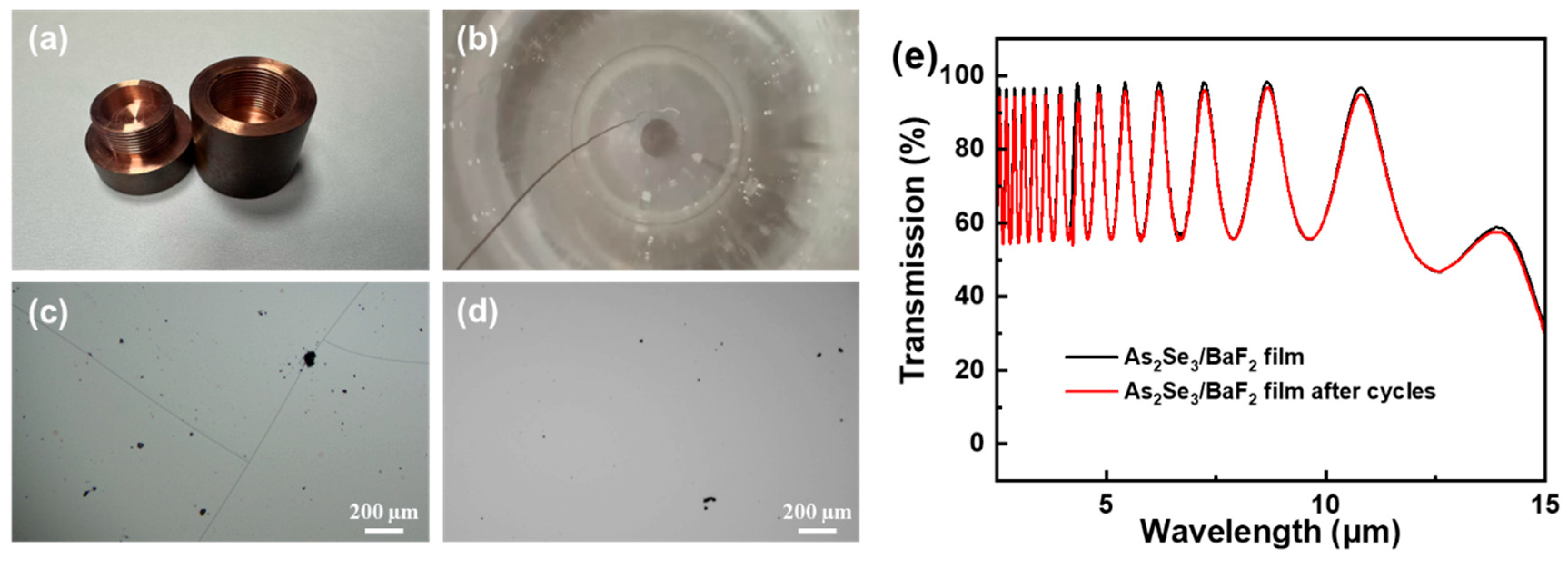
Figure 6: Extreme cooling experiments on As2Se3/BaF2 heterogeneous films, demonstrating their robustness under extreme thermal conditions. (a) A home-built Duvall-type cryogenic chamber used for rapid thermal quenching. (b) Schematic illustration showing the LN2 quenching process. Quenching is achieved by immediate immersion in LN2 (target temperature ≈ −196°C), resulting in a cooling rate of approximately 15°C s−1, followed by a 6 min dwell time at cryogenic temperature. BF optical microscope images of As2Se3/BaF2 films after LN2 quenching with As2Se3 thicknesses of (c) 43 μm and (d) 8 μm. (e) Optical transmittance spectra of 8 μm thick As2Se3 before and after 30 LN2 quenching cycles.
Although the current study demonstrates stability over 30 thermal cycles, which serves as a critical proof-of-concept for the mechanical robustness of the As2Se3/BaF2 interface, it is acknowledged that this does not represent a full-scale accelerated lifetime test. The consistent performance observed in this preliminary reliability evaluation suggests that the system possesses favorable intrinsic stability due to the chemical inertness of the materials and the effective mitigation of thermal stress through heterogeneous integration. Future work will focus on extended cyclic testing (>10,000 cycles) and environmental aging studies to fully characterize the long-term operational lifespan.
In this work, we demonstrate that electron-beam evaporation produces structurally relaxed As2Se3 films with an expanded amorphous network, evidenced by XRD peak shifts and the loss of As4Se3 cage units in Raman spectra, leading to a lower refractive index (~2.7 at 10 μm), high infrared transmittance (~ 73%), and reduced glass transition temperature. While this structural state enhances optical performance for far-infrared meta-optics, it also increases susceptibility to thermal stress. We identify BaF2 as an ideal substrate due to its minimal thermal expansion mismatch (Δα < 2.5 × 10⁻⁶°C−1) and show that an 8 μm thick As2Se3 film, which is sufficient for full 2π phase control in λ = 8–12 μm metalenses, survives over 30 extreme thermal cycles without cracking or delamination. This establishes a critical design paradigm: simultaneous optimization of material structure and geometry enables chalcogenide metasurfaces that are both optically efficient and environmentally robust. The As2Se3/BaF2 platform thus offers a scalable, reliable route toward high-performance infrared meta-optics for real-world applications under harsh thermal conditions.
Acknowledgement:
Funding Statement: This Project is supported by the National Key Research and Development Program of China (Grant No. 2024YFB3815900), the National Natural Science Foundation of China (Grant No. 62374096), and sponsored by K. C. Wong Magna Fund in Ningbo University, China.
Author Contributions: Weihang Qiu: investigation; Bo Zhang: writing—original draft; Zhaofeng Gu: conceptualization, investigation; Zijun Liu: funding acquisition; Xiang Shen: conceptualization, supervision, funding acquisition; Yimin Chen: supervision, investigation, funding acquisition, writing—review & editing. All authors reviewed and approved the final version of the manuscript.
Availability of Data and Materials: The data that support the findings of this study are available from the corresponding authors upon reasonable request.
Ethics Approval: Not applicable.
Conflicts of Interest: The authors declare no conflicts of interest.
References
1. Jeon D , Shin K , Moon SW , Rho J . Recent advancements of metalenses for functional imaging. Nano Converg. 2023; 10( 1): 24. doi:10.1186/s40580-023-00372-8. [Google Scholar] [CrossRef]
2. Wu Y , Wang S . Research on broadband achromatic metalenses. Sci Sin Phys Mech Astron. 2022; 52( 6): 264221. doi:10.1360/sspma-2021-0274. [Google Scholar] [CrossRef]
3. Zhu Y , Yuan G , Chang Y , Zhou S , Wu C , Li Y , et al. Ultra-broadband achromatic metalens with high performance for the entire visible and near-infrared spectrum. Results Phys. 2023; 50: 106591. doi:10.1016/j.rinp.2023.106591. [Google Scholar] [CrossRef]
4. Khorasaninejad M , Zhu AY , Roques-Carmes C , Chen WT , Oh J , Mishra I , et al. Polarization-insensitive metalenses at visible wavelengths. Nano Lett. 2016; 16( 11): 7229– 34. doi:10.1021/acs.nanolett.6b03626. [Google Scholar] [CrossRef]
5. Banerji S , Meem M , Majumder A , Vasquez FG , Sensale-Rodriguez B , Menon R . Imaging with flat optics: Metalenses or diffractive lenses? Optica. 2019; 6( 6): 805. doi:10.1364/optica.6.000805. [Google Scholar] [CrossRef]
6. Sun Z , Han D , Zhang Y . China’s Top 10 optical breakthroughs: Research progress of tunable microlens arrays (invited). Laser Optoelectron Prog. 2024; 61: 1000002. [Google Scholar]
7. Zakery A , Elliott SR . Optical properties and applications of chalcogenide glasses: A review. J Non Cryst Solids. 2003; 330( 1–3): 1– 12. doi:10.1016/j.jnoncrysol.2003.08.064. [Google Scholar] [CrossRef]
8. Robert B , Flaud V , Escalier R , Mehdi A , Vigreux C . XPS study of Ge-Se-Te surfaces functionalized with organosilanes. Appl Surf Sci. 2023; 607: 154921. doi:10.1016/j.apsusc.2022.154921. [Google Scholar] [CrossRef]
9. Hoshino T , Zogg H , Maissen C , Masek J , Blunier S . Fabrication procedures of photovoltaic lead-chalcogenide-on-silicon infrared sensor arrays for thermal imaging. Microelectron Eng. 1991; 15( 1–4): 293– 6. doi:10.1016/0167-9317(91)90232-3. [Google Scholar] [CrossRef]
10. Chen Z , Shu H , Wang X . The latest research development of silicon based integrated optical waveguide amplifier. Sci Sin Phys Mech Astron. 2017; 47( 12): 127301. doi:10.1360/sspma2017-00001. [Google Scholar] [CrossRef]
11. Wen SC , Chang CW , Lin CM , Liu HA , Hsiao VKS , Yu J , et al. Light-induced switching of a chalcogenide-coated side-polished fiber device. Opt Commun. 2015; 334: 110– 4. doi:10.1016/j.optcom.2014.08.033. [Google Scholar] [CrossRef]
12. Helan PPJ , Mohanraj K , Sivakumar G . Thermally evaporated AgyCu2–ySnSe3 metal chalcogenide thin films and its characterization. Opt Mater. 2016; 62: 403– 10. doi:10.1016/j.optmat.2016.10.038. [Google Scholar] [CrossRef]
13. Zhang Y , Li J , Chen Q , Lou S , Zhou S . Magnetron sputtering deposition of MgxGe1−xTe thermoelectric thin films. Sci Sin Phys Mech Astron. 2022; 52: 267311. [Google Scholar]
14. Goglidze TI , Dement’ev IV , Ishimov VM , Senokosov EA . Effect of thermal evaporation rate on the basic physical properties of glassy (As2S3)x(As2Se3)1–x films. Inorg Mater. 2007; 43( 1): 90– 3. doi:10.1134/s0020168507010189. [Google Scholar] [CrossRef]
15. Ogusu K , Hosokawa Y , Maeda S , Minakata M , Li H . Photo-oxidation of As2Se3, Ag–As2Se3, and Cu–As2Se3 chalcogenide films. J Non Cryst Solids. 2005; 351( 37–39): 3132– 8. doi:10.1016/j.jnoncrysol.2005.07.034. [Google Scholar] [CrossRef]
16. Himanshu , Patel SL , Thakur A , Kannan MD , Dhaka MS . Impact of Bi doping on CdTe thin films: Thermal annealing evolution of physical properties for solar cell absorber layer applications. Thin Solid Films. 2020; 709: 138004. doi:10.1016/j.tsf.2020.138004. [Google Scholar] [CrossRef]
17. Kounavis P , Mytilineou E . Formation of a transient disordered state under bias illumination in a-As2Se3. J Non Cryst Solids. 2002; 299–302: 940– 4. doi:10.1016/s0022-3093(01)01057-2. [Google Scholar] [CrossRef]
18. Himanshu , Patel SL , Thakur A , Kannan MD , Dhaka MS . Analysis of different annealing conditions on physical properties of Bi doped CdTe thin films for potential absorber layer in solar cells. Sol Energy. 2020; 199: 772– 81. doi:10.1016/j.solener.2020.02.066. [Google Scholar] [CrossRef]
19. Hossain MI , Mansour S . A critical overview of thin films coating technologies for energy applications. Cogent Eng. 2023; 10( 1): 2179467. doi:10.1080/23311916.2023.2179467. [Google Scholar] [CrossRef]
20. Hossain MI , Chelvanathan P , Aissa B , Khandakar A , Rahman A , Mansour S . Enhanced perovskite solar cells performance with TiOx and SnOx thin films as electron transport layers. Sci Rep. 2025; 15: 7709. doi:10.1038/s41598-024-83600-3. [Google Scholar] [CrossRef]
21. Hossain MI , Aissa B , Khandakar A , Thomas K , Rahman A , Mansour S . Exploring the optical and morphological properties of metal oxide thin films produced via reactive electron beam evaporation. Cogent Eng. 2024; 11( 1): 2338144. doi:10.1080/23311916.2024.2338144. [Google Scholar] [CrossRef]
22. Hossain MI , Khandakar A , Chowdhury MEH , Ahmed S , Nauman MM , Aïssa B . Numerical and experimental investigation of infrared optical filter based on metal oxide thin films for temperature mitigation in photovoltaics. J Electron Mater. 2022; 51( 1): 179– 89. doi:10.1007/s11664-021-09269-w. [Google Scholar] [CrossRef]
23. Hossain MI , Al Kubaisi G , Aïssa B , Mansour S . Probing the hydrophilic behaviour of e-beam evaporated silica thin films for PV-soiling application. Mater Sci Technol. 2022; 38( 11): 753– 9. doi:10.1080/02670836.2022.2063526. [Google Scholar] [CrossRef]
24. Jena BJ , Das S , Senapati S , Naik R . Stability of Ag2S/As2Se3 thin films under time dependent laser irradiation and its impact on linear-nonlinear optical properties for optoelectronic applications. Opt Laser Technol. 2023; 164: 109461. doi:10.1016/j.optlastec.2023.109461. [Google Scholar] [CrossRef]
25. Jena BJ , Alagarasan D , Ganesan R , Naik R . Thermal annealing induced linear/nonlinear properties of Ag2S/As2Se3 heterojunction films for optoelectronic applications. Ceram Int. 2023; 49( 16): 27535– 50. doi:10.1016/j.ceramint.2023.06.029. [Google Scholar] [CrossRef]
26. Sahoo D , Naik R . Phase-change-driven tuning of linear and nonlinear optical properties of Te/As2Se3 bilayer thin films for optoelectronic applications. Mater Sci Eng B. 2023; 297: 116750. doi:10.1016/j.mseb.2023.116750. [Google Scholar] [CrossRef]
27. Wang G , Nie Q , Barj M , Wang X , Dai S , Shen X , et al. Compositional dependence of the optical properties of novel Ge–Ga–Te–CsI far infrared transmitting chalcohalide glasses system. J Phys Chem Solids. 2011; 72( 1): 5– 9. doi:10.1016/j.jpcs.2010.10.018. [Google Scholar] [CrossRef]
28. Chen Q , Wang G , Liu Z , Gao Y , Gu C , Xu T , et al. Optimizing large optical contrast in Ge-Se-Te films via high-throughput method. Prog Nat Sci Mater Int. 2025; 35( 1): 222– 8. doi:10.1016/j.pnsc.2024.12.012. [Google Scholar] [CrossRef]
29. Parida A , Sahoo D , Alagarasan D , Vardhrajperumal S , Ganesan R , Naik R . Increase in nonlinear susceptibility and refractive index in quaternary In15Sb10S15Se60 thin films upon annealing at different temperature for photonic applications. J Alloys Compd. 2022; 905: 164143. doi:10.1016/j.jallcom.2022.164143. [Google Scholar] [CrossRef]
30. Ali A , Chiang YW , Santos RM . X-ray diffraction techniques for mineral characterization: A review for engineers of the fundamentals, applications, and research directions. Minerals. 2022; 12( 2): 205. doi:10.3390/min12020205. [Google Scholar] [CrossRef]
31. Azhniuk Y , Dzhagan V , Solonenko D , Loya V , Grytsyshche I , Lopushansky V , et al. In-doped As2Se3 thin films studied by Raman and X-ray photoelectron spectroscopies. Appl Surf Sci. 2019; 471: 943– 9. doi:10.1016/j.apsusc.2018.12.097. [Google Scholar] [CrossRef]
32. Yang G , Bureau B , Rouxel T , Gueguen Y , Gulbiten O , Roiland C , et al. Correlation between structure and physical properties of chalcogenide glasses in the AsxSe1–x system. Phys Rev B. 2010; 82( 19): 195206. doi:10.1103/physrevb.82.195206. [Google Scholar] [CrossRef]
33. Kovanda V , Vlček M , Jain H . Structure of As–Se and As–P–Se glasses studied by Raman spectroscopy. J Non Cryst Solids. 2003; 326–327: 88– 92. doi:10.1016/s0022-3093(03)00383-1. [Google Scholar] [CrossRef]
34. Musgraves JD , Danto S , Richardson K . Thermal properties of chalcogenide glasses. In: Chalcogenide Glasses. Amsterdam, The Netherlands: Elsevier; 2014. p. 82– 112. doi:10.1533/9780857093561.1.82. [Google Scholar] [CrossRef]
35. Wang X , Wang J , Ruan H . Ergodicity breaking of an inorganic glass aging near Tg probed by elasticity relaxation. Phys Rev B. 2023; 107( 2): 024205. doi:10.1103/physrevb.107.024205. [Google Scholar] [CrossRef]
36. Zhernov AP . Lattice constant and coefficient of linear thermal expansion of the silicon crystal. Influence of isotopic composition. Low Temp Phys. 2000; 26( 12): 908– 15. doi:10.1063/1.1334443. [Google Scholar] [CrossRef]
37. Ma Y , Tse JS . Ab initio determination of crystal lattice constants and thermal expansion for germanium isotopes. Solid State Commun. 2007; 143( 3): 161– 5. doi:10.1016/j.ssc.2007.04.043. [Google Scholar] [CrossRef]
38. Kumar V , Sastry BSR . Thermal expansion coefficient of binary semiconductors. Cryst Res Technol. 2001; 36( 6): 565– 9. doi:10.1002/1521-4079(200107)36:6<565::aid-crat565>3.0.co;2-f. [Google Scholar] [CrossRef]
39. Harris DC . Materials for infrared windows and domes: Properties and performance. 2nd ed. Bellingham, WA, USA: SPIE; 2024. doi:10.1117/3.100006. [Google Scholar] [CrossRef]
Cite This Article
 Copyright © 2026 The Author(s). Published by Tech Science Press.
This work is licensed under a Creative Commons Attribution 4.0 International License , which permits unrestricted use, distribution, and reproduction in any medium, provided the original work is properly cited.
 Downloads
 Citation Tools
