
 Submit a Paper
 Propose a Special lssue
 Open Access
ARTICLE

A Deep Learning- and AI-Enhanced Telecentric Vision Framework for Automated Imaging-to-CAD Reconstruction
1 Department of Information and Computer Sciences, Faculty of Information Technology, Kanagawa Institute of Technology, Kanagawa, Tokyo, Japan
2 Department of Mechanical Engineering, Faculty of Engineering, Chulalongkorn University, Bangkok, Thailand
* Corresponding Author: Ratchatin Chancharoen. Email:
Computer Modeling in Engineering & Sciences 2026, 146(3), 33 https://doi.org/10.32604/cmes.2026.077356
Received 08 December 2025; Accepted 06 February 2026; Issue published 30 March 2026
 View Full Text
 Download PDF
Abstract
This paper presents an automated imaging-to-CAD reconstruction system that combines telecentric vision and deep learning for high-accuracy digital reconstruction of printed circuit boards (PCBs). The framework integrates a telecentric camera with a Cartesian scanning platform to capture distortion-free, high-resolution PCB images, which are stitched into a single orthographic composite. A YOLO-based detection model, trained on a dataset of 270 PCB images across 23 component classes with data augmentation, identifies and localizes electronic components with a mean average precision of 0.932. Detected components are automatically matched to corresponding 3D CAD models from a part library and assembled within a Fusion 360 environment, producing a 3D digital replica. Experimental results show a similarity score of 0.894 and dimensional deviations below 2%, outperforming both SensoPart image measurement and manual vernier methods. The proposed approach bridges optical metrology and CAD automation, providing a scalable solution for AI-assisted reverse engineering, digital archiving, and intelligent manufacturing.Keywords
Nomenclature
| Vector of image pixel coordinates | |
| Vector of world coordinate | |
| Scale factor for converting between image and world units | |
| Translational displacement of the camera or part along the X and Y axes, respectively | |
| Width and height of the detected component i’s bounding box in pixels and in metric units, respectively | |
| Homography matrix | |
| Placement transform, translational placement, and rotation matrix of component i in homogeneous coordinates (rigid body transformation) | |
| Detected component information in metric space and pixel space | |
| Detected class label or component type | |
| Coordinates of component i in the assembly space | |
| Nominal height of component i, estimated from class library or datasheet | |
| rotation angle of component | |
| Assembly information for component i, containing its class type and pose |
The convergence of artificial intelligence (AI), computer vision, and digital manufacturing [1] has profoundly transformed the landscape of industrial inspection and reverse engineering [2,3]. In particular, the ability to reconstruct physical objects into precise three-dimensional (3D) computer-aided design (CAD) models [1,4–6] has emerged as a cornerstone of modern engineering workflows. Such reconstruction not only enables seamless interaction between the physical and digital domains [7] but also facilitates product redesign [2,3], documentation, and digital twin creation [1,8,9], which are integral to Industry 4.0 ecosystems [1,8]. Despite significant advances in image-based modeling, the reconstruction of printed circuit boards (PCBs) [10,11]—planar assemblies characterized by intricate component diversity and fine-scale geometric features—remains a formidable challenge [12–15].
Traditional PCB measurement and documentation approaches have relied heavily on manual metrology and 2D image-based inspection [16]. Techniques such as vernier caliper measurement or coordinate measuring machines (CMMs) [17,18] yield high accuracy but are time-intensive, laborious, and prone to operator-dependent errors. Moreover, they do not produce digital models directly, necessitating additional CAD modeling steps that hinder automation and scalability [5]. Similarly, conventional computer vision methods, including photogrammetry and multi-view stereo, depend on surface texture and perspective variation to infer geometry [14,16,19]. These techniques, however, exhibit limited performance on flat reflective surfaces, where specular reflections and uniform textures obstruct robust feature extraction and depth estimation [20].
Industrial vision systems such as SensoPart offer non-contact, high-speed dimensional analysis but remain fundamentally constrained to two-dimensional feature extraction [21]. Their measurement accuracy is sensitive to lens distortion, illumination uniformity, and calibration stability [22,23]. While valuable for inspection, such systems cannot produce standardized 3D CAD outputs [5,7,24], limiting their suitability for integration with digital design workflows or automated reconstruction pipelines [4].
These challenges collectively delineate a research gap between geometric precision and semantic automation [6,25]. Existing techniques typically achieve one at the expense of the other—either focusing on precise dimensional measurement without object recognition or emphasizing object detection without accurate geometric recovery [6,14,25]. There remains a need for a unified framework that integrates telecentric optical metrology [26], AI-driven component recognition, and CAD-level digital reconstruction [7]. Such a system should not only extract accurate dimensions from distortion-free imagery but also identify, classify, and digitally rebuild each component into a design-ready 3D CAD assembly [4,5,7,27].
In response to this challenge, this study proposes an automated imaging-to-CAD reconstruction framework that fuses telecentric vision, deep learning [28–30], and AI-driven model retrieval [4]. The system employs a high-resolution telecentric camera to capture orthographic, distortion-free PCB images [10,11,28,31], ensuring metrological accuracy across the entire field of view. A YOLO-based deep learning model [19,24], trained on a curated dataset of PCB images [31,32], is utilized to detect and classify components [33–35]. Each detected component is then automatically linked to an online 3D model library or manufacturer datasheet, leveraging internet-based model search and retrieval to reconstruct standardized geometries [14,24]. Finally, the Fusion 360 API automates CAD assembly generation [5], producing a fully parameterized digital twin that faithfully replicates the physical board’s structure and layout [24,36].
The overall concept of the proposed system is illustrated in Fig. 1. Beginning with a physical PCB specimen (in this case, a motor driver board), an orthographic image is captured using the telecentric imaging stage. This image is processed through a fully automated digital workflow comprising component identification, model mapping, and CAD integration [7]. The reconstructed assembly provides an accurate digital equivalent of the physical object, effectively bridging the gap between tangible hardware and virtual design.
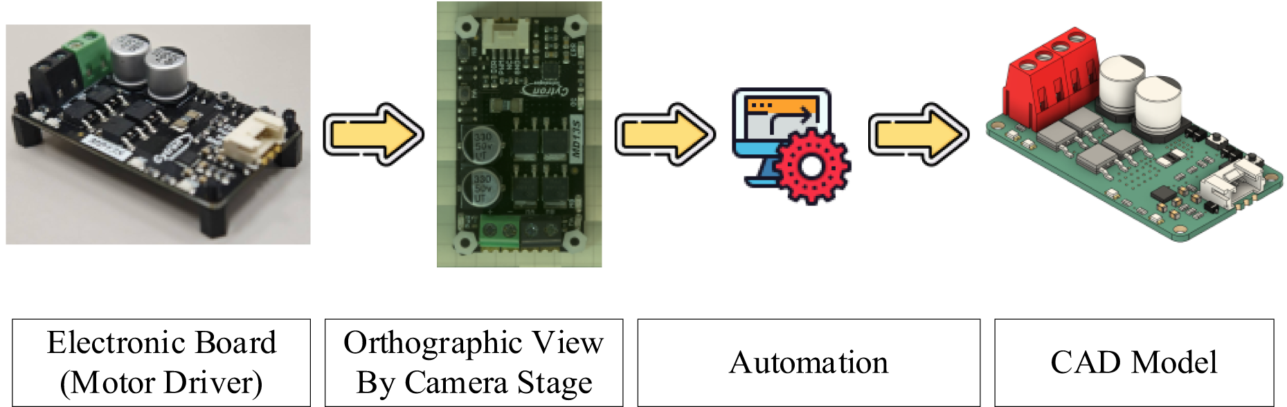
Figure 1: Overview of the automated imaging-to-CAD reconstruction framework.
The key contributions of this study can be summarized as follows:
• Development of an AI-driven imaging-to-CAD reconstruction pipeline integrating telecentric imaging, deep learning–based detection, and CAD automation.
• Implementation of a YOLO-based component recognition model trained on a specialized PCB dataset for robust multi-class identification and localization.
• Establishment of a 3D model library mapping mechanism linking detected components to standardized geometries retrieved from online repositories or datasheets.
• Validation of reconstruction fidelity through quantitative similarity verification, achieving a similarity score of 0.894 and dimensional deviation below 2% relative to manual measurements.
• Comparative evaluation against both industrial vision (SensoPart) and manual methods, demonstrating superior accuracy, automation, and design interoperability.
In summary, this research advances the state of the art by establishing a digital workflow that unites optical metrology and AI-based model retrieval. By enabling automated, high-fidelity, and semantically informed reconstruction of PCBs, the proposed framework lays the foundation for AI-assisted reverse engineering, digital archiving, and smart manufacturing within next-generation Industry 4.0 environments.
2 System Architecture and Hardware Framework
The overall architecture of the proposed automated imaging-to-CAD reconstruction framework is designed to establish a seamless link between optical imaging [16,37], AI-based component recognition [12], and digital CAD generation [5]. As shown in Fig. 2, the system comprises an integrated hardware and software pipeline that enables distortion-free image acquisition, intelligent data interpretation, and fully automated model reconstruction [4]. The framework is structured to ensure that each subsystem—from imaging to computation—contributes to metrological precision and repeatable automation.
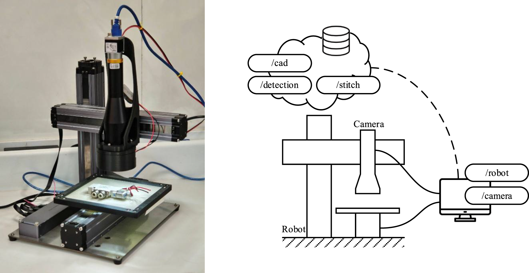
Figure 2: Telecentric camera stage and cartesian robotic imaging hardware.
The hardware configuration of the proposed system is centered on a telecentric imaging stage integrated with a Cartesian robotic platform, designed to ensure precision, repeatability, and scalability in the image acquisition process. This configuration enables accurate and repeatable motion across the X–Y plane, allowing complete visual coverage of the printed circuit board (PCB) under inspection. The robotic platform is governed by a microcontroller-based motion controller running 3D printer firmware equipped with a Controller Area Network (CAN) bus interface, which facilitates distributed control and modular expansion of system components.
The use of the CAN bus communication protocol provides a robust and flexible interconnection between the robotic actuators, illumination modules, and camera triggering unit. This decentralized communication structure enhances real-time synchronization while allowing individual subsystems to be modified or upgraded with minimal wiring complexity. Such an architecture is particularly advantageous for laboratory or industrial environments where scalability and ease of maintenance are essential considerations.
A high-resolution industrial camera (Basler series) [38] equipped with a telecentric lens serves as the primary imaging sensor [13,39]. The telecentric optical system minimizes perspective distortion and maintains constant magnification throughout the entire field of view, thereby ensuring submillimeter measurement accuracy even for components located near the periphery of the image [26,33]. This property is particularly important for PCBs that contain components of varying heights or dense spatial arrangements [4,24], where small perspective shifts can introduce significant geometric errors.
To achieve optimal image contrast and edge clarity, the imaging setup incorporates a ring-type diffuse illumination system positioned coaxially with the optical axis. This illumination method ensures uniform brightness across the target surface and minimizes specular reflections arising from metallic solder joints or reflective component surfaces. The camera, telecentric lens, and lighting assembly are enclosed within a rigid, vibration-isolated frame, maintaining optical alignment and image stability during repeated scanning operations [21].
An external notebook computer serves as the processing and storage unit for the imaging system. It handles real-time video capture, image preprocessing, and temporary data buffering during scanning. This modular separation of imaging and computation allows flexible integration with higher-level control software, cloud-based data services, or remote processing pipelines.
Furthermore, the system’s modular hardware and networked architecture provide a foundation for future development of custom libraries and service-oriented modules, enabling remote operation, data logging, and AI-assisted calibration. The firmware and hardware structure thus embody an open and extensible framework—supporting the long-term evolution of the imaging platform from a standalone measurement device to a smart, networked subsystem within larger digital manufacturing ecosystems.
2.2 Control and Communication Framework
The imaging platform operates under a modular control architecture. Motion commands and camera triggers are coordinated through a microcontroller interface that communicates with a host computer running the data-processing pipeline. Each scan position is predefined in a calibration routine that maps physical coordinates to image pixels, establishing the spatial reference for subsequent reconstruction.
A dedicated Graphical User Interface (GUI) allows the operator to initiate scans and visualize captured frames. The GUI connects to the imaging node via an internal network (e.g., http://192.168.31.254:5007/), where each capture command executes a synchronized imaging sequence. The acquired images are stored and queued for processing, forming the input dataset for the subsequent stages of image stitching and component detection [36].
The proposed framework unites precision imaging with deep learning and CAD modeling through a unified data flow. The image acquisition subsystem captures and logs optical data in high fidelity, while the processing layer—comprising image stitching [36], YOLO-based object detection, and component mapping—translates raw image data into semantically meaningful entities. These entities, consisting of component type, position, and orientation, serve as the digital foundation for CAD model assignment.
The architecture’s modularity ensures compatibility with both local component libraries and online repositories, enabling scalable deployment across diverse electronic assemblies. The resulting system not only automates the imaging-to-model pipeline but also preserves dimensional traceability throughout the workflow, ensuring that each CAD reconstruction remains both geometrically accurate and digitally verifiable.
In summary, the system architecture integrates mechanical precision [20], optical clarity, and computational intelligence into a cohesive framework. The telecentric camera provides accurate orthographic imaging; the Cartesian robot ensures systematic coverage; the controller manages synchronization; and the software modules enable deep learning inference and CAD automation [28]. Collectively, these components form a digital–physical interface capable of translating real-world hardware into standardized, interoperable 3D CAD representations [5,40]—thereby laying the foundation for intelligent reverse engineering and automated digital manufacturing workflows.
3 Methodology and Process Workflow
The methodology of the proposed imaging-to-CAD reconstruction framework establishes a continuous digital pipeline that transforms high-resolution PCB images into accurate 3D CAD assemblies. This process combines telecentric image acquisition, image stitching, deep learning–based component detection, and automated CAD model generation into a coherent data flow, as summarized in Figs. 3 and 4. The pipeline ensures that each computational stage preserves both dimensional accuracy and semantic integrity, ultimately producing a design-ready digital replica of the physical board.
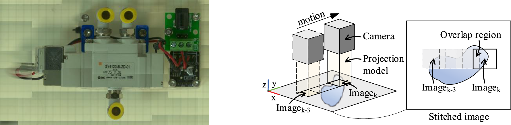
Figure 3: PCB image stitching and orthographic reconstruction workflow.
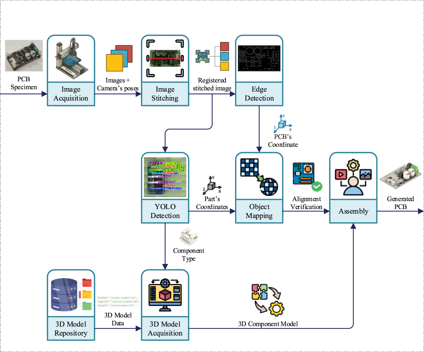
Figure 4: Process flow of the imaging-to-CAD reconstruction pipeline.
3.1 Image Acquisition and Stitching Workflow
The first stage of the process involves capturing multiple telecentric images of the target PCB. Since the telecentric lens provides a limited field of view to maintain optical fidelity, a Cartesian robotic platform performs systematic scanning across the board surface. Each image is captured under identical illumination and exposure conditions to ensure consistent brightness and contrast.
The acquired image set is then processed through an image stitching algorithm that reconstructs a seamless, high-resolution orthographic image of the entire PCB, as illustrated in Fig. 3. The stitching workflow employs feature-based matching and homography [41] transformation to align overlapping regions between adjacent images [36]. A calibration matrix defines the spatial relationship between pixels and physical dimensions (mm), ensuring that the stitched image accurately represents the real-world geometry [36,40].
The relationship between image pixel coordinates u and world coordinates x is described by the homography transformation:
where
Since the telecentric lens is mounted orthogonally to the specimen plane, perspective distortion is negligible, and the homography simplifies to a pure translation transformation:
where
Fig. 3 illustrates the process of multi-position telecentric image acquisition, feature-based alignment, and homography-based stitching used to generate a single high-resolution orthographic image of the PCB. Owing to the telecentric configuration, perspective distortion is minimized and stitching error is constrained primarily to bounded translational misalignment, whose quantitative considerations and impact on downstream detection and reconstruction accuracy are discussed in Section “Quantitative Considerations of Stitching Error”.
Quantitative Considerations of Stitching Error
Image stitching in the proposed framework is performed under a telecentric imaging configuration combined with a Cartesian scanning stage, which significantly constrains geometric distortion and alignment uncertainty. Since the camera motion is restricted to pure planar translation and perspective effects are negligible, the homography used for stitching reduces to a translation model with a fixed scale factor.
Under this configuration, stitching errors are primarily attributed to residual mechanical positioning tolerances of the scanning stage and sub-pixel feature localization uncertainty during image alignment. In practice, these errors remain bounded within a small fraction of a pixel, corresponding to sub-millimeter deviations in the metric domain given the calibrated pixel-to-millimeter scale.
Importantly, the impact of stitching error on downstream component detection and CAD reconstruction is mitigated by the component-level nature of the detection process. Bounding-box localization and class prediction are dominated by local visual features rather than global image alignment. Furthermore, the cumulative influence of stitching error is reflected in the final reconstruction accuracy, where the measured dimensional deviation remains below 2% relative to manual reference measurements, indicating that stitching-induced uncertainty does not significantly affect the overall reconstruction fidelity.
3.2 Component Detection and Classification
Following the construction of the stitched image, a YOLO-based deep learning model is applied to detect and classify PCB components. The model was trained on the training split of a curated dataset of 270 raw PCB images containing 23 component categories, including resistors, capacitors, connectors, and integrated circuits. During inference, the trained model identifies components with their corresponding bounding boxes, class labels, confidence scores, and orientation estimates.
It is worth noting that the learning objective in this work is component-level recognition under a telecentric and illumination-controlled setup, rather than layout-level generalization across arbitrary boards. Since each PCB image contains multiple component instances, the effective number of object-level training samples is substantially larger than the image count. The telecentric configuration also reduces perspective-induced appearance variations, resulting in lower intra-class variability and more stable feature learning.
The reconstruction process requires determining the position and class of each component to assemble the complete digital model. The detection stage provides this information in the form:
where
By applying the known scale factor
where
3.3 Model Mapping and CAD Integration
The next stage involves 3D model assignment and library mapping [37,39,42]. Each detected component class is cross-referenced with a predefined component mapping table that links detection labels to standardized 3D CAD models (STEP files). The retrieved models are then positioned in a virtual environment using the Fusion 360 API, which automates placement according to the converted coordinate data and estimated rotation. This process results in a fully assembled digital model that mirrors the spatial configuration of the physical PCB.
The overall process flow—from image capture to CAD assembly—is summarized in Fig. 4, which highlights the sequential data transformations within the pipeline.
The assembly information for component
where
Under the planar assembly assumption, all components lie on the same reference plane, reducing the full rotation matrix to a single rotation about the
Since the
This framework ensures that each detected part is mapped to a unique 3D pose defined by its class type and planar alignment, enabling automatic placement and assembly of the reconstructed CAD model.
Rotation Angle Estimation and Its Impact on Assembly Precision
In the proposed framework, the rotation angle of each component is estimated as an in-plane orientation during the detection stage and incorporated into the CAD placement transform. Since printed circuit board assemblies are inherently planar, rotational degrees of freedom are restricted to a single axis perpendicular to the board surface, simplifying pose estimation and limiting error propagation.
The rotation angle estimation is derived from the geometric orientation of detected bounding boxes, which provides sufficient angular resolution for component alignment at the assembly level. Small angular deviations primarily affect the orientation of elongated components, while their influence on component centroid placement remains limited. As a result, rotation-related errors manifest as second-order effects in the overall assembly accuracy.
The impact of rotation angle uncertainty is implicitly reflected in the final reconstruction accuracy. As reported in Section 5, the reconstructed CAD models exhibit dimensional deviations below 2% relative to manual reference measurements, indicating that rotation estimation errors do not significantly degrade assembly precision within the defined tolerance. Further refinement of angular estimation and explicit angle error quantification are identified as potential directions for future work.
3.4 Automated Data Management and Workflow Execution
To ensure modularity and scalability, all intermediate data—including image files, detection outputs, and coordinate mappings—are stored in JSON format. This standardized structure allows straightforward exchange of data among subsystems and facilitates post-processing or reconfiguration. The process is fully automated through a Python-based orchestration script that sequentially executes image acquisition, inference, model retrieval, and CAD placement commands.
3.5 Summary of Methodological Advantages
The proposed methodology unifies precision imaging and AI-driven analysis within a digitally traceable workflow. The telecentric imaging stage guarantees geometric reliability; the deep learning model provides semantic interpretation; and the CAD integration stage ensures interoperability with industrial design tools. Together, these stages constitute a fully automated and measurement-consistent digital reconstruction pipeline, forming the backbone of intelligent reverse engineering and digital manufacturing processes.
4 Deep Learning–Based Component Detection and 3D Part Library Mapping
The core of the proposed framework lies in the integration of deep learning–driven perception with knowledge-based 3D model reconstruction. This section outlines the processes of component detection, classification, and library-based model assignment, which collectively enable automated digital assembly generation.
4.1 YOLO-Based Component Detection
A You Only Look Once (YOLO) object-detection model was implemented to perform high-speed and high-accuracy recognition of PCB components. The model was trained on the training split of a custom dataset of 270 high-resolution raw PCB images, with data augmentation applied during training.
During inference, the network outputs bounding boxes, class labels, confidence scores, and orientation estimates for each detected component. As illustrated in Fig. 5, the model consistently identifies diverse component types even within densely populated regions of the board. Quantitative evaluation yielded a mean average precision (mAP@0.5) of 0.932, confirming both the robustness and reliability of the trained detector.
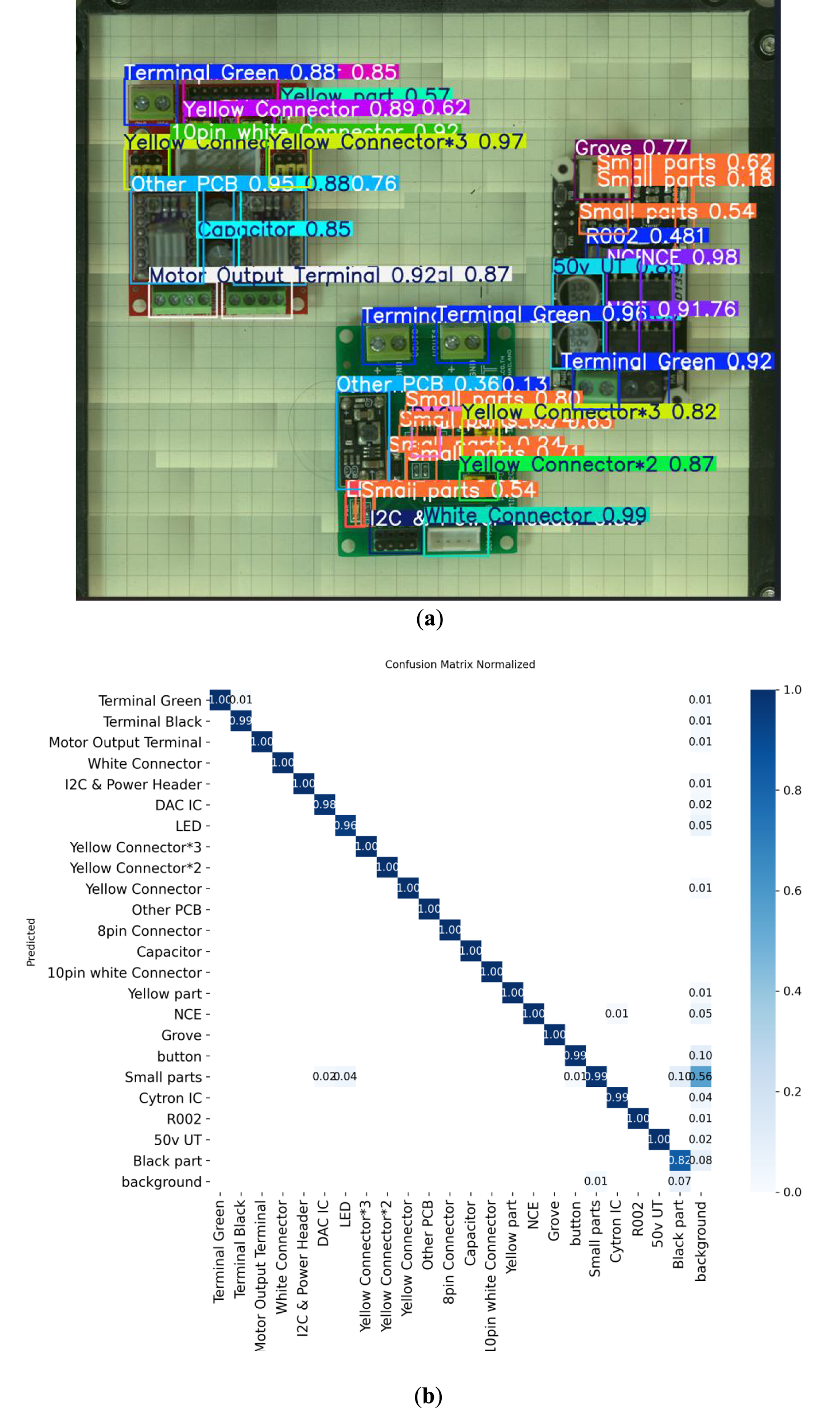
Figure 5: YOLO-based multi-component detection on PCB assemblies: (a) YOLO detection; (b) normalized confusion matrix of YOLO detection model.
4.1.1 Dataset Scope and Generalization Considerations
The dataset used in this study comprises 270 raw PCB images and is sufficient to demonstrate the feasibility and effectiveness of the proposed imaging-to-CAD reconstruction framework under controlled experimental conditions. However, the dataset size limits a full statistical assessment of generalization across highly diverse PCB layouts and manufacturing environments.
Accordingly, the experimental results in this study should be interpreted as evidence of reliable component-level detection performance within the defined imaging setup, rather than as a claim of universal generalization. Expanding the dataset to include a wider range of board designs, component variations, and manufacturing conditions is identified as an important direction for future work.
4.1.2 Implementation Details and Training Configuration
The component detector was implemented using the Ultralytics YOLO framework with the YOLOv8n architecture initialized from pretrained weights (yolov8n.pt). Model training was performed for 100 epochs with an input image size of 640 and a batch size of 8, with built-in augmentation enabled.
To improve generalization under limited data, the training process utilized a dataset of 270 base PCB images, with data augmentation applied during training to generate diverse augmented samples. The augmentation pipeline included (i) geometric transforms (horizontal flipping with probability 0.5, vertical flipping with probability 0.1, shift/scale/rotate with probability 0.5; translation within ±5% of image size, scaling within ±10%, rotation within ±10°; and boundary reflection for edge filling), (ii) photometric variations (brightness and contrast up to ±0.2; hue up to ±15; saturation up to ±20; value up to ±15), and (iii) blur/noise injection (blur_limit = 3; noise dispersion in the range 10.0–50.0). This augmentation strategy was adopted to mitigate overfitting and enhance robustness to realistic variations in positioning, illumination, color tone, blur, and noise.
During inference, a fixed confidence threshold and non-maximum suppression (NMS) were applied to all detection results to suppress false positives, particularly in densely populated PCB regions. These post-processing parameters were kept constant across all experiments, including the evaluation shown in Fig. 5a and the computation of the reported mAP value. No class-specific threshold tuning was performed.
All experiments were conducted on a workstation equipped with an 11th Gen Intel Core i5-1155G7 CPU (2.50 GHz), 16 GB RAM, running Windows 11 Pro. Training and inference were implemented using the Ultralytics YOLO framework with the YOLOv8n model.
4.1.3 Class Imbalance and Class-Level Performance Analysis
The training dataset used in this study contains multiple component categories with inherently different visual frequencies and spatial footprints on typical PCB layouts. As a result, class imbalance is expected at the component level, particularly between frequently occurring passive components and less common specialized parts.
Rather than enforcing explicit class rebalancing strategies, this study evaluates the impact of class imbalance through class-level performance analysis using the normalized confusion matrix shown in Fig. 5b. The results indicate that the majority of component classes achieve high classification accuracy, while misclassifications are primarily concentrated among visually similar or low-contrast categories, such as small components, dark-colored parts, and background-adjacent regions.
These misclassifications are attributed mainly to limited visual distinctiveness and small physical footprints, rather than systematic bias toward majority classes. Importantly, the observed classification behavior does not adversely affect the downstream imaging-to-CAD reconstruction process, as component placement and assembly accuracy remain within the reported dimensional tolerance.
Targeted data augmentation strategies focusing on small or visually similar component classes, as well as class-specific feature refinement, may further improve detection robustness and are identified as promising directions for future work.
4.2 3D Model Assignment and Library Mapping
Following detection, each identified component is mapped to its corresponding 3D geometry through a component-to-library mapping algorithm. This process links the YOLO-derived class label to a standardized STEP model stored in a custom CAD library. The mapping table defines each relationship (e.g., Resistor → resistor_0603.STEP), ensuring consistency in geometric representation and compatibility with commercial CAD software.
The mapping engine automatically searches both local databases and online repositories or manufacturer datasheets, thereby expanding the system’s adaptability and enabling on-demand model retrieval for components not yet stored locally. Dimensional parameters from datasheets—such as package size and pin pitch—are parsed to scale the imported model precisely. The process is summarized in Fig. 6, which illustrates the logical correspondence between detection output and standardized CAD entities.
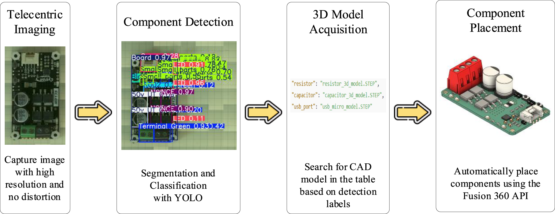
Figure 6: Model assignment and library mapping.
The final stage of the proposed framework involves automated 3D assembly generation through the Fusion 360 API, which serves as the interface between the perception-driven reconstruction process and the digital design environment. In this stage, each detected component is placed within a three-dimensional coordinate space based on its converted spatial coordinates (from pixels to millimeters) and its estimated rotation angle obtained from the detection model. This coordinate transformation ensures that each part is positioned according to its true physical location on the printed circuit board (PCB), thereby preserving geometric fidelity.
The automation script developed for this process manages model importation, spatial alignment, and hierarchical assembly generation. The placement operation follows a transformation protocol that systematically applies translation and rotation matrices derived from the YOLO detection outputs. As a result, all components are accurately oriented and aligned within the reconstructed digital assembly. The output is a dimensionally consistent, parametric CAD model that faithfully represents both the physical structure and component topology of the original PCB.
As illustrated in Fig. 7, the integration workflow transforms a collection of discrete detection results into a coherent digital assembly, demonstrating a seamless transition from optical perception to computer-aided modeling. Beyond reconstruction, the generated assembly can be directly integrated into the Fusion 360 design space, allowing further parametric modification, mechanical analysis, or enclosure design without additional preprocessing.
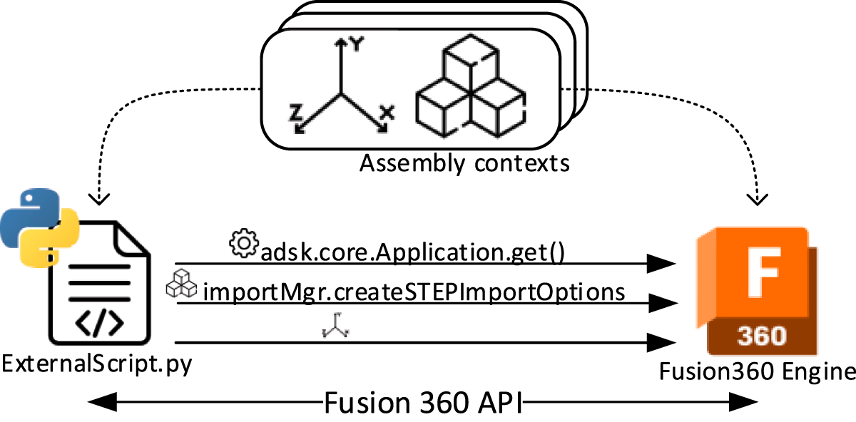
Figure 7: CAD model integration in the fusion 360 environment.
This automated CAD integration stage thus serves as the culmination of the imaging-to-CAD pipeline, bridging computer vision and digital manufacturing. By eliminating manual modeling steps and ensuring data interoperability, it establishes a reproducible pathway for AI-assisted reverse engineering, inspection, and digital twin creation within contemporary design and manufacturing ecosystems.
4.4 Advantages and Implications
The combination of deep learning detection and knowledge-based model mapping offers several key advantages. First, it eliminates manual intervention in component identification, thereby improving reproducibility and reducing reconstruction time. Second, by leveraging online CAD resources and datasheet-driven parameterization, the system remains extensible to new component types. Finally, integration with CAD software ensures interoperability with existing design workflows, enabling direct use of the reconstructed assemblies for reverse engineering, mechanical integration, and digital twin development.
In summary, this stage transforms semantic recognition into tangible geometric representation, forming the bridge between AI-driven perception and CAD-level automation. Together with the imaging and stitching stages, it completes a closed-loop workflow that allows the system to automatically translate raw PCB imagery into an accurate, design-ready 3D model.
5 Accuracy Verification and Comparative Performance Analysis
The accuracy of the proposed imaging-to-CAD reconstruction framework was rigorously evaluated through both visual similarity verification and quantitative dimensional analysis [20]. These evaluations were designed to confirm that the reconstructed digital models preserve the geometric integrity and scale of the corresponding physical PCBs. Figs. 8 and 9 present the comparison methods and results obtained through these validation procedures.
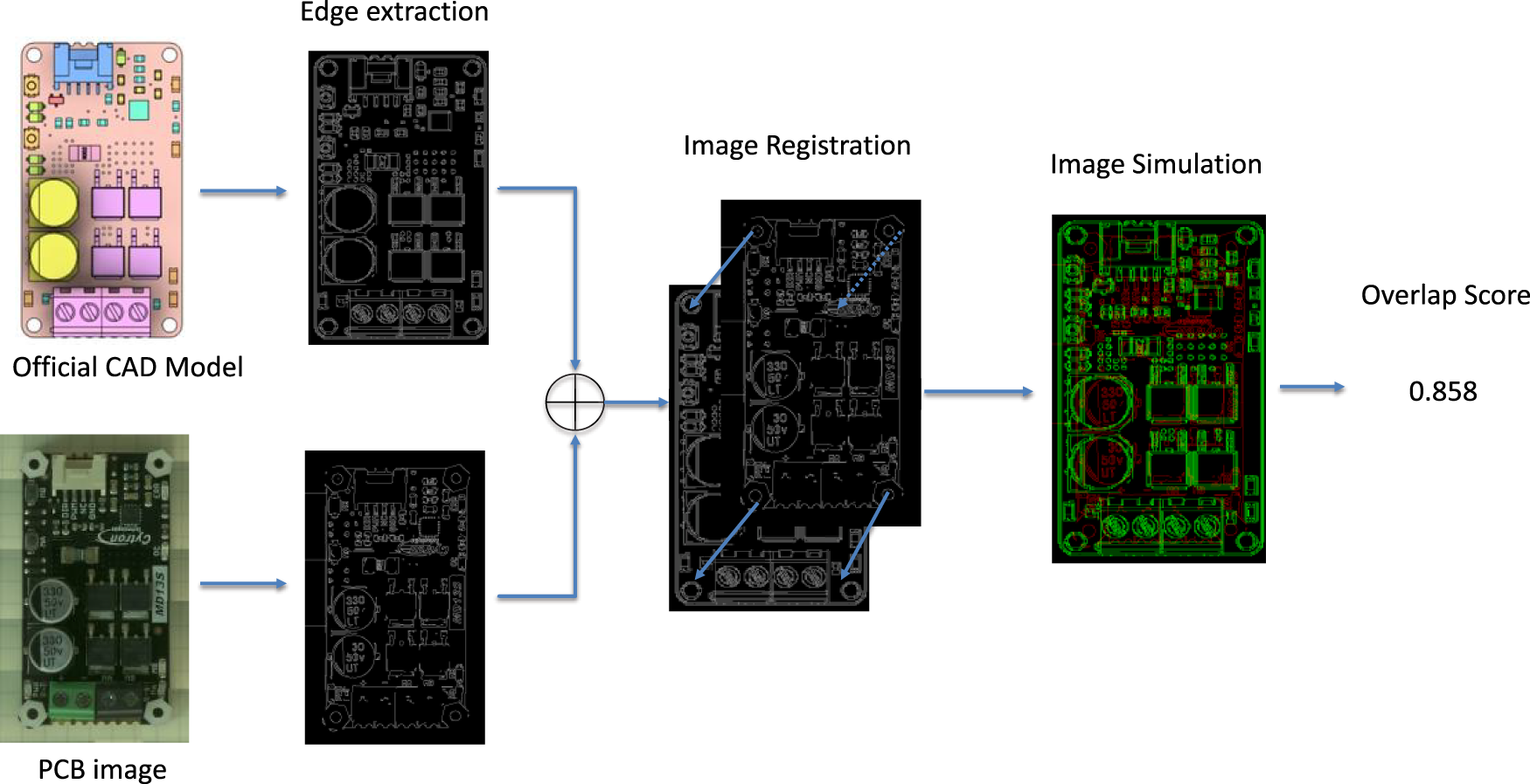
Figure 8: Visual similarity verification between generated CAD and ground-truth PCB.
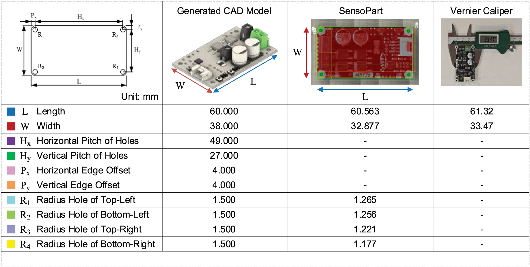
Figure 9: Quantitative similarity verification and statistical accuracy evaluation.
5.1 Method of Similarity Verification
To assess geometric fidelity, a similarity verification method was developed that compares the reconstructed CAD outline against the ground-truth PCB image. The procedure involves extracting the edge contours and component boundaries from both datasets and performing an overlay comparison. The resulting composite image uses a red–green overlay scheme, where overlapping regions appear yellow, signifying accurate correspondence between the reconstructed and actual geometries. Non-overlapping regions are visualized as residual color differences, indicating local deviations.
This visual inspection method enables rapid qualitative assessment of reconstruction performance, highlighting areas of precise alignment as well as minor discrepancies in orientation or placement. The verification confirms that major components, connectors, and board outlines align accurately across both domains.
In the visual similarity verification shown in Fig. 8, edge extraction was applied consistently to both the reconstructed CAD model and the corresponding PCB image using standard gradient-based edge detection parameters. The parameters were selected to balance edge continuity and noise suppression and were kept identical across all evaluated cases to ensure fair comparison.
We observed that moderate variations in edge extraction parameters primarily affect fine edge details but do not significantly alter the overall overlap pattern or the resulting similarity interpretation. As the red–green overlay is intended as a qualitative visualization rather than a standalone quantitative metric, the reported similarity results remain stable within a reasonable parameter range.
5.2 Quantitative Evaluation Metrics
In addition to visual comparison, quantitative similarity metrics were computed to measure reconstruction accuracy. The similarity score (S) was defined as the ratio of overlapping area to the union of the reconstructed and reference outlines, mathematically expressed as:
The proposed method achieved a similarity score of 0.894, indicating that over 89% of the reconstructed geometry accurately matches the real board. Additionally, dimensional deviation analysis revealed an average error below 2% when comparing reconstructed component placements and overall board size against manual vernier measurements. Deviations were primarily localized around small peripheral elements, where sub-pixel localization and angle estimation introduced minor discrepancies.
5.3 Comparative Analysis with Existing Techniques
For benchmarking, the proposed method was compared with two conventional techniques:
• Vision-based image measurement using a SensoPart system, and
• Manual vernier caliper measurement.
While the SensoPart system provided fast, non-contact measurement, it exhibited higher dimensional error due to lens distortion and limited calibration adaptability. Manual measurements offered superior precision but required significant time and human effort, making them unsuitable for scalable applications. The proposed AI-assisted telecentric framework achieved comparable precision to manual methods while offering the speed, repeatability, and automation absent in traditional approaches.
The experimental findings confirm that the proposed framework delivers high geometric fidelity and reproducibility. The combination of telecentric imaging and deep learning detection ensures dimensional accuracy, while the automated model mapping and CAD integration stages eliminate manual intervention. The quantitative verification results substantiate the framework’s suitability for reverse engineering, inspection, and digital archiving—applications where both geometric accuracy and semantic understanding are critical.
Overall, the accuracy verification demonstrates that the proposed imaging-to-CAD pipeline effectively bridges the gap between optical metrology and digital design automation, providing a scalable foundation for intelligent reconstruction in Industry 4.0 environments.
6 Experimental Results and Discussion
The experimental evaluation of the proposed automated imaging-to-CAD reconstruction framework demonstrates its capability to achieve accurate, efficient, and scalable reconstruction of printed circuit boards (PCBs). The results confirm that the integration of telecentric imaging, deep learning detection, and CAD model automation substantially enhances both geometric fidelity and workflow efficiency compared with existing industrial and manual techniques.
The system was tested on multiple PCB samples varying in component density, geometry, and surface characteristics. For each specimen, the reconstruction process successfully produced a complete and dimensionally accurate 3D CAD model that closely matched the physical counterpart. The framework consistently achieved a similarity score of 0.894 and an average dimensional deviation below 2%, indicating a strong correspondence between physical and digital representations.
Processing time for a typical PCB (approximately 80 mm × 60 mm) was approximately 40–45 s, including image acquisition, stitching, detection, and CAD assembly. This represents a significant reduction compared to manual measurement workflows, which typically require 10–15 min per board. These results demonstrate that the proposed method achieves a favorable trade-off between accuracy and computational efficiency, making it suitable for industrial inspection and high-throughput applications.
A comparative analysis was conducted between the proposed system, SensoPart vision-based image processing, and manual vernier measurement. The SensoPart system achieved fast image acquisition but was limited to two-dimensional feature analysis and exhibited measurement deviations of 2%–3% due to optical distortion and calibration dependency. The manual vernier method yielded slightly higher precision but suffered from low repeatability and scalability.
The proposed AI-assisted telecentric system outperformed both techniques, delivering high precision, full automation, and digital interoperability. Its ability to directly output standardized CAD assemblies further distinguishes it from conventional methods, which require additional modeling steps before integration with design workflows.
6.3 Generalization and Robustness
The generalization analysis presented in this section is based on evaluations conducted on PCB layouts and heterogeneous electromechanical assemblies that were not included in the training dataset. All experiments were performed using the same trained detection model and identical inference settings, including confidence thresholds and non-maximum suppression parameters, without any retraining or fine-tuning. The results shown in Fig. 10 therefore provide qualitative evidence of cross-layout and cross-domain applicability of the proposed framework. Owing to the limited dataset size, these observations are not intended to support broad statistical generalization claims, but rather to demonstrate robustness under unseen configurations.
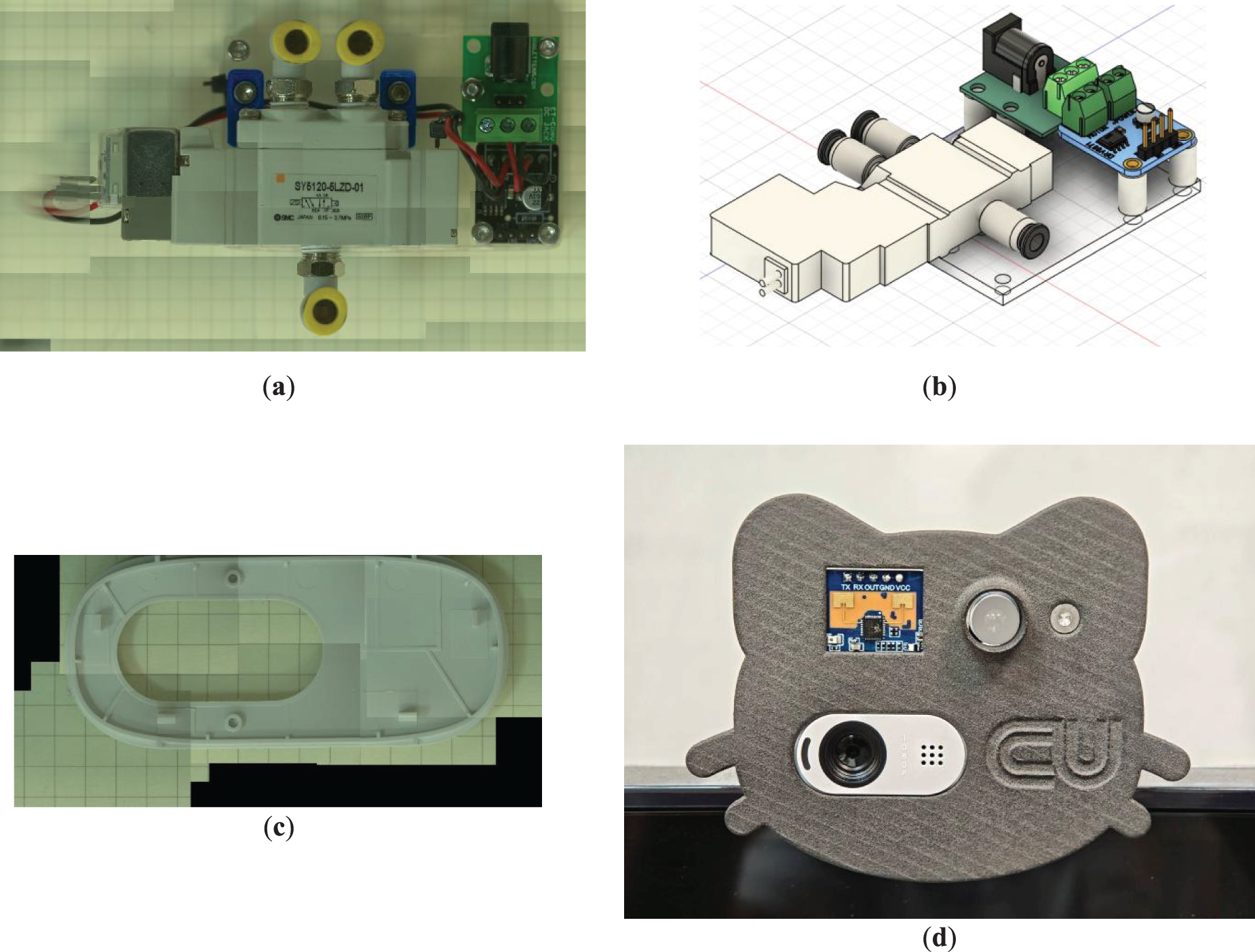
Figure 10: Demonstration of the proposed framework on diverse cases. (a) Industrial solenoid valve, (b) DRV8871 motor driver, (c) DC-jack case, (d) Product assemble.
The generalization capability of the proposed framework was assessed by applying the complete reconstruction pipeline to a variety of PCB configurations not included in the original training dataset. As illustrated in Fig. 10, the system successfully reconstructed multiple board types—including motor driver circuits, sensor modules, and power conversion units—without requiring retraining, recalibration, or parameter adjustments. This outcome indicates that the framework demonstrates a high level of robustness to variations in component density, board topology, and electrical layout.
The deep learning model maintained reliable detection performance across surfaces exhibiting considerable variation in reflectivity, color contrast, and texture. This observation suggests that the trained detector generalizes effectively to real-world imaging conditions, where solder joint gloss, component coatings, or silkscreen inconsistencies frequently undermine the performance of traditional computer vision algorithms. The telecentric imaging configuration further enhanced this robustness by providing distortion-free and illumination-stable imagery, thereby reducing feature loss and minimizing uncertainty in component localization.
To examine cross-domain applicability, the framework was further extended to reconstruct a pneumatic solenoid valve assembly interfaced with a microcontroller (also shown in Fig. 5). High-resolution images of the electromechanical assembly were captured using the proposed hardware, after which the detection pipeline identified key elements—including Fig. 10a, an industrial solenoid valve with CAD models available through both SMC’s hardware library and the Fusion 360 component repository, Figs. 10b, a DRV8871 motor driver commonly used in Arduino-based robotic systems, and Figs. 10c, a DC-jack case breakout module sourced from a Thai supplier. These components were automatically retrieved from the appropriate CAD libraries and placed within a unified CAD environment, demonstrating that the workflow generalizes effectively to mixed mechanical–electronic assemblies.
All results shown in Fig. 10 were obtained using the same trained detection model, component mapping strategy, and calibration settings as those used for PCB reconstruction, without any model retraining, parameter adjustment, or library restructuring.
A further use case involved the reconstruction of the Logitech B100 camera chassis, which served as a platform for integrating a millimeter-wave sensor and an LED illumination module. As no publicly available CAD models or dimensional specifications exist for this camera enclosure, the proposed imaging and reconstruction pipeline was employed to digitize the outer cover and its mounting features. The resulting CAD geometry enabled the design of a precise mounting interface for the sensor and LED module, illustrating the value of the method in product customization and accessory design.
Taken together, these results demonstrate that the proposed framework exhibits strong robustness, cross-domain adaptability, and practical utility across heterogeneous hardware scenarios. Its ability to handle diverse PCBs, electromechanical assemblies, and consumer electronic housings underscores its potential for deployment in digital archiving, automated inspection, custom hardware design, and AI-assisted reverse engineering across a broad spectrum of industrial applications.
6.4 Failure Case and Error Propagation Analysis
While the proposed framework demonstrates strong average performance, certain failure cases were observed under challenging imaging and component conditions. Analysis of the normalized confusion matrix in Fig. 5b indicates that misclassifications primarily occur among visually similar or low-contrast component categories, such as small-sized passive components, dark-colored parts, and components located near background boundaries.
Additional failure cases arise when components exhibit minimal geometric asymmetry, limiting the reliability of in-plane rotation estimation. In such cases, angular ambiguity may occur, although its impact on downstream CAD assembly remains limited due to the planar nature of PCB layouts and the tolerance of component placement in the reconstructed models.
Challenging surface conditions, including strong solder joint reflections, uneven silkscreen printing, and low color contrast between components and the substrate, may also degrade detection confidence. Nevertheless, the telecentric and illumination-controlled imaging setup mitigates many of these effects by reducing perspective distortion and stabilizing visual appearance.
Importantly, the observed failure cases do not significantly affect the overall reconstruction accuracy. As reflected in the reported dimensional deviation below 2%, local detection or orientation errors are typically absorbed within the assembly tolerance of the CAD reconstruction process. Addressing these failure modes through expanded datasets, improved angular estimation strategies, and adaptive training remains an important direction for future work.
6.4.1 Qualitative Analysis of Detection Failure Cases
To provide a clearer interpretation of detection behavior in practical scenarios, a qualitative comparison of representative detection outcomes is presented in Fig. 11. This comparison aims to illustrate how detection performance influences the downstream reconstruction process at the component level.
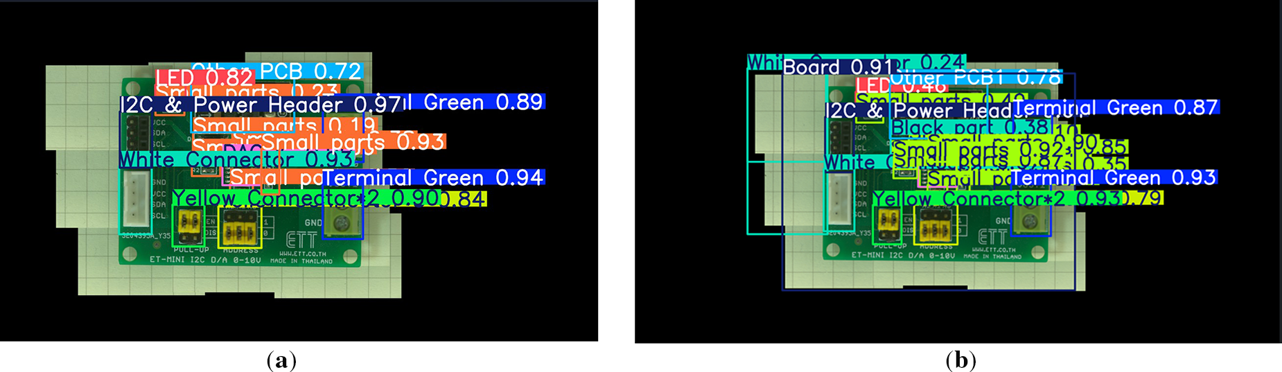
Figure 11: Example of detection: (a) correct detection case, (b) false detection case.
Fig. 11a demonstrates a successful detection case in which the target component is correctly localized and classified. The bounding box accurately encloses the component region, allowing reliable centroid estimation and orientation extraction. Consequently, the metric conversion stage produces accurate positional information, and the corresponding CAD model is correctly retrieved and placed within the assembly. This case represents the ideal pipeline behavior, where visual recognition directly translates into geometrically consistent reconstruction.
In contrast, Fig. 11b illustrates a representative false detection scenario. In this case, a background region is incorrectly identified as a component candidate. This type of error typically occurs when background patterns exhibit visual characteristics similar to certain component textures or intensity distributions. The incorrect detection leads to the assignment of an unintended component class and the retrieval of an inappropriate CAD model during the library mapping stage.
From a reconstruction perspective, such detection errors may propagate into two primary effects. First, incorrect component classification can introduce semantic inconsistencies in the assembled CAD model. Second, bounding box misplacement may cause centroid estimation offsets, resulting in localized positional deviations. However, because PCB assemblies are predominantly planar and components are placed within predefined layout constraints, these localized errors generally remain spatially confined and do not significantly distort the global board geometry.
The qualitative comparison highlights that most detection failures originate from localized visual ambiguity rather than systematic model instability. This observation supports the robustness of the proposed reconstruction framework, while also suggesting that detection reliability can be further improved through enhanced background discrimination, expanded negative training samples, and refined feature representation for visually subtle components.
6.4.2 Error Propagation from Detection to CAD Reconstruction
To illustrate how perception inaccuracies influence the reconstruction process, Fig. 12 presents a schematic representation of error propagation from object detection to CAD assembly generation. Detection errors may arise from incorrect classification, bounding box misalignment, or orientation estimation uncertainty.
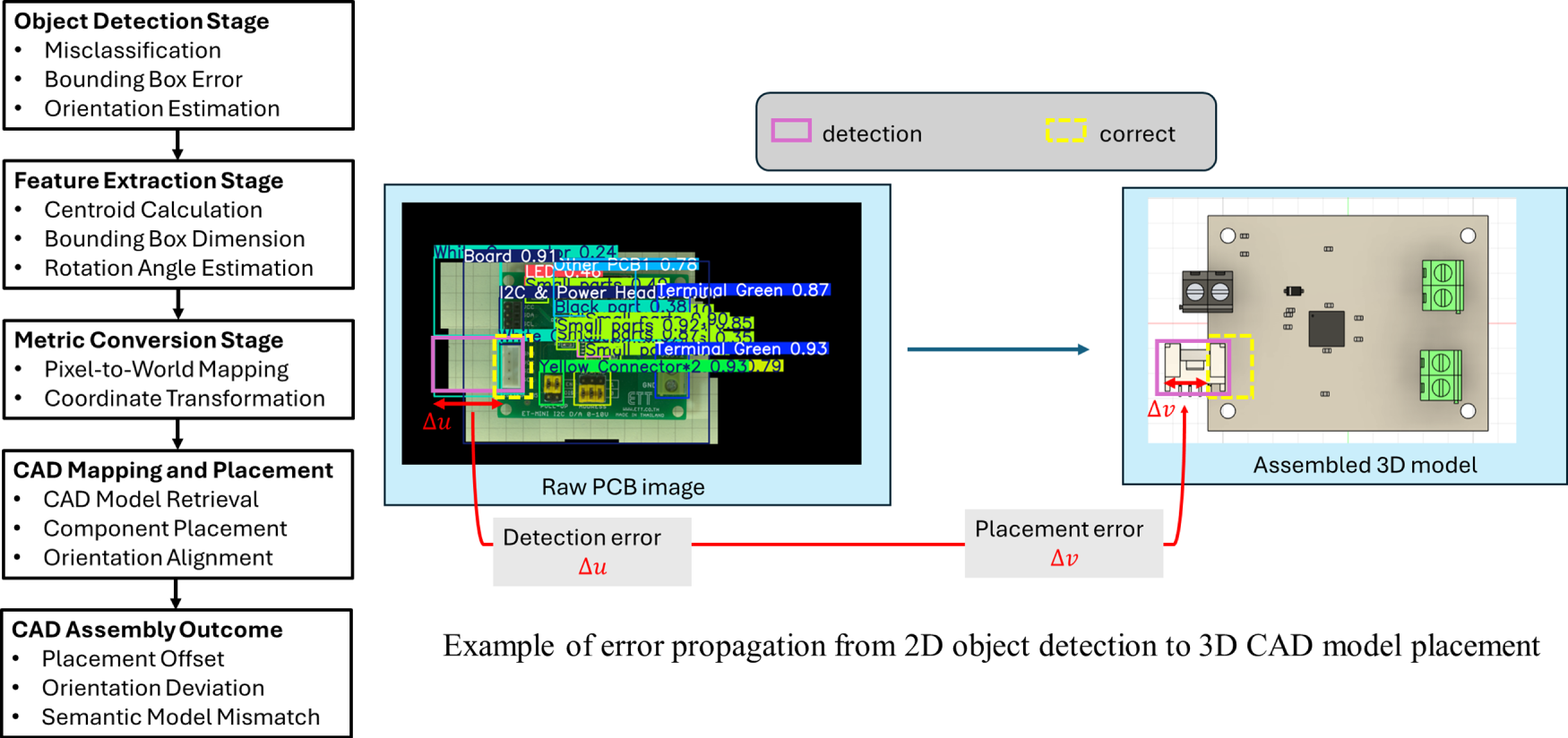
Figure 12: Schematic representation of error propagation from object detection inaccuracies to CAD reconstruction deviations, illustrating how detection errors influence feature extraction, metric coordinate conversion, and final assembly placement.
Bounding box inaccuracies may lead to centroid displacement during metric conversion, resulting in localized positional offsets in the CAD assembly. Similarly, orientation estimation errors may introduce angular misalignment, particularly for direction-sensitive components. Misclassification errors may also cause the retrieval of incorrect CAD models, leading to geometric or semantic inconsistencies in the reconstructed design.
Despite these potential error pathways, the overall reconstruction framework remains robust. PCB assemblies are inherently planar and follow predefined layout constraints, which limit the spatial influence of localized detection errors. This behavior is consistent with the quantitative evaluation results, where dimensional deviations remain below 2%. The propagation model therefore provides an engineering interpretation of how detection reliability affects downstream reconstruction performance.
The results suggest that the proposed framework can significantly accelerate digital documentation, quality inspection, and design modification processes in electronics manufacturing. By enabling direct transition from physical hardware to digital CAD environments, the system facilitates downstream activities such as enclosure design, thermal simulation, and digital twin creation. Furthermore, its modular design and reliance on accessible software interfaces (e.g., Fusion 360 API) make it suitable for integration into existing industrial pipelines with minimal customization.
From a broader perspective, this approach represents a shift from traditional inspection-based measurement toward AI-driven semantic reconstruction, where digital models are not only geometrically precise but also contextually meaningful. Such integration of perception and design automation is expected to play a central role in the evolution of intelligent manufacturing systems and knowledge-driven engineering design.
The experimental findings can be summarized as follows:
The framework consistently achieved high reconstruction accuracy, with similarity scores approaching 0.9 and deviations under 2%.
It demonstrated superior performance relative to industrial and manual baselines, combining measurement precision with workflow automation.
The modular pipeline proved robust across diverse PCB layouts, component types, and illumination conditions.
The system’s ability to output standardized CAD models positions it as a key enabler of AI-assisted digital manufacturing and reverse engineering.
7 Quantitative Similarity Verification and Statistical Evaluation
A comprehensive quantitative verification was conducted to assess the accuracy, repeatability, and consistency of the proposed imaging-to-CAD reconstruction framework. The results confirm that the reconstructed digital models exhibit high geometric fidelity and dimensional coherence with the corresponding physical printed circuit boards (PCBs).
7.1 Statistical Similarity Analysis
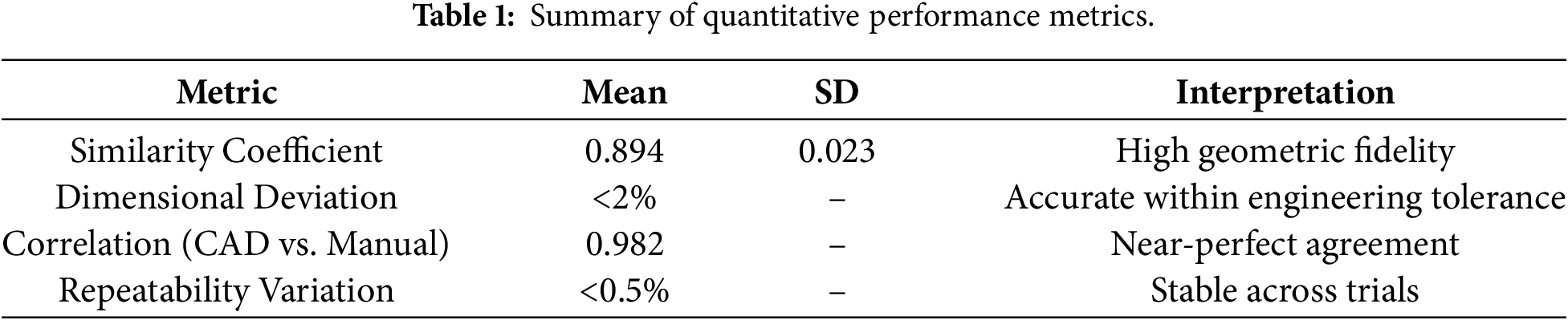
The similarity verification method, described in Section 5, was applied to evaluate multiple reconstructed PCB cases. Statistical analysis of the similarity scores across test samples revealed a mean similarity coefficient of 0.894 with a standard deviation of 0.023, indicating consistent performance across varying board geometries and component densities.
The distribution of similarity values follows a narrow Gaussian profile, as depicted in Fig. 9, signifying that deviations between reconstructed and ground-truth geometries are both minimal and randomly distributed. This consistency demonstrates that the reconstruction process maintains dimensional accuracy independent of layout complexity or lighting variation.
7.2 Correlation between CAD and Manual Measurements
To further validate dimensional accuracy, key geometric features—such as component spacing, board width, and connector alignment—were compared between the reconstructed CAD models and manually measured references obtained via vernier calipers. The correlation coefficient between the two measurement sets was found to be 0.982, confirming near-perfect linear correspondence. The average absolute dimensional deviation remained below 2%, well within acceptable tolerance for engineering documentation and mechanical integration applications.
These results suggest that the combination of telecentric optics and deep learning detection provides measurement reliability comparable to conventional manual metrology while dramatically improving throughput and reproducibility.
7.3 Repeatability and Reproducibility
The system’s repeatability was examined by reconstructing the same PCB sample five times under identical conditions. The variation in similarity score between iterations was less than 0.5%, demonstrating excellent intra-system stability. Reproducibility tests performed on different boards of similar type yielded comparable results, confirming that the framework can generalize across multiple hardware configurations without recalibration or retraining.
The combined statistical and correlation analyses confirm that the proposed method achieves a strong balance between accuracy, automation, and scalability. As summarized in Table 1, the quantitative metrics show that errors arising from component detection, image stitching, and CAD placement remain within the submillimeter range, exerting negligible influence on the global reconstructed geometry.
These results reinforce that the framework is well-suited not only for reverse engineering and digital archiving but also for precision-oriented tasks such as automated inspection, enclosure fitting, and digital twin creation. The quantitative evidence therefore establishes a solid foundation for integrating the system into next-generation smart manufacturing pipelines.
8 Conclusion and Future Perspectives
This paper has presented an automated imaging-to-CAD reconstruction framework that combines telecentric imaging, deep learning–based component detection, and CAD automation to achieve high-fidelity digital reconstruction of printed circuit boards (PCBs). The proposed system provides a coherent and unified workflow that bridges the long-standing gap between optical metrology and digital design automation, enabling raw visual data to be transformed directly into standardized, design-ready 3D CAD assemblies.
The integration of a telecentric optical system with a YOLO-based detection model ensures distortion-free imaging and reliable semantic recognition of electronic components, while the 3D model mapping strategy and Fusion 360 API enable precise and automated assembly generation in the CAD environment. Quantitative evaluation demonstrated that the framework achieves a similarity score of 0.894 and maintains dimensional deviations within 2% of manual reference measurements, confirming its geometric fidelity. Furthermore, comparative analyses indicate that the proposed approach provides an effective balance of accuracy, automation, and practical applicability when benchmarked against industrial image-analysis systems and conventional manual metrology.
Despite the promising results, this work has several limitations. The proposed framework was evaluated on a relatively limited PCB dataset acquired under controlled telecentric imaging conditions; therefore, its generalization to highly diverse PCB layouts and unconstrained industrial environments has not been fully validated. In addition, certain component attributes are inferred from predefined libraries or datasheets rather than reconstructed directly from visual data. Future work will focus on expanding the dataset, improving robustness under unconstrained imaging conditions, and extending the framework toward multilayer assemblies and full 3D geometry inference.
Collectively, these findings demonstrate that the proposed framework establishes a robust and extensible digital workflow for imaging-to-CAD reconstruction within the defined experimental scope. By integrating AI-driven perception with CAD-level interoperability, the system contributes to advancing smart manufacturing, knowledge-based engineering, and Industry 4.0 digital transformation, while offering a solid foundation for future extensions toward broader datasets, more complex assemblies, and enhanced generalization capabilities.
Acknowledgement: The authors gratefully acknowledge the support provided by the IMT Lab, Faculty of Engineering, Chulalongkorn University.
Funding Statement: This research was funded by the Ratchadaphiseksomphot Endowment Fund, Chulalongkorn University grant number: RSF-AnH-69-06-21-01.
Author Contributions: The authors confirm contribution to the paper as follows: study conception and design: Toa Saito, Kosuke Takano, Ratchatin Chancharoen; methodology development: Toa Saito, Kantawatchr Chaiprabha, Kosuke Takano; data collection and investigation: Toa Saito, Kantawatchr Chaiprabha; formal analysis and interpretation of results: Toa Saito, Kosuke Takano, Ratchatin Chancharoen; resource provision: Kosuke Takano, Ratchatin Chancharoen, Gridsada Phanomchoeng; draft manuscript preparation: Toa Saito, Kosuke Takano, Ratchatin Chancharoen, Gridsada Phanomchoeng; review and editing: Toa Saito, Kosuke Takano, Ratchatin Chancharoen, Gridsada Phanomchoeng; supervision and project administration: Kosuke Takano, Ratchatin Chancharoen; funding acquisition: Kosuke Takano, Ratchatin Chancharoen, Gridsada Phanomchoeng. All authors reviewed and approved the final version of the manuscript.
Availability of Data and Materials: Data available on request from the authors. The data that support the findings of this study are available from the corresponding author.
Ethics Approval: Not applicable.
Conflicts of Interest: The authors declare no conflicts of interest.
References
1. da Silva LRR, Pimenov DY, da Silva RB, Ercetin A, Giasin K. Review of applications of digital twins and industry 4.0 for machining. J Manuf Mater Process. 2025;9(7):211. doi:10.3390/jmmp9070211. [Google Scholar] [CrossRef]
2. Afeez A, Sanjay S, Kumar A. Application of CAD and reverse engineering methodology for development of complex assemblies. J Eng Des Technol. 2013;11(3):375–90. doi:10.1108/jedt-10-2011-0073. [Google Scholar] [CrossRef]
3. Ali Shah G, Polette A, Pernot JP, Giannini F, Monti M. User-driven computer-assisted reverse engineering of editable CAD assembly models. J Comput Inf Sci Eng. 2022;22(2):021014. doi:10.1115/1.4053150. [Google Scholar] [CrossRef]
4. Zhao Y, Deng X, Lai H. A deep learning-based method to detect components from scanned structural drawings for reconstructing 3D models. Appl Sci. 2066 2020;10(6):2066. doi:10.3390/app10062066. [Google Scholar] [CrossRef]
5. Eltaief A, Ben Amor S, Louhichi B, Alrasheedi NH, Seibi A. Automated assessment tool for 3D computer-aided design models. Appl Sci. 2024;14(11):4578. doi:10.3390/app14114578. [Google Scholar] [CrossRef]
6. Karami A, Menna F, Remondino F. Combining photogrammetry and photometric stereo to achieve precise and complete 3D reconstruction. Sensors. 2022;22(21):8172. doi:10.3390/s22218172. [Google Scholar] [PubMed] [CrossRef]
7. Lin R, Ji Y, Ding W, Wu T, Zhu Y, Jiang M. A survey on deep learning in 3D CAD reconstruction. Appl Sci. 2025;15(12):6681. doi:10.3390/app15126681. [Google Scholar] [CrossRef]
8. Attaran M, Attaran S, Celik BG. The impact of digital twins on the evolution of intelligent manufacturing and Industry 4.0. Adv Comput Intell. 2023;3(3):11. doi:10.1007/s43674-023-00058-y. [Google Scholar] [PubMed] [CrossRef]
9. Soori M, Arezoo B, Dastres R. Digital twin for smart manufacturing, a review. Sustain Manuf Serv Econ. 2023;2:100017. doi:10.1016/j.smse.2023.100017. [Google Scholar] [CrossRef]
10. Liu Z, He P, Wang F. PCB defect images super-resolution reconstruction based on improved SRGAN. Appl Sci. 2023;13(11):6786. doi:10.3390/app13116786. [Google Scholar] [CrossRef]
11. Yin X, Zhao Z, Weng L. MAS-YOLO: a lightweight detection algorithm for PCB defect detection based on improved YOLOv12. Appl Sci. 2025;15(11):6238. doi:10.3390/app15116238. [Google Scholar] [CrossRef]
12. Starodubov D, Danishvar S, Al Rahman M, Abu Ebayyeh A, Mousavi A. Advancements in PCB components recognition using WaferCaps: a data fusion and deep learning approach. Electronics. 2024;13(10):1863. doi:10.3390/electronics13101863. [Google Scholar] [CrossRef]
13. He Z, Lian Y, Wang Y, Lu Z. A comprehensive review of research on surface defect detection of PCBs based on machine vision. Results Eng. 2025;27(2):106437. doi:10.1016/j.rineng.2025.106437. [Google Scholar] [CrossRef]
14. Wang R, Duan F, Fu X, Li J. Method for measuring geometric dimensions of micro parts based on a telecentric camera. Opt Express. 2025;33(11):23580–95. doi:10.1364/OE.565038. [Google Scholar] [PubMed] [CrossRef]
15. Makhesana MA, Bagga PJ, Patel KM, Patel HD, Balu A, Khanna N. Comparative analysis of different machine vision algorithms for tool wear measurement during machining. J Intell Manuf. 2025;36(7):4567–91. doi:10.1007/s10845-024-02467-3. [Google Scholar] [CrossRef]
16. Mazher Iqba JL, Parveen MS, Arun S. Image stitching and 2D to 3D image reconstruction for abnormal activity detection. Int J Comput Appl. 2016;133(17):1–7. doi:10.5120/ijca2016908078. [Google Scholar] [CrossRef]
17. Escorcia Hernández JM, Chemori A, Aguilar Sierra H. Chapter 1—Introduction, in modeling and nonlinear robust control of delta-like parallel kinematic manipulator. In: Escorcia Hernández JM, Chemori A, Aguilar Sierra H, editors. Modeling and nonlinear robust control of delta-like parallel kinematic manipulators. Cambridge, MA, USA: Academic Press; 2023. p. 1–19. doi:10.1016/B978-0-32-396101-1.00008-X. [Google Scholar] [CrossRef]
18. Cao Y, Yao Y, Lu L. Design of a double-telecentric machine vision lens with continuously adjustable magnification and low distortion. Appl Opt. 2025;64(13):3456–64. doi:10.1364/AO.557850. [Google Scholar] [PubMed] [CrossRef]
19. Meng J, Guo L, Hao W, Jain DK. A surface defect detection method for electronic products based on improved YOLOv11. PLoS One. 2025;20(10):e0334333. doi:10.1371/journal.pone.0334333. [Google Scholar] [PubMed] [CrossRef]
20. Bergmann RB, Kalms M, Falldorf C. Optical in-process measurement: concepts for precise, fast and robust optical metrology for complex measurement situations. Appl Sci. 2021;11(22):10533. doi:10.3390/app112210533. [Google Scholar] [CrossRef]
21. Javaid M, Haleem A, Pratap Singh R, Suman R. Industrial perspectives of 3D scanning: features, roles and it’s analytical applications. Sens Int. 2021;2(1):100114. doi:10.1016/j.sintl.2021.100114. [Google Scholar] [CrossRef]
22. Hu Y, Zhang L. A telecentric-perspective heterogeneous stereo vision system and its calibration. Opt Laser Technol. 2025;192:113614. doi:10.1016/j.optlastec.2025.113614. [Google Scholar] [CrossRef]
23. Zhang L, Zhang X, Li H, Cao Y, Wang R. Calibration of an active binocular vision system with telecentric lenses for 3D micro-assembly. Measurement. 2025;247(11):116771. doi:10.1016/j.measurement.2025.116771. [Google Scholar] [CrossRef]
24. Chhetri SP, Bhat S, Timalsina P, Magar BT. Detection of missing component in PCB using YOLO. Int J Engin Technol. 2023;1(1):62–71. doi:10.3126/injet.v1i1.60902. [Google Scholar] [CrossRef]
25. Yao L, Liu H. Design and analysis of high-accuracy telecentric surface reconstruction system based on line laser. Appl Sci. 2021;11(2):488. doi:10.3390/app11020488. [Google Scholar] [CrossRef]
26. Lian D, Yang R, Guo M, Gao S, Huang J, Li J, et al. Telecentric imaging-based dimensional measurement for rotational components with magnification and edge localization error correction. IEEE Trans Instrum Meas. 2025;74:5045309–9. doi:10.1109/TIM.2025.3612595. [Google Scholar] [CrossRef]
27. Gümeli C, Dai A, Nießner M. Roca: robust cad model retrieval and alignment from a single image. In: Proceedings of the IEEE/CVF Conference on Computer Vision and Pattern Recognition 2022; 2022 Jun 18–24; New Orleans, LA, USA. [Google Scholar]
28. Nguyen VT, Kieu XT, Chu DT, HoangVan X, Tan PX, Le TN. Deep learning-enhanced defects detection for printed circuit boards. Results Eng. 2025;25(3):104067. doi:10.1016/j.rineng.2025.104067. [Google Scholar] [CrossRef]
29. Zhang K. Using deep learning to automatic inspection system of printed circuit board in manufacturing industry under the internet of things. ComSIS. 2023;20(2):723–41. doi:10.2298/csis220718020z. [Google Scholar] [CrossRef]
30. Lin HD, Wu HL, Lin CH. A deep transfer learning-based visual inspection system for assembly defects in similar types of manual tool products. Sensors. 2025;25(6):1645. doi:10.3390/s25061645. [Google Scholar] [PubMed] [CrossRef]
31. Huo X. Development of a real-time printed circuit board (PCB) visual inspection system using you only look once (YOLO) and fuzzy logic algorithms. J Intell Fuzzy Syst. 2023;45(3):4139–45. doi:10.3233/jifs-223773. [Google Scholar] [CrossRef]
32. Khan RU, Shah F, Ali Khan A, Tahir H. Advancing PCB quality control: harnessing YOLOv8 deep learning for real-time fault detection. Comput Mater Contin. 2024;81(1):345–67. doi:10.32604/cmc.2024.054439. [Google Scholar] [CrossRef]
33. Chen W, Ke X, Meng S. Small defect detection in printed circuit boards based on the multiscale edge strengthening and an improved YOLOv10. Sci Rep. 2025;15(1):36445. doi:10.1038/s41598-025-20387-x. [Google Scholar] [PubMed] [CrossRef]
34. Luo S, Wan F, Lei G, Xu L, Ye Z, Liu W, et al. EC-YOLO: improved YOLOv7 model for PCB electronic component detection. Sensors. 2024;24(13):4363. doi:10.3390/s24134363. [Google Scholar] [PubMed] [CrossRef]
35. Tang J, Liu S, Zhao D, Tang L, Zou W, Zheng B. PCB-YOLO: an improved detection algorithm of PCB surface defects based on YOLOv5. Sustainability. 2023;15(7):5963. doi:10.3390/su15075963. [Google Scholar] [CrossRef]
36. Zhou Z, Zhu Q, Luo J, Feng M, Wang Y, Jiang T, et al. A feature disentanglement method for image stitching of printed circuit boards. IEEE Trans Instrum Meas. 2025;74(11):5018113. doi:10.1109/TIM.2025.3547509. [Google Scholar] [CrossRef]
37. Yu Y, Gonzalez-Caceres A, Scheidegger S, Somanath S, Hollberg A. Deep learning-based scalable image-to-3D facade parser for generating thermal 3D building models. Autom Constr. 2025;179(1):106449. doi:10.1016/j.autcon.2025.106449. [Google Scholar] [CrossRef]
38. Pasinetti S, Nuzzi C, Luchetti A, Zanetti M, Lancini M, De Cecco M. Experimental procedure for the metrological characterization of time-of-flight cameras for human body 3D measurements. Sensors. 2023;23(1):538. doi:10.3390/s23010538. [Google Scholar] [PubMed] [CrossRef]
39. Zhang X, Wang H, Dong H. A survey of deep learning-driven 3D object detection: sensor modalities, technical architectures, and applications. Sensors. 2025;25(12):3668. doi:10.3390/s25123668. [Google Scholar] [PubMed] [CrossRef]
40. Nikouei M, Baroutian B, Nabavi S, Taraghi F, Aghaei A, Sajedi A, et al. Small object detection: a comprehensive survey on challenges, techniques and real-world applications. Intell Syst Appl. 2025;27(1):200561. doi:10.1016/j.iswa.2025.200561. [Google Scholar] [CrossRef]
41. Luo Y, Wang X, Liao Y, Fu Q, Shu C, Wu Y, et al. A review of homography estimation: advances and challenges. Electronics. 2023;12(24):4977. doi:10.3390/electronics12244977. [Google Scholar] [CrossRef]
42. Yuan Z, Shi J, Huang Y. OpenECAD: an efficient visual language model for editable 3D-CAD design. Comput Graph. 2024;124(4):104048. doi:10.1016/j.cag.2024.104048. [Google Scholar] [CrossRef]
Cite This Article
 Copyright © 2026 The Author(s). Published by Tech Science Press.
This work is licensed under a Creative Commons Attribution 4.0 International License , which permits unrestricted use, distribution, and reproduction in any medium, provided the original work is properly cited.
 Downloads
 Citation Tools