
 Submit a Paper
 Propose a Special lssue
 Open Access
ARTICLE

A Coprocessor Architecture for 80/112-bit Security Related Applications
1 Department of Computer Engineering, Umm Al-Qura University, Makkah, 21955, Saudi Arabia
* Corresponding Author: Muhammad Rashid. Email:
Computers, Materials & Continua 2023, 74(3), 6849-6865. https://doi.org/10.32604/cmc.2023.032849
Received 31 May 2022; Accepted 09 September 2022; Issue published 28 December 2022
 View Full Text
 Download PDF
Abstract
We have proposed a flexible coprocessor key-authentication architecture for 80/112-bit security-related applications over field by employing Elliptic-curve Diffie Hellman (ECDH) protocol. Towards flexibility, a serial input/output interface is used to load/produce secret, public, and shared keys sequentially. Moreover, to reduce the hardware resources and to achieve a reasonable time for cryptographic computations, we have proposed a finite field digit-serial multiplier architecture using combined shift and accumulate techniques. Furthermore, two finite-state-machine controllers are used to perform efficient control functionalities. The proposed coprocessor architecture over and is programmed using Verilog and then implemented on Xilinx Virtex-7 FPGA (field-programmable-gate-array) device. For and , the proposed flexible coprocessor use 1351 and 1789 slices, the achieved clock frequency is 250 and 235 MHz, time for one public key computation is 40.50 and 79.20 μs and time for one shared key generation is 81.00 and 158.40 μs. Similarly, the consumed power over and is 0.91 and 1.37 mW, respectively. The proposed coprocessor architecture outperforms state-of-the-art ECDH designs in terms of hardware resources.Keywords
Due to the exponential growth in technology, millions of users want to interact with the internet through IoT devices, and the requirement for this enormous connectivity raises security threats [1–3]. Therefore, several security services can be achieved either by employing symmetric or asymmetric (or public-key) cryptographic algorithms. Comparatively, the latter offers more increased security as two distinct keys are involved in cryptographic computation(s) [2]. On the other hand, a single key is needed in the case of symmetric algorithms/protocols. Moreover, each cryptographic algorithm (either related to symmetric or public-key) contains different messages and key lengths for a certain level of security achievement [4,5]. For 80-bit symmetric-key security achievement, Rivest-Shamir-Adleman (RSA) and Elliptic Curve Cryptography (ECC) require 1024-bit and 160-bit key lengths [4,5]. Similarly, for identical security to 112-bits, the RSA and ECC require 2048-bit and 224-bit key lengths. For security equivalent to AES-128, the RSA and ECC need 3072-bit and 256-bit lengths. Consequently, for a similar security level, ECC is an attractive option as it offers several additional benefits in terms of lower bandwidth, lower computational/processing efforts, lower power consumption, and lower area cost [6].
The ECC contains a four-layer model. The uppermost layer, known as the protocol layer, determines the execution of (i) encryption/decryption, (ii) signature-generation/verification, (iii) key-authentication, etc. For the computation of these operations, the most frequently used protocols are Elliptic-curve Diffie Hellman (ECDH) [7], Elliptic-curve Digital Signature Algorithm (ECDSA) [8] and Elliptic-curve Menezes Qu–Vanstone (ECMQV) [9]. The ECMQV, ECDSA and ECDH protocols are responsible to compute encryption/decryption, signature-generation/verification and key-authentication, respectively. To implement these protocols (ECDSA, ECDH and ECMQV), point multiplication (PM) is essential to execute (third layer of ECC model). Moreover, in Elliptic curves, the PM is the considerable computationally intensive operation [6,10–13]. The implementation of PM depends on the computation of layer two operations, i.e., point addition (PA), and doubling (PD). These operations (PA and PD) depend on layer one. The corresponding layer one operations are finite field (FF) addition, multiplication, squaring, inversion and reduction.
In addition to the ECC layer model, the prime, i.e.,
Over
Several applications demand higher security. One of the examples includes the fourth industrial revolution (also named industry 4.0) which brings rapid growth in technology, industries and societal patterns due to the demand for increasing interconnectivity of several devices over the unsecured internet. Moreover, industry 4.0 emphasizes the notion of automation of numerous applications to facilitate human daily life [14]. More specifically, in the case of digitalization, automation requires higher security, e.g., key authentication or key agreement. For example, for radio-frequency-identification-network (RFID) applications, key authentication is essential when scanning the bar codes on different products in shopping malls [18–22]. Automotive mobile vehicles are another application where authentication is critical to start secure communication [23]. Generally, these include intra or inter-mobile communications with several devices, e.g., vehicle-to-phone, vehicle-to-vehicle, phone-to-phone, etc. The term intra determines the wired/wireless communication inside the sensing network while inter means the communication with embedded devices outside the sensing network. We have provided intra-mobile connectivity of the several devices in Fig. 1 where the Node1, Node2 and Node3 are the wireless sensor nodes (WSN) that determine the connectivity of several embedded devices with the gateway.
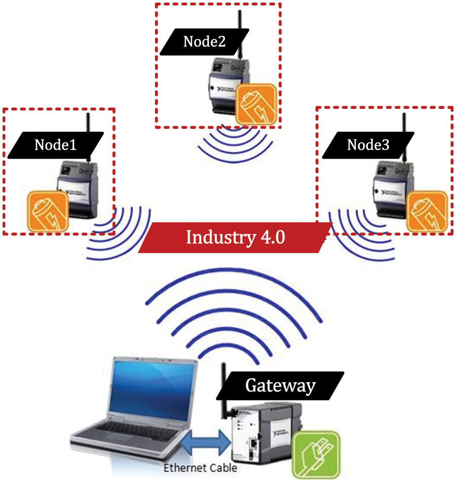
Figure 1: Intra-mobile connectivity of several devices [23]
To achieve higher security hardware-based implementations are more suitable when compared to software-based implementations. Therefore, an ECC design is described in [17] where an FPGA-based sensor node has been presented. They have targeted prime and binary fields with supported key lengths of 192 and 163. Moreover, their design is compliant with the IEEE802.15.4 standard. To reduce the hardware resources, they have reused the embedded resources of the utilized FPGA, i.e., Xilinx Artix-7.
Some ASIC and FPGA designs of ECC for RFID applications are described in [18,21]. In [18], an efficient architecture of ECC over
The ECC-based hardware accelerators specific to wireless sensor nodes on ASIC and FPGA platforms are described in [24–28]. In [24], a new ECC-based protocol followed with a coprocessor hardware design for key distribution in wireless sensor nodes is presented over
The most recent ECC published designs for securing several other cryptographic applications are described in [11,13,29,30]. In [11], a two-stage pipelined design is reported over
The hardware accelerators of ECC are specifically concentrating on the hardware resource optimizations and decreasing the power consumption for wireless sensor nodes and RFID applications [13,18,21,24–28]. A schoolbook multiplication method is frequently employed in the literature as it reduces the hardware resources and achieves lower power consumption. With minimum hardware resources and low power consumptions, the computational time (latency or throughput) is also important to exchange the cryptographic keys in a reasonable time. It is essential to provide that the performance of polynomial multiplier determines the performance of the entire ECDH protocol as it requires frequent polynomial multiplications for computation. In literature, the most commonly used Karatsuba multiplier, as employed in [13], results in higher resources and is not feasible for wireless sensor nodes and RFID applications. The schoolbook multiplication method of [21] is expensive in terms of computational time. Therefore, an optimal multiplier is needed to achieve the low-area and high-performance footprints for meeting standards for wireless sensor nodes and RFID-related applications. Consequently, to address these issues our contributions are as follows:
• Coprocessor architecture: We have proposed a key-authentication coprocessor architecture for 80/112-bit security-related applications over
• Flexibility: In our proposed coprocessor architecture, the flexibility is offered using a serial interface by placing input/output buffers to load/produce x and y coordinates of secret, public, and shared keys sequentially (bit-by-bit).
• Polynomial multiplication architecture: To reduce the hardware resources and to achieve a reasonable time for cryptographic computations, we have proposed a finite field digit-serial multiplier architecture over
• Control blocks: Finally, two finite-state-machines (FSM) are implemented to efficiently compute the public and shared keys.
The proposed coprocessor architecture is programmed using Verilog and then implemented on Xilinx Virtex-7 FPGA. Over
The rest of this article is organized as: Section 2 presents the relevant background. The proposed coprocessor architecture is presented in Section 3. The achieved results and performance comparison are discussed in Section 4. The article is concluded in Section 5.
This section describes the essential mathematical background required for the computation of operations of ECC.
Key-authentication protocol (ECDH): As discussed earlier in Section 1, the ECDH protocol (associated with the uppermost layer model of ECC) is required to perform key agreement or key-authentication between two sensor nodes. Let us make an example to describe the key agreement mechanism of the ECDH protocol. We have shown three nodes (Node1, Node2 and Node3) in Fig. 1. If Node1 wants to communicate with Node2 then the ECDH steps include: (i) Node1 and Node2 use the same ECC configurations to prompt the required setup, (ii) computation of PM at each node (Node1 and Node2) for public key generation, (iii) exchange of generated public keys between two nodes (Node1 and Node2 in this demonstration example), and (iv) computation of PM on Node1 and Node2 for shared key generation. For mathematical structures and additional descriptions of ECDH protocol, we refer readers/designers to follow [6,14].
Point multiplication over
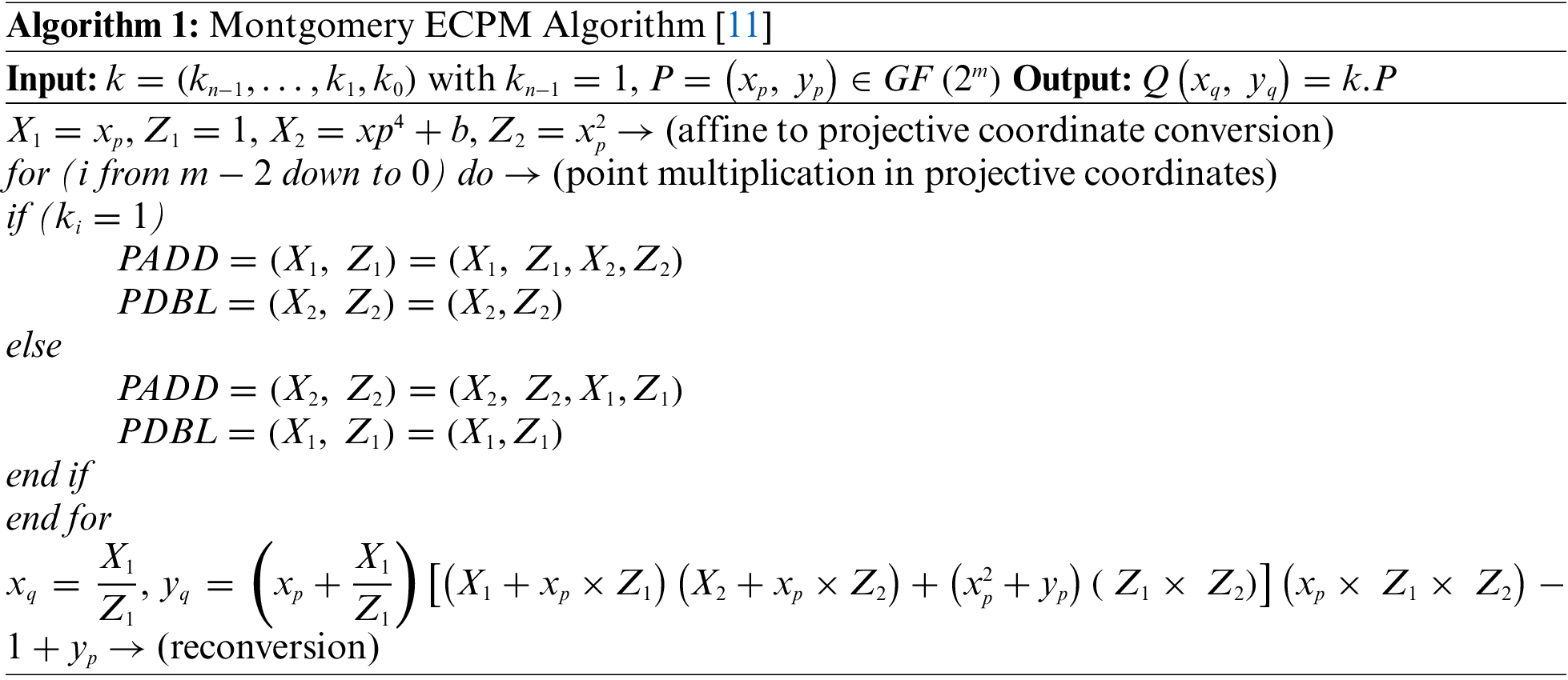
The inputs to Algorithm 1 are (i) an initial point P with x and y coordinates, i.e.,
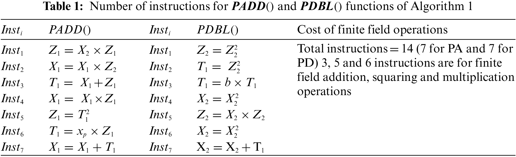
Columns one and two give the PA information in terms of sequence of instructions (i.e.,
Our proposed design is presented in Fig. 2. It contains (i) a control unit, (ii) input and output buffers and (iii) an ECC unit. The related details of these blocks are as follows.
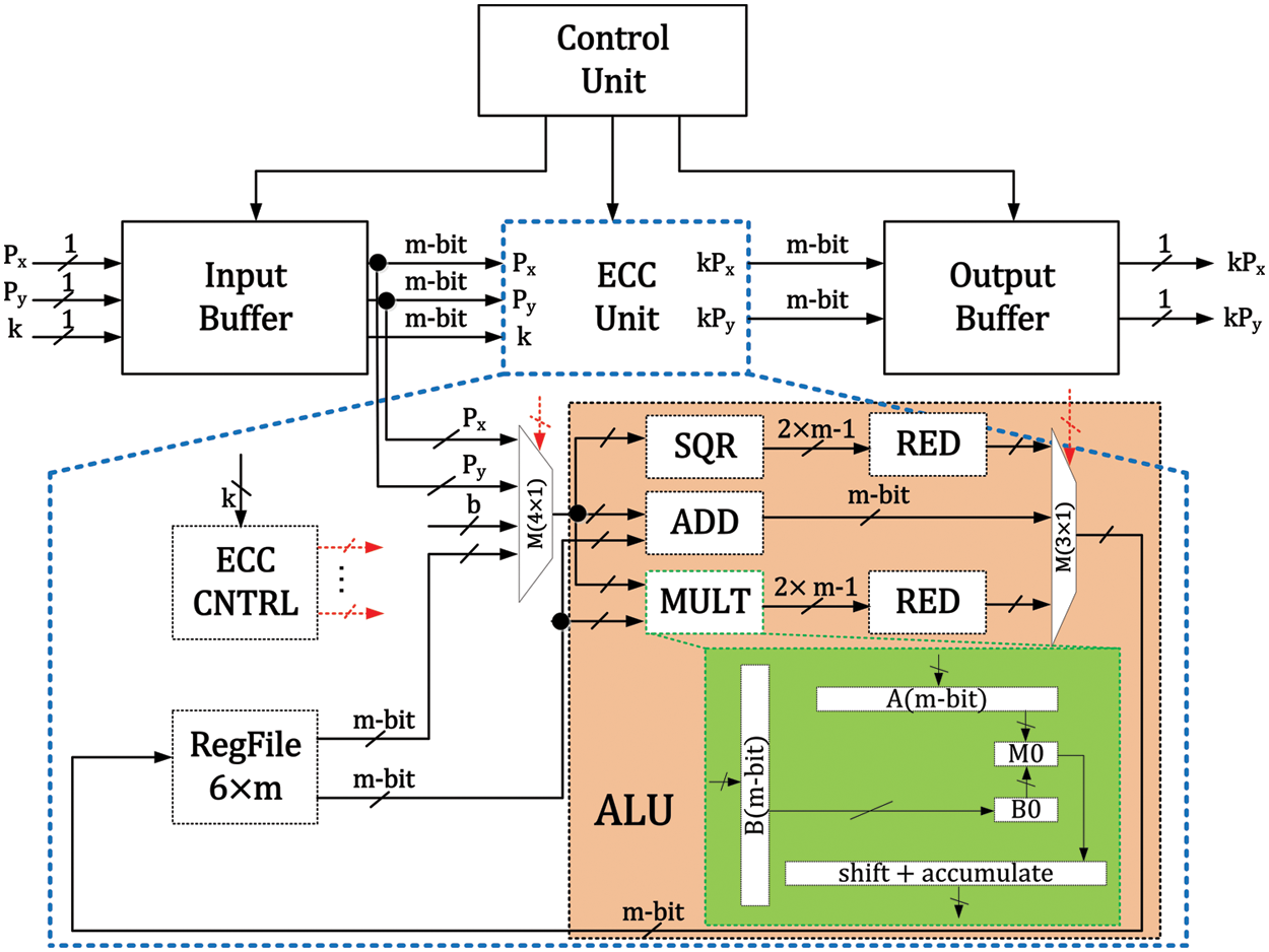
Figure 2: Proposed elliptic curve processor architecture
It generates the corresponding control signals for input/output buffers and the ECC unit. It contains three states: (i) LIP, (ii) SKG and (iii) LOP. The corresponding details of these states (LIP, SKG and LOP) are as follows.
LIP: It is responsible to load the input parameters, i.e., x and y coordinates of an input point P, and x and y coordinates of a public key of another node. The objective is the generation of a shared key for ECC unit. After loading the input parameters, it puts a
SKG: The ECDH protocol requires PM operation twice. The initial PM is for the generation of x and y coordinates of the public key. The second PM computation is required for the generation of x and y coordinates of a shared key. Therefore, the objective of an SKG state is to wait until the generation of x and y coordinates of either the public or shared keys. After generating the required public or shared keys, the control unit sets a
LOP: The purpose of the LOP states is to load the x and y coordinates of the public or shared keys on the output pins (i.e.,
The input buffer block comprises three
The ECC unit contains (i) a storage system, (ii) an arithmetic and logic unit (ALU) and (iii) a controller (ECC CNTRL), as shown in Fig. 2. Moreover, for routing purposes, a
3.3.1 Storage System (RegFile)
A
3.3.2 Arithmetic and Logic Unit (ALU)
The pink color in Fig. 2 shows the ALU that contains an adder (ADD), squarer (SQR), multiplier (MULT) and two reduction (RED) blocks (connected one after each SQR and MULT). Moreover, for routing purposes, a
The polynomial multiplication computation specifies the performance of the PM architecture [2,11,17–19,21,27,28,30–32]. For multiplying two
Proposed digit-serial multiplier architecture: Our proposed digit-serial polynomial multiplication architecture (24-bits) is shown with the green color in Fig. 2. The reason to select a 24-bits digit size is to obtain an optimal computational cost with minimum hardware resource utilization. The longer digit length reduces clock cycles requirement but utilizes more hardware resources and consumes more power which is not feasible for wireless sensor nodes and RFID applications [19,21]. With this compliance, we have employed a 24-bit digit size in our multiplication architecture of Fig. 2 where two
For the computation of one
3.3.3 Dedicated Controller (ECC CNTRL) and Clock Cycles Calculation
The
• Affine to projective coordinates conversion: Affine to projective conversions is performed from state 1 to state 6. Each state requires one clock cycle. So a total of six clock cycles are needed to compute affine to projective conversions.
• PM in projective coordinates: Columns two and four of Table 1 shows that each
• Reconversion from projective to affine coordinates: When the processor executes the
3.4 Total Clock Cycle Calculations
The total clock cycles of our proposed processor architecture over
In Eqs. (1) and (2), m shows the targeted field length (i.e., 163 and 233) and c determines the digit length of 24-bits. The additional details are given below.
• Affine to projective coordinates conversion: A numerical value of 6 before the square brackets determine the clock cycles for affine to projective conversions.
• PM in projective coordinates: In Eqs. (1) and (2),
• Reconversion from projective to affine coordinates: As shown in reconversion part of Algorithm 1, two finite field inversions are involved to execute the reconversion step. Therefore, over
To describe the implementation results, we have first provided the simulation waveform in Section 4.1.1. After that, the implementation results are reported in Section 4.1.2. Finally, the schematic waveform after the circuit place and route is shown in Section 4.1.3.
The simulation waveform over
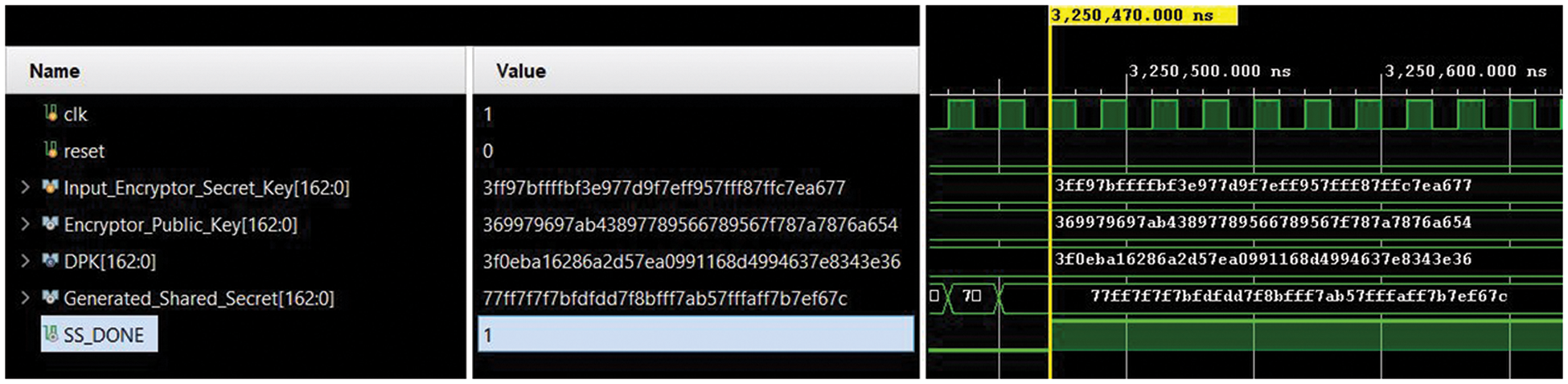
Figure 3: RTL simulation waveform (captured on Vivado 2019.2)
Our proposed coprocessor architecture over
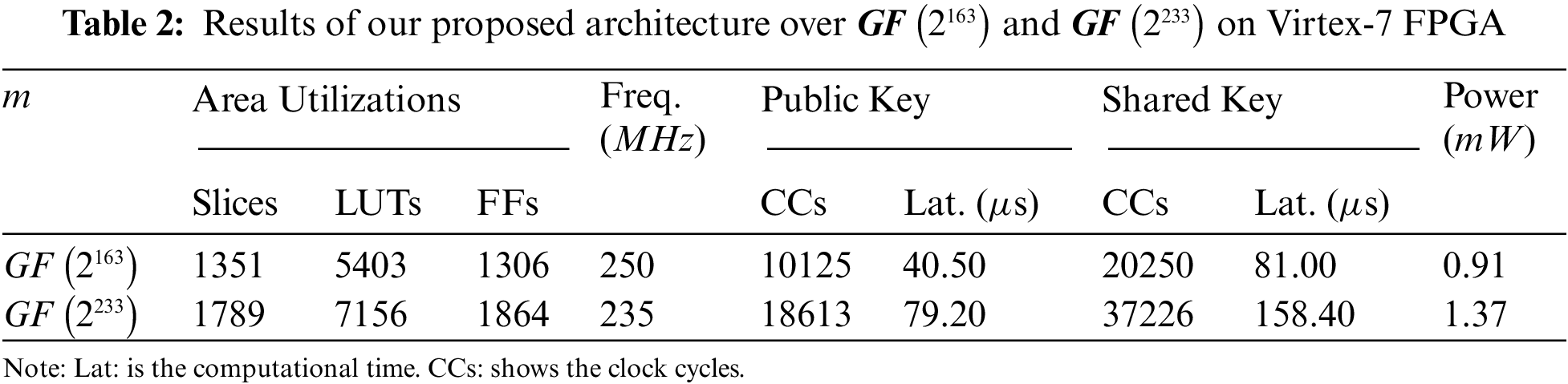
Due to different field lengths (i.e.,
Despite the hardware resources and operational frequency, our design requires 10125 and 20250 cycles for one public and shared keys computation over
Utilization of a digit-serial multiplier with a smaller digit size of 24-bit results in lower power consumption of 0.91 and 1.37 mW over
The circuit layout of our proposed coprocessor architecture over

Figure 4: Circuit layout of the proposed coprocessor architecture over
The comparison with state-of-the-art is shown in Table 3. The reference design and publication years are displayed in column one. The implemented binary field length along with cryptographic operation is given in column two. Column three presents the targeted FPGA device. The values presented before the parenthesis in column four are the FPGA slices while a value inside the parenthesis is the FPGA LUTs. The operational frequency (in
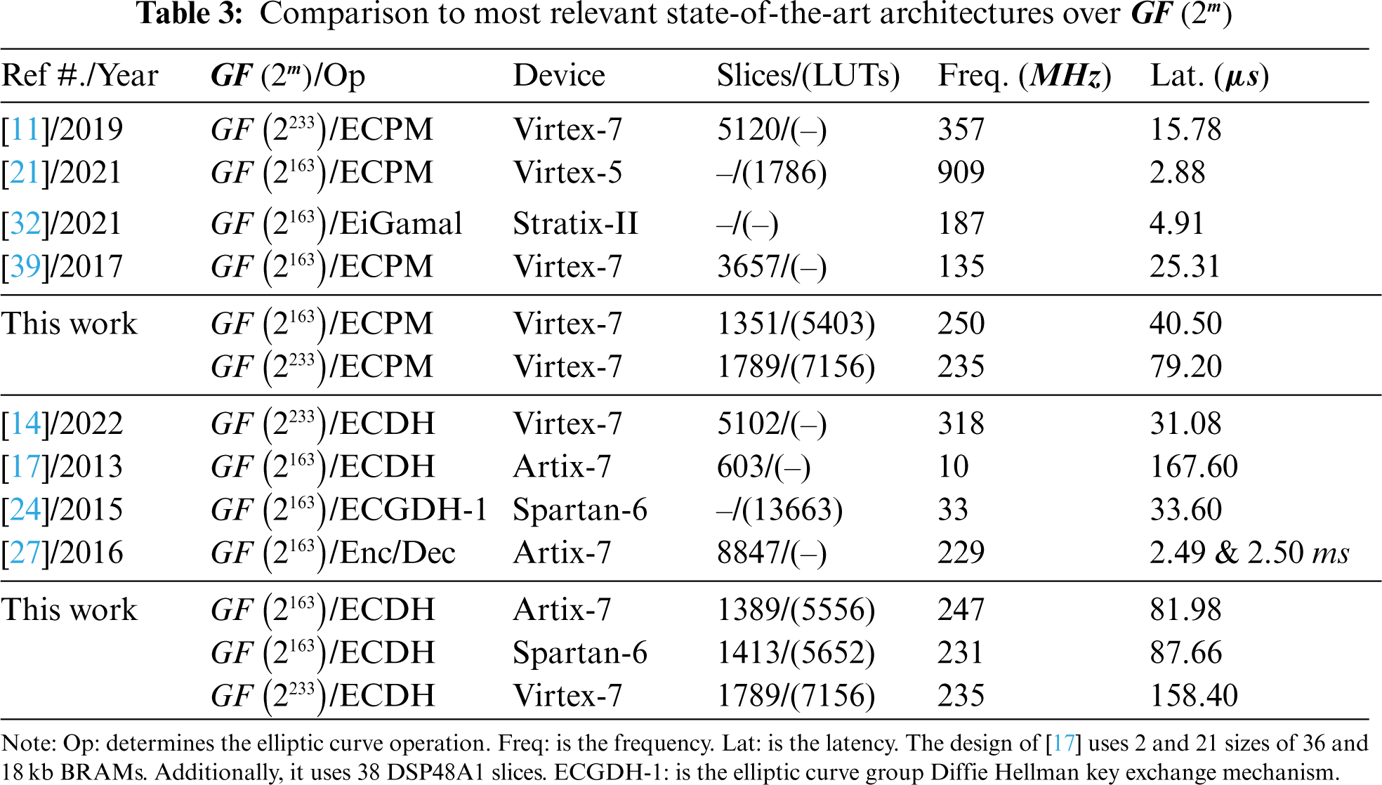
4.2.1 Comparison with ECPM Designs
On Virtex-7 over
As shown in Table 3, the architecture of [21] over
Apart from the hardware resources and timing results, the power consumption of [21] is 0.73 mW for one PM execution. In our work, a 0.91 mW is consumed for one shared key generation using ECDH protocol. Furthermore, our design utilizes Montgomery PM algorithm for the implementation of the ECDH protocol of ECC as it is inherently secure against timing and power analysis attacks. On the other hand, the Lopez Dahab PM algorithm is used in [21]. In Lopez Dahab PM algorithm, swapping between the PA and PD computations is needed whenever the inspected value of the key-bit becomes 1. The need for swapping requires additional clock cycles which shows that the architecture of [21] is not secure against the timing and power analysis attacks. To summarize, our architecture is protected against timing and power analysis attacks and consumes a comparable power than the power consumption of [21].
The Stratix-II design of [32] achieves an operational frequency of 187 MHz that is comparatively 1.33 (ratio of 250 with 187) times lower than our Virtex-7 implementation over
4.2.2 Comparison to Key-Authentication Architectures
The most recent design of [14] for key-authentication using ECDH protocol over
The efficient implementation of [17] for key authentication using ECDH protocol over
On similar Spartan-6 device, the design of [24] over
This article has proposed a flexible coprocessor key-authentication architecture for 80/112-bit security-related applications over
Funding Statement: This project has received funding by the NSTIP Strategic Technologies program under Grant Number 14-415 ELE1448-10, King Abdul Aziz City of Science and Technology of the Kingdom of Saudi Arabia.
Conflicts of Interest: The authors declare that they have no conflicts of interest to report regarding the present study.
References
1. M. Rana, Q. Mamun and R. Islam, “Lightweight cryptography in IoT networks: A survey,” Future Generation Computer Systems, vol. 129, pp. 77–89, 2022. [Google Scholar]
2. M. Rashid, M. Imran, A. R. Jafri and T. F. Al-Somani, “Flexible architectures for cryptographic algorithms: A systematic literature review,” Journal of Circuits Systems and Computers (JCSC), vol. 28, no. 3, pp. 35, 2019. [Google Scholar]
3. E. Anaya, J. Patel, P. Shah, V. Shah and Y. Cheng, “A performance study on cryptographic algorithms for IoT devices,” in Proc. of the Tenth ACM Conf. on Data and Application Security and Privacy, New York, USA, pp. 159–161, 2020. [Google Scholar]
4. A. Miri, “Advanced Security and Privacy for RFID Technologies,” Hershey, PA: IGI Global, pp. 1–342, 2013. [Online]. Available: https://www.igi-global.com/gateway/book/72161. [Google Scholar]
5. M. Imran and F. Shehzad, “FPGA based crypto processor for elliptic curve point multiplication (ECPM) over
6. D. Hankerson, A. J. Menezes and S. Vanstone, “Guide to Elliptic Curve Cryptography,” Henderson, NV, USA: Springer, pp. 1–311, 2004. [Online]. Available: https://link.springer.com/book/10.1007/b97644. [Google Scholar]
7. R. Housley, “Use of the Elliptic Curve Diffie-Hellman Key Agreement Algorithm with x25519 and x448 in the Cryptographic Message Syntax (CMS),” RFC 8418, pp. 1–18, 2018. [Online]. Available: https://www.rfc-editor.org/info/rfc8418. [Google Scholar]
8. T. Pornin, “Deterministic Usage of the Digital Signature Algorithm (DSA) and Elliptic Curve Digital Signature Algorithm (ECDSA),” RFC 6979, pp. 1–79, 2013. [Online]. Available: https://www.rfc-editor.org/info/rfc6979. [Google Scholar]
9. S. Turner, D. Brown, K. Yiu, R. Housley and T. Polk, “Elliptic Curve Cryptography Subject Public Key Information,” RFC 5480, pp. 1–20, 2009. [Online]. Available: https://www.rfc-editor.org/info/rfc5480. [Google Scholar]
10. N. Pirotte, J. Vliegen, L. Batina and N. Mentens, “Design of a fully balanced ASIC coprocessor implementing complete addition formulas on weierstrass elliptic curves,” in 21st Euromicro Conf. on Digital System Design (DSD), Prague, Czech Republic, pp. 545–552, 2018. [Google Scholar]
11. M. Imran, M. Rashid, A. R. Jafri and M. Kashif, “Throughput/area optimised pipelined architecture for elliptic curve crypto processor,” IET Computers & Digital Techniques, vol. 13, no. 5, pp. 361–368, 2019. [Google Scholar]
12. B. Rashidi, “Low-cost and fast hardware implementations of point multiplication on binary edwards curves,” in Electrical Engineering (ICEEIranian Conf. on, Mashhad, Iran, pp. 17–22, 2018. [Google Scholar]
13. M. Imran, M. Rashid and I. Shafi, “Lopez dahab based elliptic crypto processor (ECP) over
14. M. Rashid, H. Kumar, S. Z. Khan, I. Bahkali, A. Alhomoud et al., “Throughput/area optimized architecture for elliptic-curve diffie-hellman protocol,” Applied Sciences, vol. 12, no. 8, pp. 1–18, 2022. [Google Scholar]
15. J. Vliegen, N. Mentens, J. Genoe, A. Braeken, S. Kubera et al., “A compact FPGA-based architecture for elliptic curve cryptography over prime fields,” in 21st IEEE Int. Conf. on Application-Specific Systems, Architectures and Processors, Rennes, France, pp. 313–316, 2010. [Google Scholar]
16. NIST. “Recommended Elliptic Curves for Federal Government Use,” FIPS PUB 1862–2: USA, pp. 1–70, 1999. [Online]. Available: https://csrc.nist.gov/csrc/media/publications/fips/186/2/archive/2000-01-27/documents/fips186-2.pdf. [Google Scholar]
17. A. De la Piedra, A. Braeken and A. Touhafi, “Extending the IEEE 802.15.4 security suite with a compact implementation of the NIST P-192/B-163 elliptic curves,” Sensors, vol. 13, no. 8, pp. 9704–9728, 2013. [Google Scholar]
18. Z. Liu, D. Liu, X. Zou, H. Lin and J. Cheng, “Design of an elliptic curve cryptography processor for RFID tag chips,” Sensors, vol. 14, no. 10, pp. 17883–17904, 2014. [Google Scholar]
19. S. Khan, W. K. Lee and S. O. Hwang, “A flexible gimli hardware implementation in FPGA and its application to RFID authentication protocols,” IEEE Access, vol. 9, pp. 105327–105340, 2021. [Google Scholar]
20. A. S. R. Oliveira, N. B. Carvalho, J. Santos, A. Boaventura, R. F. Cordeiro et al., “All-digital RFID readers: An RFID reader implemented on an FPGA chip and/or embedded processor,” IEEE Microwave Magazine, vol. 22, no. 3, pp. 18–24, 2021. [Google Scholar]
21. M. Rashid, S. S. Jamal, S. Z. Khan, A. R. Alharbi, A. Aljaedi et al., “Elliptic-curve crypto processor for RFID applications,” Applied Sciences, vol. 11, no. 15, pp. 1–16, 2021. [Google Scholar]
22. T. D. P. Bai, K. M. Raj and S. A. Rabara, “Elliptic curve cryptography based security framework for internet of things (IoT) enabled smart card,” in 2017 World Congress on Computing and Communication Technologies (WCCCT), Tiruchirappalli, India, pp. 43–46, 2017. [Google Scholar]
23. C. Ankita, “Wireless Sensor Networks,” electroSome, 2013. [Online]. Available: https://electrosome.com/wireless-sensor-networks/#google_vignette. [Google Scholar]
24. L. Parrilla, D. P. Morales, J. A. López-Villanueva, J. A. López-Ramos and J. A. Álvarez-Bermejo, “Hardware implementation of a new ECC key distribution protocol for securing wireless sensor networks,” in 2015 Conf. on Design of Circuits and Integrated Systems (DCIS), Estoril, Portugal, pp. 1–6, 2015. [Google Scholar]
25. S. Peter, O. Stecklina, J. Portilla, E. de la Torre, P. Langendoerfer et al., “Reconfiguring crypto hardware accelerators on wireless sensor nodes,” in 6th IEEE Annual Communications Society Conf. on Sensor, Mesh and Ad Hoc Communications and Networks Workshops, Rome, Italy, pp. 1–3, 2009. [Google Scholar]
26. P. Jilna, P. P. Deepthi and U. K. Jayaraj, “Optimized hardware design and implementation of EC based key management scheme for WSN,” in 10th Int. Conf. for Internet Technology and Secured Transactions (ICITST), London, UK, pp. 164–169, 2015. [Google Scholar]
27. G. Leelavathi, K. Shaila and K. R. Venugopal, “Elliptic curve cryptography implementation on FPGA using montgomery multiplication for equal key and data size over
28. M. Das and Z. Wang, “ED25519: A new secure compatible elliptic curve for mobile wireless networks security,” Jordanian Journal of Computers and Information Technology (JJCIT), vol. 8, no. 1, pp. 57–71, 2022. [Google Scholar]
29. U. Gulen and S. Baktir, “Elliptic curve cryptography for wireless sensor networks using the number theoretic transform,” Sensors, vol. 20, no. 5, pp. 1–16, 2020. [Google Scholar]
30. S. C. Seo and H. Seo, “Highly efficient implementation of NIST-compliant koblitz curve for 8-bit AVR-based sensor nodes,” IEEE Access, vol. 6, pp. 67637–67652, 2018. [Google Scholar]
31. Z. Razali, N. Muslim, S. Kahar, F. Yunos and K. Mohamed, “Improved point 5P formula for twisted edwards curve in projective coordinate over prime field,” in Int. Conf. on Decision Aid Sciences and Applications (DASA), Chiangrai, Thailand, pp. 498–502, 2022. [Google Scholar]
32. R. Amiri and O. Elkeelany, “FPGA design of elliptic curve cryptosystem (ECC) for isomorphic transformation and EC ElGamal encryption,” IEEE Embedded Systems Letters, vol. 13, no. 2, pp. 65–68, 2021. [Google Scholar]
33. S. Devi, R. Mahajan and D. Bagai, “A low complexity bit parallel polynomial basis systolic multiplier for general irreducible polynomials and trinomials,” Microelectronics Journal, vol. 115, pp. 105163, 2021. [Google Scholar]
34. S. Devi, R. Mahajan and D. Bagai, “Low complexity design of bit parallel polynomial basis systolic multiplier using irreducible polynomials,” Egyptian Informatics Journal, vol. 23, no. 1, pp. 105–112, 2022. [Google Scholar]
35. S. E. Mathe and L. Boppana, “Bit-parallel systolic multiplier over
36. M. Thirumoorthi, M. Heidarpur, M. Mirhassani and M. Khalid, “An optimized m-term karatsuba-like binary polynomial multiplier for finite field arithmetic,” IEEE Transactions on Very Large Scale Integration (VLSI) Systems, vol. 30, no. 5, pp. 603–614, 2022. [Google Scholar]
37. H. Kumar, M. Rashid, A. Alhomoud, S. Z. Khan, I. Bahkali et al., “A scalable digit-parallel polynomial multiplier architecture for NIST-standardized binary elliptic curves,” Applied Sciences, vol. 12, no. 9, pp. 1–18, 2022. [Google Scholar]
38. T. Itoh and S. Tsujii, “A fast algorithm for computing multiplicative inverses in
39. M. Imran, I. Shafi, A. R. Jafri and M. Rashid, “Hardware design and implementation of ECC based crypto processor for low-area-applications on FPGA,” in Int. Conf. on Open Source Systems & Technologies (ICOSST), Lahore, Pakistan, pp. 54–59, 2017. [Google Scholar]
40. Xilinx, “Power Analysis and Optimization,” AMD Xilinx, UG907: USA, pp. 1–112. 2016. [Online]. Available: https://docs.xilinx.com/v/u/2016.2-English/ug907-vivado-power-analysis-optimization. [Google Scholar]
41. M. Imran, Z. U. Abideen and S. Pagliarini, “An open-source library of large integer polynomial multipliers,” in 24th Int. Symp. on Design and Diagnostics of Electronic Circuits & Systems (DDECS), Vienna, Austria, pp. 145–150, 2021. [Google Scholar]
Cite This Article
 Copyright © 2023 The Author(s). Published by Tech Science Press.
This work is licensed under a Creative Commons Attribution 4.0 International License , which permits unrestricted use, distribution, and reproduction in any medium, provided the original work is properly cited.
 Downloads
 Citation Tools