
 Submit a Paper
 Propose a Special lssue
 Open Access
ARTICLE

Optical Neural Networks: Analysis and Prospects for 5G Applications
1 Department of Computer Sciences, College of Computer and Information Sciences, Princess Nourah Bint Abdulrahman University, P. O. Box 84428, Riyadh, 11671, Saudi Arabia
2 School of Information and Finance, Xuancheng Vocational & Technical College, Xuancheng, 242000, China
3 Department of Electrical Engineering, University of Engineering and Technology, P. O. Box 814, Peshawar, Pakistan
4 Islamic University Centre for Scientific Research, The Islamic University, Najaf, Iraq
5 Department of Computer Science, Independent University, Dhaka, 1208, Bangladesh
* Corresponding Author: Amel Ali Alhussan. Email:
(This article belongs to the Special Issue: Optimization for Artificial Intelligence Application)
Computers, Materials & Continua 2023, 77(3), 3723-3740. https://doi.org/10.32604/cmc.2023.039956
Received 26 February 2023; Accepted 01 July 2023; Issue published 26 December 2023
 View Full Text
 Download PDF
Abstract
With the capacities of self-learning, acquainted capacities, high-speed looking for ideal arrangements, solid nonlinear fitting, and mapping self-assertively complex nonlinear relations, neural systems have made incredible advances and accomplished broad application over the final half-century. As one of the foremost conspicuous methods for fake insights, neural systems are growing toward high computational speed and moo control utilization. Due to the inborn impediments of electronic gadgets, it may be troublesome for electronic-implemented neural systems to make the strides these two exhibitions encourage. Optical neural systems can combine optoelectronic procedures and neural organization models to provide ways to break the bottleneck. This paper outlines optical neural networks of feedforward repetitive and spiking models to give a clearer picture of history, wildernesses, and future optical neural systems. The framework demonstrates neural systems in optic communication with the serial and parallel setup. The graphene-based laser structure for fiber optic communication is discussed. The comparison of different balance plans for photonic neural systems is made within the setting of hereditary calculation and molecule swarm optimization. In expansion, the execution comparison of routine photonic neural, time-domain with and without extending commotion is additionally expounded. The challenges and future patterns of optical neural systems on the growing scale and applications of in situ preparing nonlinear computing will hence be uncovered.Keywords
Artificial intelligence (AI) is one of the foremost dynamic subjects in computer science nowadays, with basic applications in an assortment of areas such as machine vision [1,2], independent driving [3,4], and target following [5,6]. Artificial neural network (ANN), as one of the foremost critical models of fake insights, is broadly utilized in different scenarios since of its great generalization capacity and strength. The fake neural organize creates the association structure between the neurons in each layer of the neural organize and sets up the association between the neurons in each layer of the neural organize by imitating the structure of the apprehensive framework. A Integrated Circuit (IC) chip is the equipment carrier for preparing and testing today’s standard neural organize models, and conventional neural systems can run on CPUs, GPUs, Field programmable gate array (FPGA), Application specific integrated circuit (ASIC). Notwithstanding anything, the IC chip is chosen as the carrier, and the von Neumann structure will part the program and information spaces, coming about in an impressive sum of tidal information stack between the memory and the computing unit [6]. Frequent reading and writing of tidal data reduces the calculation speed and increases the energy consumption of a single calculation. Researchers mainly use two schemes of integrated enhancement and in-memory computing [6] to improve computational efficiency. But they also face challenges: On the one hand, it is unsustainable to continuously reduce the size of the transistor to improve the computation speed, and the gradual reduction of the transistor size will lead to significant quantum effects, making it difficult to improve the efficiency of the transistor [7]. On the other hand, the in-memory computing solution will face the problem of large-scale transformation of the current neural network architecture, thereby reducing the portability and compatibility of the neural network algorithms. adaptation to in-memory computing [6]. Some researchers have also used frequency domain computation schemes [8] to improve computational efficiency but also failed to eliminate problems caused by reading and writing tidal data.
In addition, higher and higher computing speeds and larger and larger neural network scales put higher requirements on the frequency response of integrated circuits, thus increasing the difficulty of chip manufacturing.
Photons are used as the basic carrier for information transmission and processing in optical (electronic) technologies. Optical (electronic) electronic technology has been employed in communication [9,10], imaging [11], radar [12], and signal processing because of its benefits of huge bandwidth, low loss, and high transfer of information compared to traditional electronic technology. Combining this technology with traditional neural network models can give full play to the unique advantages of optical (electronic) technology and is expected to break through the technical bottlenecks such as long delay and high power consumption of traditional electrical neural networks. First of all, the photonic neural network adopts the structure of storage and computing, which avoids the tidal data reading and writing problem existing in the electrical neural network, so that it can effectively reduce the computing delay while improving the computing speed [13]. Secondly, the link loss of the photonic neural network connection is low, which can effectively improve power efficiency. Compared with traditional electrical devices, optical devices have larger bandwidths and shorter response times, so they are more suitable for high-speed real-time computing of neural networks [14]. In addition, for automatic driving, image processing, and other front-end applications of optical sensing, the photonic neural network can directly process information at the physical layer, thereby avoiding the delay, power consumption, and signal-to-noise ratio degradation introduced by photoelectric conversion.
In [15], the authors described a thorough overview of the dynamical studies of multidimensional Fractional order neural network (FONNs) in continuous and discontinuous time, including Hopfield NNs (HNNs), Cohen-Grossberg NNs, and bidirectional associative memory NNs. Comparable models are also taken into consideration in real, complex, quaternion, and octonion fields. In [16], the major goal is to use a distributed event-triggered impulsive control system to synchronize several inertial signed neural networks with different time delays, with connections between neighboring nodes of the neural networks being either positive or negative. Reference [17] examined a fractional-order octonion-valued neuralnetwork’s hopf bifurcation with time delays. All of the parameters in this model would be part of the normed division algebra of octonions. The fractional-order octonion-valued neural networks may be divided into four-dimensional real-valued neural networks due to the octonion’s non-commutativity.
At present, the research of photonic neural network technology includes three typical structures: feedforward neural networks, recurrent neural networks (reservoir calculation), and spiking neural networks. At the same time, the photonic neural network is also developing in the direction of real-time training, large-scale, and application fields. This article reviews the development of photonic neural networks, expound on the staged progress made so far, and reveal future development trends and challenges.
2 Research Status of Optical Neural Networks
2.1 Feedforward Neural Network
The main feature of the feedforward neural network is that the information between the layers of the network is transmitted in one-direction from the input layer to the output layer. The network generally includes two types of structures, the fully connected neural network, and the convolutional neural network. The matrix operation in the sub-feedforward neural network relies on the triangular decomposition algorithm [18]. The triangular decomposition algorithm deploys the unity of the transmission matrix of passive and lossless devices, and it indicates that the triangular network built by the beam splitter and the phase shifter can realize unitary matrices with arbitrary parameters and scales. In 2016, the authors in [19] used a decomposition algorithm to design an integrated chip based on the Mach-Zehnder interferometer (MZI) realize any 4 × 4 unitary matrices. In the same year, the authors in [20] carried out the optimization design based on the scheme of [18] and proposed a rectangular decomposition scheme. Combined with the singular value decomposition theory, that is, any matrix is demposed into the product of two unitary matrices and a diagonal matrix, and the Mach-Zehnder interferometer (unitary matrix) and variable attenuator (diagonal matrix) can realize any matrix. In 2017, reference [21] successfully developed the world’s first computing unit chip based on the above ideas. They first used the chip to realize linear operation and then combined the nonlinear activation function of the electrical domain simulation to construct a fully connected neural network.
Fig. 1a shows the schematic diagram of the integrated optical interference unit (OIU). The number of input and output ports on the chip is four. The red structure inside the chip learn the unitary matrix, and the blue realizes the pairing. Using the chip twice can realize the linear operation of a layer of a fully connected neural network. The nonlinear operations is performed in the fully connected neural network by computer simulation of the transmission characteristics curve of the saturable absorber. They used the integrated photon interference computing unit to build a fully connected neural network model with a single hidden layer and realize the classification of four vowels. When used, the vowel signals to be recognized are modulated on the optical pulse and determine the intermediate result through the chip (the product of modulation signal with the unitary matrix and the diagonal matrix). The intermediate result is converted into an electrical signal, modulated on the optical pulse, and passed through the chip again to perform linear operation. The nonlinear activation function of computer simulation obtains the output. The fully connected network operation undergo by repeating the above procedure. The accuracy rate of vowel recognition can reach 76.7%, and the recognized confusion matrix illustrated in Fig. 1b.

Figure 1: Optical neural network illustration. (a) Interference block, (b) recognition matrices
According to [21], the photon-fully connected neural network built by the photon interference computing unit has the following advantages: 1) The chip uses optical (electronic) technology to directly map the weight matrix of each layer to the MZI phase, thereby avoiding the tidal data load problem faced by traditional electrical neural networks; 2) In the future, with the help of phase change materials (PCM), the computing speed of the chip is only limited by the chip size, the spectral width of the dispersion module, and the performance of the photodetector (PD), which makes the chip more suitable for high-speed and low-power applications. Neural network operations; 3) The computing delay of the chip will be significantly lower than that of the traditional electrical neural network.
In order to create a more complicated convolutional neural network structure, reference [22] suggested utilizing the device to calculate image convolution segmentally via time division multiplexing in 2018. A model for a convolutional neural network is established to recognize colored numerals. The delay line structure at the input end of the integrated photon interference calculation unit illustrated in Fig. 2a. The multiplication and accumulation computation of the convolution kernels at various points and the accompanying feature maps are accomplished by including a delay line structure in front of the chip’s input port. First, the input image cut into three stacked slices according to RGB and divided into blocks according to the size of the convolution kernel. Then, each segmented sub-image combined with the convolution kernel of the same size. They are elongated together into a vector and input into the optical interference chip. Next, inject the encoded vector into the configured optical interference module to realize the convolution operation. Finally, the result is subject to nonlinear processing, and after processing, a pixel in the output pattern is obtained. Repeating the above can get a layer of convolutional neural network output. The time division multiplexing method used in this work can realize image convolution, and the simple, fully connected neural network that can only perform quaternion classification to the convolutional neural network that can recognize the color image. The advantages of low power consumption and high computing speed results in improved complexity.

Figure 2: Optical CNN architecture. (a) Delay line, (b) chart for logic and timing
2.2 Storage and Pool Computing in Recurrent Neural Network
Different from the feedforward neural network, the information between the layers of the recurrent neural network (RNN) (also known as storage pool computing) not only transmits one way but also has connections between nodes and backward feedback connections [23–25]. As shown in Fig. 3a, the recurrent neural network is composed of an input layer, an intermediate layer (also known as a storage pool), and an output layer. In addition to the feedforward connections Win and Wout between the layers, there is also a storage pool. During training, only training Wout can make the entire network achieve the corresponding function. The first is to employ the parallel structure seen in Fig. 3a, in which each recurrent neural network node is comprised of an optoelectronic device. The advantage of this scheme is that it is more intuitive, and thanks to parallel computing, the calculation speed is faster. In 2011, reference [26] used the gain saturation effect and dynamic relaxation characteristics of the semiconductor optical amplifier (SOA) to construct the nonlinear connection and feedback of the recurrent neural network storage pool, respectively. In 2016, reference [27] also used a parallel structure for the recurrent neural network built using spatial optics. However, the parallel system has problems such as poor robustness, difficult scale expansion, and high cost. To solve this problem, the second scheme, namely the serial structure shown in Fig. 3b, is proposed. In this structure, many original nodes in the storage pool are implemented by a single nonlinear node in a delayed manner.

Figure 3: RNN architecture. (a) Parallel, (b) serial
In 2012, reference [28] took the lead in realizing an optoelectronic hybrid serial RNN using an optoelectronic hybrid system, as shown in Fig. 4a. The middle storage cell consists of a variable optical attenuator, delay loop, feedback photodiode, mixer, amplifier, and a Mach-Zehnder modulator. The photodiode turns the system’s output into an electrical signal, which it then reads. The system can distinguish between square and sine waves by training and adjusting the output weights. As shown in Fig. 4b, the quantized sine waves and square waves are serially input into the system and processed by the RNN, the system will serially output the classification results shown in the lower part of Fig. 4b, where 0 represents a sine wave signal, and 1 denote a square wave signal. In addition, the system can also realize functions such as nonlinear channel equalization and digital speech recognition.
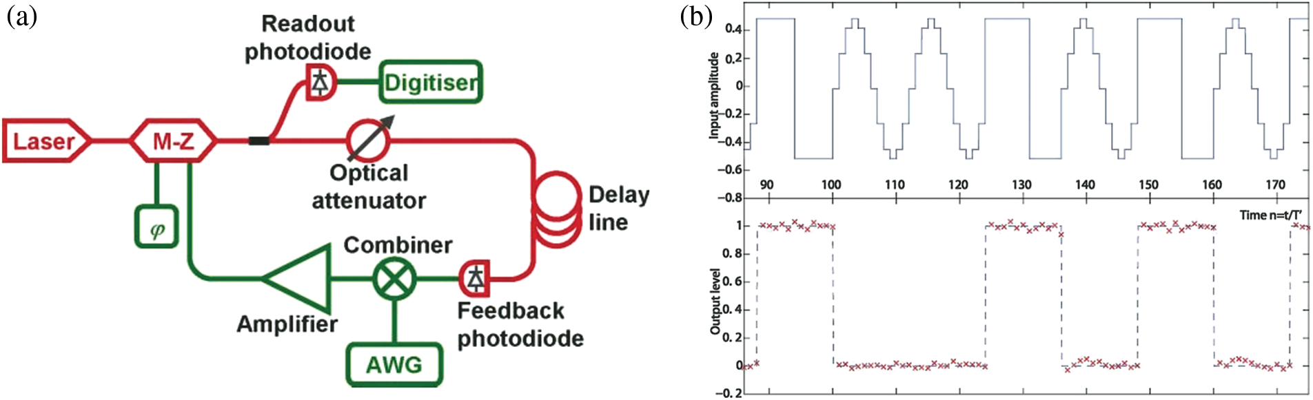
Figure 4: Optoelectronic RNN. (a) Architecture, (b) classification signals
In the same year, reference [29] utilized super-luminescent light-emitting diodes, modulators, arbitrary waveform generators, optical bandpass filters, optically tunable attenuators, beam splitters, isolators, semiconductor optical amplifiers, delay lines, photodiodes. In recent years, some progress has made in achieving the delay function in the serial neural network based on micro-ring, multi-mode interference, and other devices, in addition to directly employing the delay line to acquire the delay function [30]. The RNNs also try to use multi-level or more complex time-division multiplexing to improve the operation speed.
Spiking neural networks (SNNs) are also known as the third generation of artificial neural networks (ANNs) [31]. The simulated neurons of the SNN are closer to the biological neuron model than the feedforward neural network and the RNN. Furthermore, in every iteration of propagation, the neurons in the spiking neural network are inactive. It is triggered when its membrane potential exceeds a certain threshold. When a neuron is activated, it transmits a signal to other neurons, which causes the membrane potential of the neurons in its cascade to rise or fall. The current activation level of a neuron in a spiking neural network treated as some form of a differential equation, and its current activation level will spike following the arrival of a stimulus pulse, continue for a length of time, and then gradually fall. Spiking neural networks help in spatiotemporal data processing. The neurons in a spiking neural network structure are only connected to nearby neurons and process the input blocks separately, which improves spatial information processing capacities. However, because the training work on pulse time interval information, the information lost in the binary encoding may be re-acquired in the time information of the pulse, boosting the processing capabilities of the time information. Spiking neurons are more powerful computer units than conventional artificial neurons, has vital role in the future. Because of difficulties with the spiking neural network’s training process and hardware implementation, is not been deployed, and most spiking neural network research focus on theoretical study and fundamental structure verification. On the other hand, many researchers are presently concentrating on spiking neural network training approaches and hardware (optical) implementations.
In reference [32], a pulse processing system based on an activated graphene fiber laser was proposed, as shown in Fig. 5. The device consists principally of erbium-doped fiber (gain portion) and a graphene saturable absorber (loss part), with a pump source of 980 nm and a 1480 nm laser transmitting a pulsed stimulation signal to excite the system and create leaky integrate-and-fire (LIF-like) pulsed nerve responses.
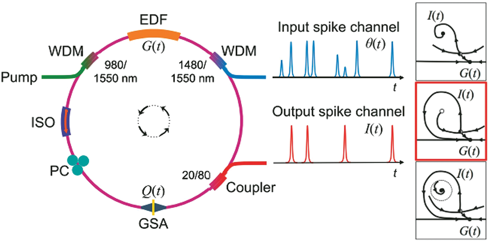
Figure 5: Structure of fiber laser based on graphene
Reference [33] proposed a neuromorphic photonic integrated circuit based on a distributed feedback (DFB) laser topology. The integrated photonic neuron shown in Fig. 6a, the response of each DFB unit to the stimulus shown in Fig. 6b.
Figure 6: DFB architecture. (a) Neural circuit, (b) response signals
The research team also considered other options for developing programmable and cascadable photonic neural networks, such as cascading research, a broadcast-and-weight network prototype [34], and a coherent optical system. This network prototype is one of them, as it is a network design presented by researchers that may allow the parallel connectivity of large-scale photonic spiking neurons.
The supervised learning method train the spiked neural networks. 1) The SpikeProp [35] algorithm, which is based on gradient descent and is suitable for multi-layer feedforward spiking neural networks; 2) The Tempotron algorithm [36], which adjusts the weights based on the difference between the output pulse sequence and the expected sequence output by neurons in the output layer. The training step determine the actual output neuron membrane potential change to match the predicted value. However, the neurons in this method do not have that capability; 3) Learning algorithms based on spike-timing-dependent plasticity (STDP), such as the Hebbian learning algorithm [37]; 4) Algorithms for remote supervised learning, such as the ReSuMe algorithm [38]; 5) The supervised learning architecture and network (SPAN) algorithm, for example, supervised learning technique based on pulse sequence convolution [39] and the power spectral density (PSD) algorithm [40].
As the intersection of artificial intelligence and optical (electronic) technology, ONN combine both benefits. Whether a feedforward neural network, a recurrent neural network, or a spiking neural network, optoelectronic devices can improve computing speed and reduce power consumption to a certain extent. Photonic neural networks still have problems as real-time training, difficulty in realizing nonlinear operations, and limited neural network scale and application. These problems not only severely restrict the development of photonic neural networks, but also limit their industrialization.
3.1 Real-Time Training Algorithm
The training problem of photonic neural networks, especially the feedforward network, is the limiting factor for expanding the application of photonic neural networks. Since photons cannot stored like electrons, the state of photons cannot directly stored; so, the back-propagation algorithm widely used in the training of electrical neural networks is difficult to transplant the training of photonic neural networks. A solution to this issue was initially put up by reference [41] in 2018, and the algorithm flow is depicted in Fig. 7. The optical field distribution and phase distribution of the phase shifter can store and gradient value can be obtained. The phase configuration in the following iteration can then be calculated, allowing the chip’s overall performance to gradually converge to a better result. It trained a neural network with two optical interference computing units (OIUs) on-chip to implement exclusive OR (XOR) logic using simulation to verify the effectiveness of the algorithm.

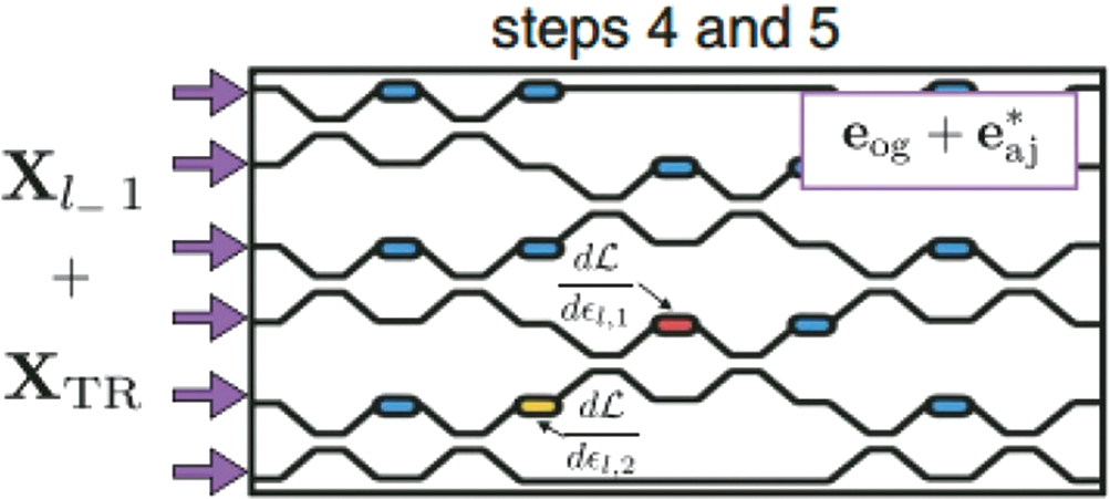
Figure 7: PNN training scheme of in situ
In the future, the algorithm can be further extended and transplanted into a larger-scale photonic neural network chip, and the chip can gradually converge to the optimal configuration through on-chip training, to complete specific functions.
At present, the training methods of photonic neural networks (PNNs) are mainly the back-propagation (BP) algorithm and stochastic gradient descent (SGD) algorithm. However, BP and SGD training strategies are difficult to implement on integrated optical chips, so most photonic neural networks need to be pre-trained by digital computers to obtain weights. Due to the restricted precision of the model representation, this training technique is not only inefficient, but it also loses its benefits in terms of speed and power consumption.
To learn hyperparameters in photonic neural networks and train them, reference [42] developed an effective training technique based on a neuroevolution approach employing genetic algorithms (GA) and particle swarm optimization (PSO). For performance evaluation, the trained photonic neural network is employed to complete the classification job, and the calculations reveal that its accuracy and stability are sufficient to compete with classical learning techniques. To verify the effectiveness of the algorithm, reference [43] realized the online training of the optical neural network on the Iris dataset and the Wine dataset, respectively, through simulation. It also used the photonic neural network to realize the classification of the modulation format of the communication signal, which was usually realized by the electrical neural network [44]. Figs. 8a and 8b show the classification effect of the above three types of data sets with the number of training times.
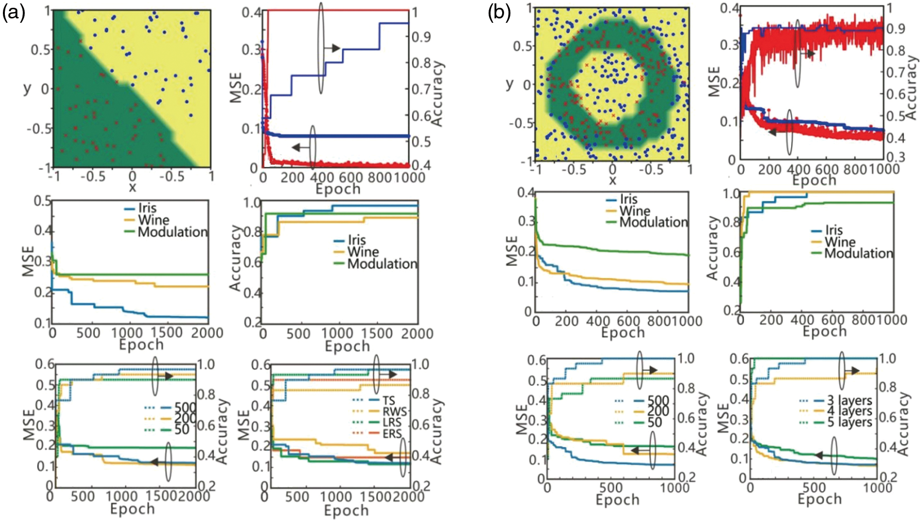
Figure 8: Comparison of various schemes. (a) Using genetic algorithm, (b) using PSO
Nonlinear operations have become another bottleneck in the development of photonic neural networks because it is more difficult to produce nonlinear functions in optoelectronic devices than in electrical devices, and the nonlinear functions achieved have numerous non-ideal properties. However, the nonlinear function in the neural network may increase the network’s convergence speed and enhance recognition accuracy, making it an essential component of the network. At present, the implementation of nonlinear operations in photonic neural networks mainly uses saturable absorbers or circuit simulation, but some of these methods are difficult to control accurately, and some also require the translation of optical impulses into electrical signals via photodiodes, which slows down calculating speed.
At present, the most studied all-optical nonlinear computing element is the saturable absorber. The principle of using the saturable absorber as the nonlinear operation element is to use the transmission characteristic curve of the saturable absorber as the activation function in the neural network. As the peak light intensity of the incident pulse increases, the absorption coefficient of the saturable absorber gradually decreases, which increases the light transmittance. In [45], the authors obtained the transmission characteristic curve of the saturable absorber through simulation. This curve can be used to approximate and simulate widely used nonlinear functions in neural networks. After the Seldon model was proposed, researchers further studied the nonlinear characteristics of saturable absorbers and tried to apply them to the nonlinear part of feedforward and recurrent neuralnetworks [46,47].
In 2019, reference [48] proposed an optoelectronic hybrid controllable nonlinear operation module, the basic structure of which is shown in Fig. 9a. The module consists of a directional coupler delay line, MZI, photodiode, amplifier, bias voltage source, and electrical transmission module. The input optical signal carrying the linear calculation results is divided into two paths by a directional coupler; one path is transmitted to the input arm of the MZI through a delay line, and the other path is converted into an electrical signal through a photodiode, which is processed and biased in the electrical domain. The voltages together control the phase of the phase shifter on the MZI, and the final interference result is output from one arm of the MZI. As shown in Fig. 9b, the nonlinear function can be changed by adjusting the voltage of the phase shifter, thereby realizing the reconfigurability of the nonlinear module.
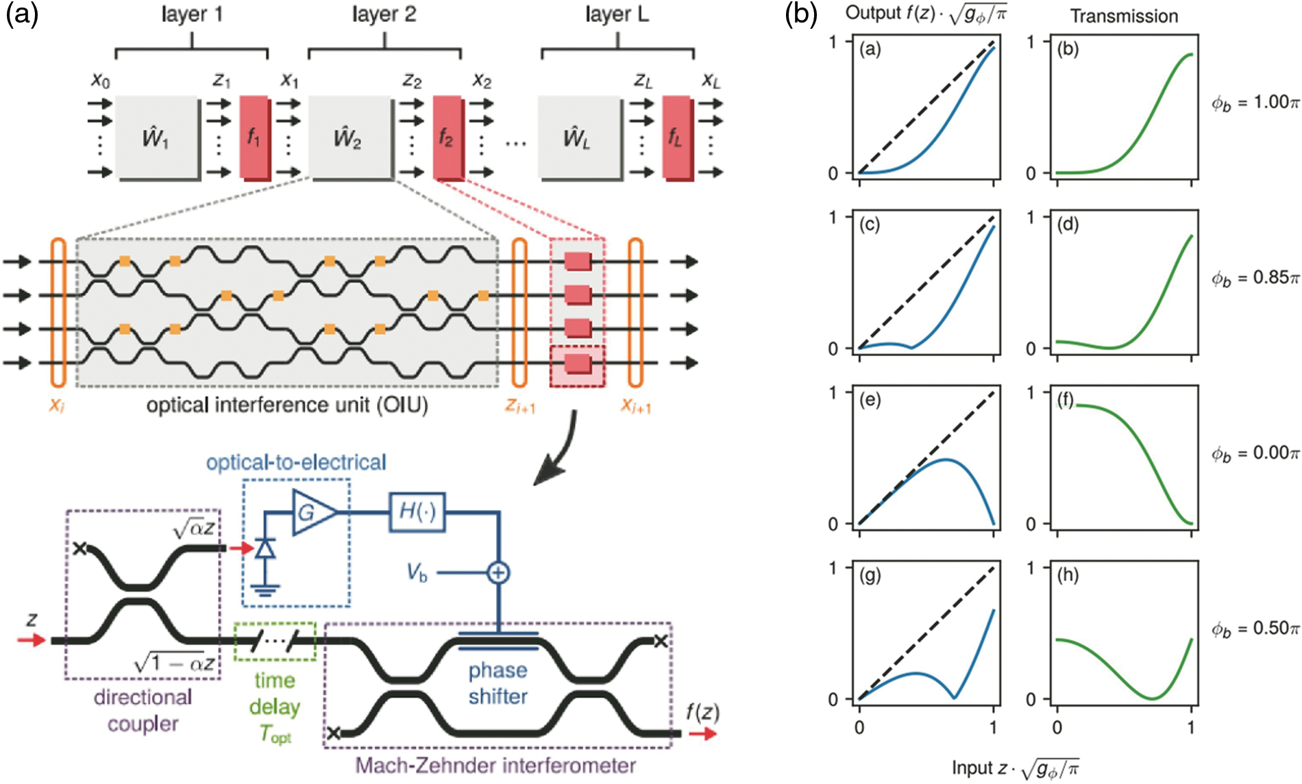
Figure 9: MZI architecture. (a) Nonlinear module, (b) nonlinear functions
In addition to the two systems mentioned above, reference [49] suggested a light-controlled phase-change memory (PCM) scheme and utilized it to implement photonic neurons’ nonlinear transformation. PCM which is regulated by working state light. The operating condition of the material is between crystalline and amorphous and is controlled by the optical power input. When the input optical power is less than the threshold power, as shown in Fig. 10, and a significant amount of optical light is absorbed, the PCM is in a crystal state. When the input optical power surpasses the threshold power, the PCM enters an amorphous state, enabling the bulk of the optical power to pass through. The optical permeability of the material may be adjusted in response to the input optical power as a consequence of integrating the material into the optical transmission medium, accomplishing the function of the photonic neural network’s nonlinear activation function.
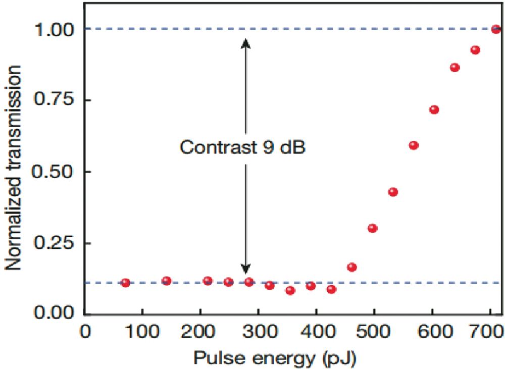
Figure 10: Comparison of normalized transmission and pulse energy phase-change memory method
Two-dimensional graphene materials are also expected to be used to realize optical activation functions [50–53]. Compared with traditional saturable absorbers, graphene has the characteristics of a low threshold, easy excitation, and rich nonlinear effects. At present, research on optical nonlinear materials and devices is underway [54,55], and the research goals focus on four aspects: low threshold, reconfigurability, easy integration, and fast response.
3.3 Scaling of Photonic Neural Networks
The scale of the photonic neural network is another difficult problem to solve. On the one hand, large-scale neural networks are beneficial to realize more complex functions; on the other hand, the unstable and difficult fine-tuning characteristics of photonic devices make it difficult to expand the scale of neural networks. To solve this problem, reference [56] proposed a diffraction-based photonic deep neural network (D2NN) structure in 2018, which not only realized the classification function of handwritten digits and fashion datasets but also improved the spatial imaging resolution. Fig. 11a depicts the structure of the diffraction-based photonic DNN. The photonic deep neural network realizes linear operation based on the Huygens principle and uses light diffraction superposition. The principle realizes the connection between two adjacent layers of neurons. When in use, coherent light is incident on the “phase modulation” plate in parallel. Each pixel block on the “phase modulation” board is equivalent to a neuron, and the pixel blocks in different positions communicate with each other. By changing the thickness, the phase difference when the light passes through is changed, so that there are different weights between different nodes. After such a series of transmissions, the output of the deep neural network can be obtained by counting the received results of the PD placed at a specific position. Since the “phase modulation” plate has hundreds of pixels, the neural network with this structure is adopted. The number of nodes in each layer can be expanded to several hundred. Fig. 11b depicts the improvement of spatial imaging resolution.
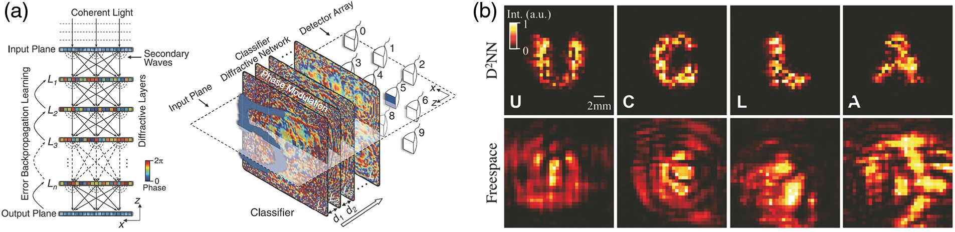
Figure 11: Diffraction-based photonic deep neural network. (a) Architecture, (b) improvement of images
Time may be traded for space to grow the dimension of the photonic neural network, and the size of the neural network can be expanded serially without lowering operating speed. Reference [57] proposed a time domain stretching-based serial PNN which is shown in Fig. 12. The broad-spectrum pulse output from the laser is dispersion broadened and spectrally shaped by the large-dispersion module, and the subsequent modulator modulates the input and configuration of each layer onto the optical pulse, respectively. After passing through the dispersion compression module and the photodiode, the energy of the optical pulse carrying the information is compressed and accumulated, and finally, the calculation result of vector multiplication and addition is obtained. The optoelectronic hybrid, fully connected neural network is realized using a parallel-to-serial strategy in this method. Using this scheme, a large-scale neural network can be realized. Theoretically, the number of neural network nodes that can be simulated by a single stretched optical pulse depends on the width of the stretched optical pulse and the maximum simulated bandwidth of the arbitrary waveform generator. Using this structure, a neural network with three layers, each containing 400, 23, and 10 neurons, was verified by the simulation to realize the function of handwritten digit recognition. Figs. 13a–13c show the confusion matrix of the traditional electrical neural network structure in the case of no noise and with noise, and the recognition accuracy is 94%, 89%, and 88%, respectively.
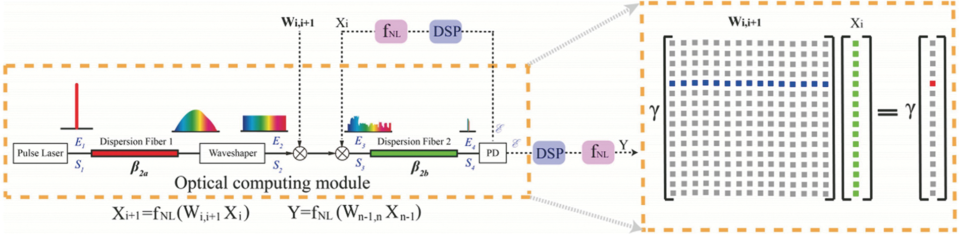
Figure 12: Architecture of time-domain stretching
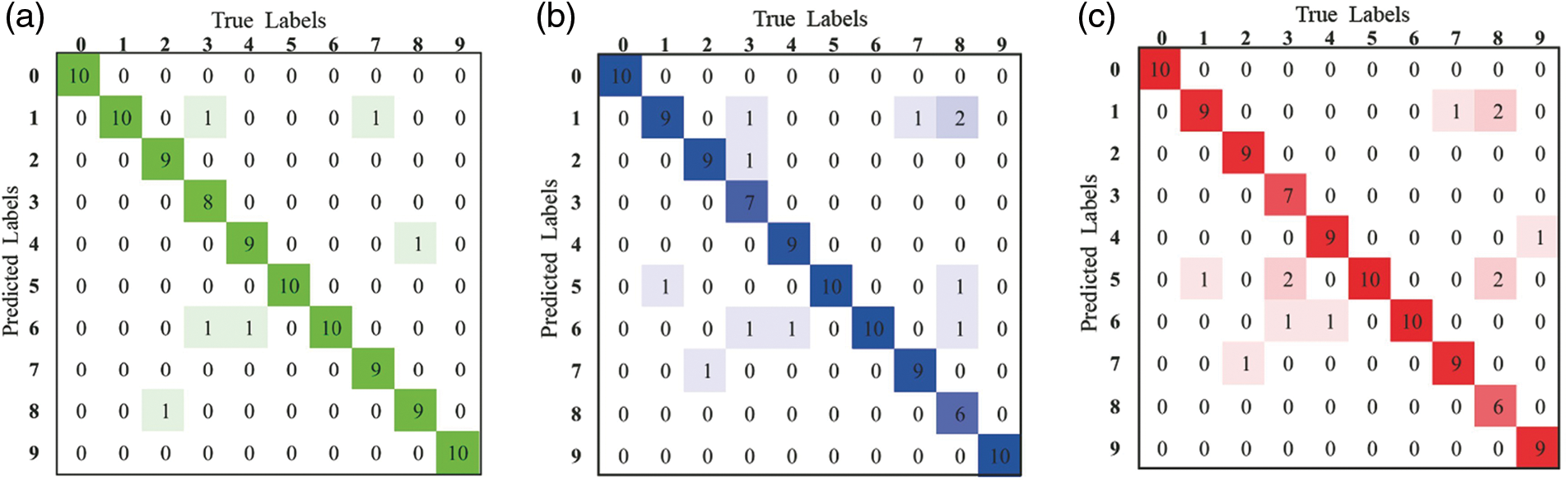
Figure 13: Comparison of matrices of neural networks. (a) Traditional NN, (b) time-domain stretching without noise, (c) time-domain stretching with noise
Another trend in the development of photonic neural networks is practicality. However, limited by the scale and complexity of existing photonic neural networks, the practical application of photonic neural networks still needs a long development time. In the field of communication and data processing, to fulfill the equalization function of the communication channel, reference [28] used a hybrid RNN based on an optical fiber system. In addition, thanks to the advantages of recurrent neural networks in the regression analysis of time series signals, optical storage pool computing have been initially applied in financial sequence forecasting and sequential signal processing. In the field of optical communication, the authors implemented a binary optical coherent receiver by using an optoelectronic hybrid network and realized the recovery of the modulated signal at the transmitter [58]. Its structure is shown in Fig. 14a. After being input from the input layer, the optical signal modulated by quadrature phase shift keying (QPSK) is processed by a binary all-optical neural network, followed by a photodiode and an analog-to-digital converter. It is converted into an electrical signal, and finally, the original modulated signal is restored by an electrical artificial neural network. It proposed two structures to achieve binary weight mapping in the optical domain for single-polarization and polarization multiplexing systems, respectively, as shown in Figs. 14b–14c. The balanced photodiode realizes the linear computing unit of the binary neural network. The activation function of the binary neural network is realized by using a balanced photodiode and an analog-to-digital converter (ADC) with a 1-bit vertical resolution. The electrical signal passing through the balanced photodiode and ADC is processed by the electrical neural network, and finally, the transmission signal can be realized.
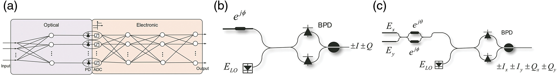
Figure 14: Illustrations of binary NN. (a) Architecture, (b) single polarization mapping, (c) multiplexing polarization mapping
It can be seen from the simulation that the optoelectronic hybrid binary neural network realizes a 50 Gb/s single-polarization SP-QPSK signal receiver and a 100 GB/s polarization multiplexing QPSK signal receiver, respectively. According to the laser linewidth (0, 100 Hz) and the realization method (traditional receiver, optoelectronic hybrid binary neural network), the bit error rate (BER)-optical signal as shown in Figs. 15a and 15b is obtained. The simulation results show that the binary coherent receiver can be used in coherent optical communication systems, and the neural network calculation in the optical domain can relieve the signal processing pressure in the electrical domain, reduce the power consumption of the overall optical receiver, and improve the signal processing speed of the optical receiver. In addition, the binary neural network can greatly reduce the requirement for the number of quantization bits of the analog-to-digital converter, so that only the analog-to-digital converter with 1-bit quantization can realize the recovery of complex debugging format signals, which greatly reduces the optical receiver.
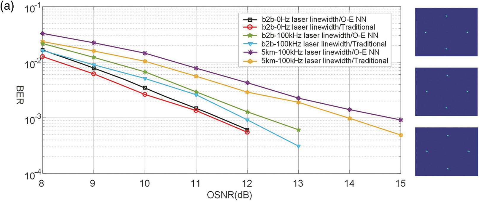
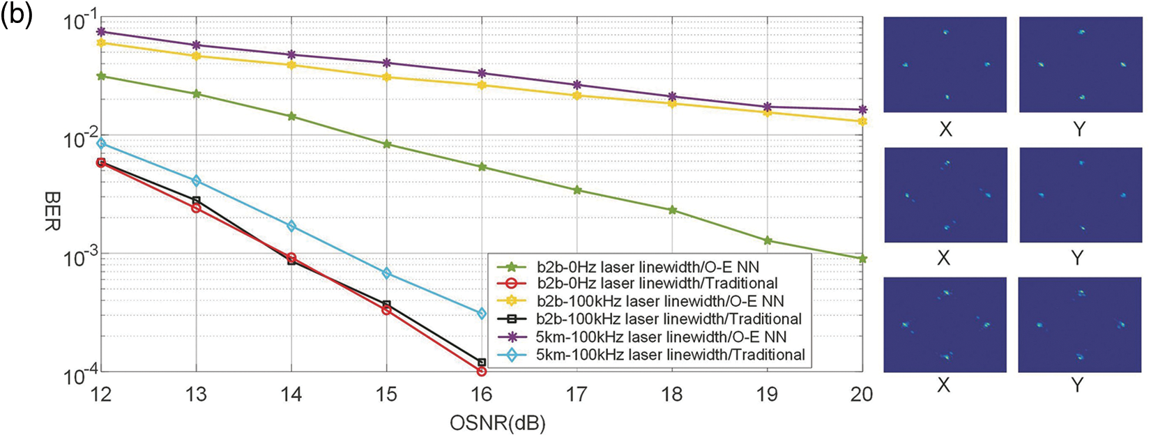
Figure 15: Comparison of algorithms’ bit-error rate. (a) QPSK with single polarization, (b) QPSK with multiplexed polarization
This paper provides a comparative performance evaluation of various models for optical neural networks. Photonic neural networks, being a transdisciplinary result of optical (electrical) technology and artificial intelligence technology, may use the benefits of both to build a high-speed, low-power network structure that avoids the bottleneck that plagues traditional electronic neural networks. Benefiting from the maturity and development of optoelectronic device manufacturing technology, especially the development of integrated optoelectronic technology, photonic neural network technology has made breakthroughs in the construction of feedforward, recurrent, and spiking neural networks using optoelectronic devices. However, the photonic neural network still has a lot of potential for growth in terms of trainability, integration, size, and practicality when compared to the recently existing electronic neural network. On the one hand, the non-ideal and unstable performance of optoelectronic devices hinders the trainability, integration, and scalability of photonic neural networks, requiring stricter requirements for developing neural network models with increasingly complicated functionalities. In the application field, however, the photonic neural network is likewise constrained by the aforementioned effects, making it impossible to fully use its advantages in certain domains. Although various solutions have been presented in recent years, how to break through the photonic neural network barrier from the root still requires in-depth thought and study. It is expected that, in the not-too-distant future, the photonic neural network will be able to overcome these challenges, better exploit the advantages of high speed and low power consumption brought by optoelectronic and artificial intelligence technology, and better build a green and intelligent world.
Acknowledgement: The authors would like to thanks Princess Nourah Bint Abdulrahman University for their support.
Funding Statement: The authors extend their appreciation to the Deputyship for Research & Innovation, Ministry of Education in Saudi Arabia for funding this research work through Project Number RI-44-0345.
Author Contributions: The authors confirm contribution to the paper as follows: study conception and design: Z. Lv, I. Khan; data collection: S. Sefat; analysis and interpretation of results: A. Alhussan,D. Khafaga; draft manuscript preparation: Z. Lv, I. Khan. All authors reviewed the results and approved the final version of the manuscript.
Availability of Data and Materials: The data used for the findings of this study are available within this article.
Conflicts of Interest: The authors declare that they have no conflicts of interest to report regarding the present study.
References
1. S. Jeon, A. Elsharkawy and M. Kim, “Lipreading architecture based on multiple convolutional neural networks for sentence-level visual speech recognition,” Sensors, vol. 22, no. 1, pp. 1–19, 2022. [Google Scholar]
2. M. Qizwani, I. Barjasteh and H. Al-Qassab, “Deep learning algorithm for autonomous driving using googlelenet,” in IEEE Intelligent Vehicles Symp., Los Angeles, USA, pp. 87–96, 2017. [Google Scholar]
3. W. Zhou and F. Zhou, “Priority-ware resource scheduling for UAV-mounted mobile edge computing networks,” IEEE Transactions on Vehicular Technology, vol. 8, no. 3, pp. 1741–1753, 2023. [Google Scholar]
4. L. Chen and X. Lei, “Relay-assisted federated edge learning: Performance analysis and system optimization,” IEEE Transactions on Communications, vol. 3, no. 5, pp. 1078–1091, 2023. [Google Scholar]
5. W. Zhou and F. Zhou, “Profit maximization for cache-enabled vehicular mobile edge computing networks,” IEEE Transactions on Vehicular Technology, vol. 9, no. 8, pp. 1667–1679, 2023. [Google Scholar]
6. X. Zheng, F. Zhu and J. Xia, “Intelligent computing for WPT-MEC-aided multi-source data stream,” EURASIP Journal on Advanced Signal Processing, vol. 23, no. 44, pp. 1–19, 2023. [Google Scholar]
7. J. Ling, J. Xia and F. Zhu, “DQN-based resource allocation for NOMA-MEC-aided multi-source data stream,” EURASIP Journal on Advances in Signal Processing, vol. 23, no. 44, pp. 1–18, 2023. [Google Scholar]
8. Y. Wu and C. Gao, “Intelligent resource allocation scheme for cloud-edge-end framework aided multi-source data stream,” EURASIP Journal on Advances in Signal Processing, vol. 23, no. 1018, pp. 1–16, 2023. [Google Scholar]
9. L. He and X. Tang, “Learning-based MIMO detection with dynamic spatial modulation,” IEEE Transactions on Cognitive Communications and Networking, vol. 5, no. 2, pp. 1337–1345, 2023. [Google Scholar]
10. J. Dang, J. Gao, Z. Zhang, L. Wu, B. Zhu et al., “Performance of optical mobile communications with user mobility and multiple light sources,” Wireless Communications and Mobile Computing, vol. 21, pp. 1–14, 2021. [Google Scholar]
11. G. Balasubramanian, B. Wiesel, N. Biton, R. Kumar, J. Kupferman et al., “Tutorial on the use of deep learning in diffuse optical tomography,” Electronics Journal, vol. 11, no. 3, pp. 1–18, 2022. [Google Scholar]
12. V. Ussyshkin and L. Theriault, “Airborne lidar: Advances in discrete return technology for 3d vegetation mapping,” Remote Sensing Journal, vol. 3, no. 3, pp. 1–17, 2011. [Google Scholar]
13. M. Saruwatari, “All-optical signal processing for terabit/second optical transmission,” IEEE Journal of Selected Topics in Quantum Electronics, vol. 6, no. 6, pp. 1363–1374, 2000. [Google Scholar]
14. L. Brzozowski and E. Sargent, “Optical signal processing using nonlinear distributed feedback structures,” IEEE Journal of Quantum Electronics, vol. 36, no. 5, pp. 550–555, 2000. [Google Scholar]
15. J. Cao, K. Udhayakumar, R. Rakkiyappan, X. Li and J. Li, “A comprehensive review of continuous-/discontinuous-time fractional-order multidimensional neural networks,” IEEE Transactions on Neural Networks and Learning Systems, vol. 8, no. 3, pp. 1–21, 2021. [Google Scholar]
16. K. Udhayakumar, F. Rihan, X. Li and R. Rakkiyappan, “Quasi-bipartite synchronization of multiple inertial signed delayed neural networks under distributed event-triggered impulsive control strategy,” IET Control Theory & Applications, vol. 15, no. 12, pp. 1615–1627, 2021. [Google Scholar]
17. U. Kandasamy and R. Rajan, “Hopf bifurcation of a fractional-order octonion-valued neural networks with time delays,” Discrete & Continuous Dynamical Systems-Series, vol. 13, no. 9, pp. 2537–2559, 2020. [Google Scholar]
18. J. Escarten, V. Gimeno and J. Fernandez, “Optimal approximation to unitary quantum operators with linear optics,” Quantum Information Processing, vol. 20, pp. 265–276, 2021. [Google Scholar]
19. A. Ribeiro, A. Ruocco and L. Vanacker, “Demonstration of a 4 * 4-port universal linear circuit,” Optica, vol. 3, no. 12, pp. 1348–1357, 2016. [Google Scholar]
20. W. Clements, P. Humphreys and B. Metcalf, “Optimal design for universal multiport interferometers,” Optika, vol. 3, no. 12, pp. 1460–1465, 2016. [Google Scholar]
21. Y. Shen, N. Harris, S. Skirlo and X. Kim, “Deep learning with coherent nanophotonic circuits,” Nature Photonics, vol. 11, no. 7, pp. 1071–1085, 2017. [Google Scholar]
22. X. Xu, L. Zhu, W. Zhuang, L. Lu and P. Yuan, “A convolution neural network implemented by three 3 × 3 photonic integrated reconfigurable linear processors,” Photonics Journal, vol. 9, no. 2, pp. 1–16, 2022. [Google Scholar]
23. G. Tanaka, T. Yamane, J. Heroux, R. Nakane, N. Kanazawa et al., “Recent advances in physical reservoir computing: A review,” Neural Networks, vol. 115, no. 3, pp. 100–123, 2019. [Google Scholar] [PubMed]
24. W. Du, C. Li, Y. Huang, J. Zou, L. Luo et al., “An optoelectronic reservoir computing for temporal information processing,” IEEE Electron Device Letters, vol. 43, no. 3, pp. 406–409, 2022. [Google Scholar]
25. A. Rohm, L. Jaurigue and K. Ludge, “Reservoir computing using laser networks,” IEEE Journal of Selected Topics in Quantum Electronics, vol. 26, no. 1, pp. 1–8, 2020. [Google Scholar]
26. K. Vandoorne, J. Dambre and D. Verstraeten, “Parallel reservoir computing using optical amplifiers,” IEEE Transactions on Neural Networks, vol. 22, no. 9, pp. 1469–1481, 2011. [Google Scholar] [PubMed]
27. J. Bueno, S. Maktoobi, L. Froehly and A. Kloub, “Reinforcement learning in a large-scale photonic recurrent neural network,” Optica, vol. 5, no. 6, pp. 756–760, 2018. [Google Scholar]
28. Y. Paquot, F. Duport and A. Smerieri, “Optoelectronic reservoir computing,” Scientific Reports, vol. 2, no. 287, pp. 1–23, 2012. [Google Scholar]
29. F. Duport, B. Schneider and A. Smerieri, “All-optical reservoir computing,” Optics Express, vol. 20, no. 20, pp. 22783–22795, 2012. [Google Scholar] [PubMed]
30. H. Zhang, X. Feng, B. Li and S. Zhu, “Integrated photonic reservoir computing based on hierarchical time-multiplexing structure,” Optics Express, vol. 22, no. 25, pp. 3135–3147, 2014. [Google Scholar]
31. W. Maass, “Networks of spiking neurons: The third generation of neural network models,” Neural Networks, vol. 10, no. 9, pp. 1659–1671, 1997. [Google Scholar]
32. B. Shastri, M. Nahmias, A. Tait, A. Rodriguez, B. Wu et al., “Spike processing with a graphene excitable laser,” Scientific Reports, vol. 6, no. 2, pp. 19126–19135, 2016. [Google Scholar] [PubMed]
33. T. Peng, M. Nahmias and T. Lima, “Neuromorphic photonic integrated circuits,” IEEE Journal of Selected Topics in Quantum Electronics, vol. 24, no. 6, pp. 1–15, 2018. [Google Scholar]
34. A. Tait, M. Nahmias, B. Shastri and P. Pruncal, “Broadcast and weight: An integrated network for scalable photonic spike processing,” Journal of Lightwave Technology, vol. 32, no. 21, pp. 4029–4041, 2014. [Google Scholar]
35. S. Bohre, J. Kok and H. Lapoutre, “Error-backpropagation in temporally encoded networks of spiking neurons,” Neurocomputing Journal, vol. 48, no. 1, pp. 17–32, 2002. [Google Scholar]
36. R. Gutig and H. Sompolinsky, “The tempotron: A neuron that learns spike timing-based decisions,” Nature Neuroscience, vol. 9, no. 3, pp. 420–428, 2006. [Google Scholar] [PubMed]
37. S. Song, K. Miller and K. Abbort, “Competitive hebbian learning through spike-timing-dependent synaptic plasticity,” Nature Neuroscience, vol. 3, no. 9, pp. 919–926, 2000. [Google Scholar] [PubMed]
38. F. Ponulak and A. Kasinski, “Supevised learning in spiking neural networks with resume: Sequence learning, classification, and spike shifting,” Neural Computation, vol. 22, no. 2, pp. 467–510, 2010. [Google Scholar] [PubMed]
39. A. Mohemmed, S. Schliebs and S. Matsuda, “Span: Spike pattern association neuron for learning spatio-temporal spike patterns,” International Journal of Neural Systems, vol. 22, no. 4, pp. 1053–1067, 2012. [Google Scholar]
40. Q. Yu, H. Tang and K. Tan, “Precise-spike-driven synaptic plasticity: Learning hetero-association of spatiotemporal spike patterns,” PLoS One, vol. 8, no. 11, pp. 1–16, 2013. [Google Scholar]
41. T. Hughes, M. Minkov, Y. Shi and C. Shen, “Training of photonic neural networks through in situ backprogation and gradient measurment,” Optica, vol. 8, no. 11, pp. 73–85, 2013. [Google Scholar]
42. T. Zhang, J. Wang and Y. Dan, “Efficient training and design of photonic neural network through neuroevolution,” Optics Express, vol. 27, no. 26, pp. 3710–3727, 2019. [Google Scholar]
43. D. Al-Nuaimi, I. Hashim, I. Abidin, L. Salman and N. Matisa, “Performance of feature-based techniques for automatic digital modulation recognition and classification–A review,” Electronics Journal, vol. 8,no. 12, pp. 1–15, 2019. [Google Scholar]
44. Y. Gao, N. Xu and W. Xu, “The mpsk and mqam signal modulation recognition algorithm in the multipath channel,” International Journal of Electronics, vol. 106, no. 1, pp. 1–12, 2017. [Google Scholar]
45. B. Kim, S. Hong, J. Park, Y. Dong and K. Oh, “All-fiber integrated saturable absorber-tunable wavelength filter for Q-switching laser in both C-and L-bands,” Optics Express, vol. 29, no. 9, pp. 13183–13192, 2021. [Google Scholar] [PubMed]
46. A. Dejonckheere, F. Duport and A. Smerieri, “All-optical reservoir computer based on saturation of absorption,” Optics Express, vol. 22, no. 9, pp. 1068–1079, 2014. [Google Scholar]
47. Y. Gao, X. Zhang and Y. Li, “Saturable absorption and reserve saturable absorption in platinum nanoparticles,” Optics Communications, vol. 251, no. 6, pp. 429–433, 2005. [Google Scholar]
48. I. William, T. Hughes and M. Minkov, “Reprogrammable electro-optic nonlinear activation functions for optical neural networks,” IEEE Journal of Selected Topics in Quantum Electronics, vol. 26, no. 1, pp. 1–12, 2020. [Google Scholar]
49. J. Feldmann, N. Youngblood and C. Wright, “All-optical spiking neurosynaptic networks with self-learning capabilities,” Nature Journal, vol. 569, no. 7755, pp. 208–214, 2019. [Google Scholar]
50. Q. Bao, H. Zhang, Z. Ni and Q. Zhang, “Monolayer graphene as a saturable absorber in a mode-locked laser,” Nano Research, vol. 4, no. 3, pp. 297–307, 2011. [Google Scholar]
51. G. Lim, Z. Chen and J. Clark, “Giant broadband nonlinear optical absorptionresponse in dispersed graphene single sheets,” Nature Photonics, vol. 5, no. 9, pp. 554–560, 2011. [Google Scholar]
52. X. Hu, A. Wang, M. Zeng and Q. Chen, “Graphene-assisted multiple-input high-base optical computing,” Scientific Reports, vol. 6, no. 4, pp. 3291–3305, 2016. [Google Scholar]
53. R. Yadav, J. Aneesh and R. Sharma, “Designing hybrids of graphene oxide and gold nanoparticles for nonlinear optical response,” Physical Review Applied Journal, vol. 9, no. 4, pp. 976–988, 2018. [Google Scholar]
54. M. Miscuglio, A. Mehrabian and Z. Hu, “All-optical nonlinear activation function for photonic neural networks,” Optical Materials Express, vol. 8, no. 12, pp. 3851–3864, 2018. [Google Scholar]
55. B. Yen, M. Hoang, X. Dong and T. Lu, “Universal activation function for machine learning,” Scientific Reports, vol. 11, no. 3, pp. 18757–18768, 2021. [Google Scholar]
56. X. Lin, Y. Rivension and N. Yardimci, “Allp-optical machine learning using diffractive deep neural networks,” Science Journal, vol. 361, no. 6406, pp. 1004–1008, 2018. [Google Scholar]
57. Y. Zang, M. Chen, S. Yang and Z. Wang, “Electro-optical neural networks based on time-stretch method,” IEEE Journal of Selected Topics in Quantum Electronics, vol. 26, no. 1, pp. 1–10, 2020. [Google Scholar]
58. Z. Yu, X. Zhao, S. Yang, W. Shen and K. Zhou, “Binarized coherent optical receiver based on opto-electronic neural network,” IEEE Journal of Selected Topics in Quantum Electronics, vol. 26, no. 1, pp. 1–9, 2020. [Google Scholar]
Cite This Article
 Copyright © 2023 The Author(s). Published by Tech Science Press.
This work is licensed under a Creative Commons Attribution 4.0 International License , which permits unrestricted use, distribution, and reproduction in any medium, provided the original work is properly cited.
 Downloads
 Citation Tools