
 Submit a Paper
 Propose a Special lssue
 Open Access
ARTICLE

A Universal BIST Approach for Virtex-Ultrascale Architecture
1 CSI College of Engineering, Ketti, 643215, Tamilnadu, India
2 Sri Ramakrishna Institute of Technology, Coimbatore, 641010, Tamilnadu, India
* Corresponding Author: N. Sathiabama. Email:
Computer Systems Science and Engineering 2023, 45(3), 2705-2720. https://doi.org/10.32604/csse.2023.025941
Received 10 December 2021; Accepted 14 June 2022; Issue published 21 December 2022
 View Full Text
 Download PDF
Abstract
Interconnected cells, Configurable Logic Blocks (CLBs), and input/output (I/O) pads are all present in every Field Programmable Gate Array (FPGA) structure. The interconnects are formed by the physical paths for connecting the blocks . The combinational and sequential circuits are used in the logic blocks to execute logical functions. The FPGA includes two different tests called interconnect testing and logical testing. Instead of using an additional circuitry, the Built-in-Self-Test (BIST) logic is coded into an FPGA, which is then reconfigured to perform its specific operation after the testing is completed. As a result, additional test circuits for the FPGA board are no longer required. The FPGA BIST has no area overhead or performance reduction issues like conventional BIST. A resource-efficient testing scheme is essential to assure the appropriate operation of FPGA look-up tables for effectively testing the functional operation. In this work, the Configurable Logic Blocks (CLBs) of virtex-ultrascale FPGAs are tested using a BIST with a simple architecture. To evaluate the CLBs’ capabilities including distributed modes of operation of Random Access Memory (RAM), several types of configurations are created. These setups have the ability to identify 100% stuck-at failures in every CLB. This method is suitable for all phases of FPGA testing and has no overhead or performance cost.Keywords
The significance of FPGA is extremely remarkable in various applications because it possesses variety of beneficial measures like robust structure, high flexibility, easy upgradability, innovative functuning and maximum efficiency. As the durability of FPGA is high, it is preferred by the manufacturers in various applications. Unlike the Application Specific Integrated Circuits (ASICs), which are customized by the manufacturer, the FPGA is configured in the field by the user. The CLBs and RAMs are used to implement combinational and sequential logic functions in FPGAs [1,2]. Furthermore, certain FPGAs are partially reprogrammed in the runtime to perform the implementation of reconfigurable hardware circuits. Because of having the feature of high versatility, the FPGAs are highly demanded in the fields like defense and space exploration. In spite of having these advantageous elements, the operation of FPGA gets distorted when it is subjected to the extreme environmental conditions like shorter wavelengths, which is regarded as one of the major limitations of FPGA [3,4]. Thus, it is highly mandatory to test the FPGA before the programming process as it is broadly employed in mission-critical applications.
As the FPGA testing includes testing of logic functions and interconnections, it becomes a difficult task [5,6]. Hence, new testing methods are developed to reduce the cost of overhead circuitry and testing time along with the boosting of fault coverage. Generally, the testing is done by applying a test vector to the circuit and comparing the results to the predicted results [7,8]. However, large test vectors are required to test a circuit when the feature sizes are decreased and device complexity is increased. In addition, an external circuit is required for storing all the test setups, which is actually a major downside of this testing approach [9]. By testing the on board circuit components of FPGA, the limitations of employing large test vectors and external circuits are overcome by the modular tesing of embedded cores, which is highly advantageous in terms of the testing time [10]. In spite of having an beneficial element, it has certain limitations, which are rectified by BIST scheme.
With the increasing complication of Very Large Scale Integration (VLSI) devices, the necessity of cost-effective testing approach such as the BIST grows [11,12]. The BIST is good enough in dealing with the faults like transition fault, address decoder fault, stuck-at fault, neighborhood pattern sensitive fault and coupling fault. The BIST architecture is significantly portrayed in Fig. 1.

Figure 1: BIST architecture
The Test Pattern Generator (TPG), Circuit Under Test (CUT) and Output Response Analyzer (ORA) are the components of a basic BIST method. The goal of BIST is to create a circuit for checking whether it is under fault or fault-less condition and to continue the function even if the testing is taken place [13].
The TPG acts as a stimulus for the CUT and it generates a pattern series, which causes the CUT to produce the desired output. The ORA examines the CUT’s outcome and generate a ride indicator by depending on the the expected or incorrect output. The Circuits like isolation circuit and a test controller are required for the system level implementation. The isolation circuitry is a 2:1 multiplexer, which alternates between the typical and BIST operations. To avoid any untested data from accessing ORA, the test controller ensures that all modules in the BIST circuit are activated. The BIST method includes an output bit that communicates the system’s state (pass/fail) to an output source. To indicate the start and finish operation of a test sequence, the commence and end flags are utilized in the BIST. The number of faults discovered is analogised with the total possible defects count of the system (fault coverage) and the effectiveness of a BIST test is defined by test time [14–16].
The key benefits of BIST are clearly presented in the subsequent sectionas,
• The vertical testability validates a device at any level of production.
• It seems to be a less expensive technique than the external testing [17].
• For at-speed testing, the BIST employs the system’s internal clock, which allows it to discover components that cause excessive delay in a functional circuit.
• As the testing is done at a high speed, it helps to cut down on test time.
• With BIST, the user can test the circuit in the field [18–20].
• Detecting un-modeled flaws in a circuit is easier with pseudorandom patterns.
The CLBs, Programmable Interconnects (PIs), Input/ Output Buffers (IOBs) and RAM cores are the components of FPGA. For improving the system performance, the FPGAs are employed with extra integrated cores like Digital Signal Processor (DSP), embedded processors and high-speed I/O devices. The Look up Tables (LUTs) make up CLBs whereas the flipflops make up the logic portion of an FPGA. The wires and switches connect or disconnect the wire segments to create a programmable interconnect network [21–23]. These programmable interconnect networks surround the CLBs and allows the CLB blocks to be interlinked. The CLBs are encircled by IOBs, which interconnect the chip with the rest of the world.
For Xilinx FPGAs, the CLBs supply the basic logic elements. These CLBs offer combinational and synchronous logic along with the distributed memory and SRL16 shift register functionality [24]. The CLBs are the primary sources to implement logical circuits. Each CLB is hooked to a switched matrix to access the route matrix. Four slices make up a CLB element. These slices are arranged in a column and grouped in pairs. The SLICEM consists of a slices pair in the left column whereas the SLICEL consists of a slices pair in the right column. In the column, each pair has its own carry chain [25]. Only the slices in SLICEM share a general shift chain. For Xilinx FPGAs, the CLBs supply the basic logic elements. The CLBs have distributed memory, SRL16 shift register functionality, combinatorial and synchronous logic. The Ultra-Scale architecture’s CLB is efficiently illustrated in Fig. 2.

Figure 2: CLB of ultra-scale architecture
2 Overview of Virtex-Ultrascale Architecture
The CLBs with six-input LUTs, configurable latches/flip-flops, multipliers (27 × 18), RAM blocks (36 Kb) with inbuilt First In First Out (FIFO), error correction code memory and 4K × 72 block Ultra-RAM are linked through a less interlude high performance interconnect.
To evaluate the extremely capable and programmable RAM blocks, the CLBs include multiplexer, shift register, and carry logic features with additional option to set the LUT as proportioned memory [26]. With 96-bit length XOR capabilities, 27-bit adder, and 30-bit input, the DSP slice independently executes a variety of operations such as accumulated multiplication, multiple add and pattern detect. The signals pass among the Super-Logic Regions (SLRs) via specialized, low-interlude interface in devices implemented with SSI technology. This combination of routing resources makes it simple to handle next-generation bus data widths. Up to 16 GB of high bandwidth memory is available in these devices.
These devices have strong clock management circuits such as clock synthesis, buffers, and routing modules, which work together to create a highly capable framework for satisfying the design requirements.
Similar to the 7-series slices capacity, the UltraScale CLB has single and coarser slice. The LUTs and operations have preserved the functionality. The LUT-op-pairs of the UltraScale CLB is shown in Fig. 3.

Figure 3: Logic elements of ultra-scale architecture
This UltraScale CLB provides immediate permission to all CLB operations without using the LUTs as it has the same number of bypass inputs. In addition, each slice has its own set of parallel and separate output pin that is linked to the switched matrix. The usage of more pins is normally costly as the switch matrix has to be resized to fit the new pins. However, this expense is spread out among the remaining pins in UltraScale. The interconnection connects each CLB with 64 inputs and 32 outputs.
Memory and shift register operating modes are also supported by some slices. Each slice’s LUT RAM has its own read inputs but with divided write memory terminals. The separate read inputs make it easier to build dual-port RAM inside the slices. The LUT is set-up as either a 64 × 1-bit or 32 × 2-bit RAM. The four LUTs produce a 256 × 1-bit RAM using dynamic multiplexers in each slice. To build a 328 × 8-bit RAM, the 4-LUTs divide 5-read address inputs and use 8-separate data inputs. Each LUT is alternatively used to create a 32 × 1 bit shift register or 16 × 2 bit shift register. The eight LUTs are connected in series to create a 256 × 1-bit shift register or connected in parallel to create a 32 × 16-bit shift register.
2.1 CLB in Virtex-Ultrascale Architecture
In this architecture, each CLB has 8 LUTs and 16 flip-flops. The LUTs set up as a single 6-input LUT with 1-output or two 5-input LUTs with distinct output and shared input. If necessary, the LUTs are kept in a flip-flop. In addition, the CLB comprises of arithmetic carry logic and multiplexers with LUTs and flip-flops to construct larger logic functions.
A slice is present in each CLB. The SLICEL and SLICEM are the two sorts of slices. The SLICEM’s LUTs is set up as 64-bit RAM or 32-bit shift registers. When compared to past-generation CLB devices, the CLBs of this architecture offer more routing and interconnectivity. In addition, it provides more control signals and allows better register packing with higher device usage. Fig. 3 significantly portrays the logic elements of this architecture.
The Ultra-scale CLB is modified to allow for dense packaging. Because of the shorter wire lengths and the ability to use active gating pulse, the power consumption is highly reduced. It enhances the performance while lowering interconnection demand.
Tab. 1. lists out the logic resources available in the CLB. These components are used by SLICEM and SLICEL to provide logical, arithmetic, and ROM functions. SLICEM has two additional features such as distributed RAM and 16-bit data shift register.

The BIST method makes use of FPGAs’ general architecture for comparing the outputs of many identical BUTs by using ORAs based comparison. Until all the BUTs are analogised, the ORAs have no fails and the defects affecting any combination of BUTs are detected. As malfunctioning of TPG allows a faulty BUT to be undetected, the alternating BUTs are driven by several identical TPGs. Because of several identical TPGs, a defective TPG allows some BUTs’ outputs to conflict, which results in failures of ORAs.
Depending on the mode of slice, the CLB BIST layouts are split into two types. The first configuration set executes every CLB of the FPGA through its paces in SliceL (logic) mode. The next set executes each SliceM mode. During the second set of settings, only certain slices that match SliceM (memory) mode are investigated.
The BUTs and ORAs are arranged in alternating columns of CLBs in the SliceL BIST design. The BIST configurations are repeated twice again, this time with the CLBs’ responsibilities reverted back, such that each CLB acts as both BUT and ORA. ORA compare the output of two similarly configured BUTs with the outputs of two neighboring BUTs of the similar row, as illustrated in Fig. 4. The ORA flip-flop latches logic 0 for a mismatch between two identical BUT outputs set. The logic 1 is kept in the ORA and perceived as a flip-flop outcome at the ending of the testing process.

Figure 4: Architecture of circular comparison
Normally, the BIST results are collected through a partially configured read back memory, which involves retrieving the contents of each ORA from the memory. But, a novel ORA architecture is deployed that makes advantage of the CLB’s specific carry logic to build an iterative-OR of the ORA outputs.The Carry-in input, which is the result of the preceding ORA, is selected as a passing result of logic 1 in each ORA .
The first ORA’s carry-in input in the iterative-OR chain is linked to Test-Data-In (TDI), while the last ORA’s output is connected to Test-Data-Out (TDO). When any ORA in the chain fails, logic 0 on the ORA’s output selects the carry chain multiplexer’s logic 1 input, which converts to logic 1 on TDO.
Or, TDO toggles TDI’s state, allowing the integration of the iterative-OR chain to be checked at the ending of the BIST test by toggling TDI and monitoring TDO. The contents of the ORAs are recovered using partially configured read-back memory to discover the location(s) of the failed BUT if the OR chain’s output shows a failure. This provides a single-bit on/off indicator to perform test at quicker time without reducing resolution of fault-tolerant applications.
Fig. 5 depicts the proposed architecture’s interconnection design, which demonstrates the connectivity between CLBs of the BIST component. The TPG creates both LUTs’ addresses and delivers them for testing using CUT. The behavior of CUT is then examined using ORA. To avoid fault masking, each ORA contrasts the output of the present memory that is under test with the same row memories and with the following row.

Figure 5: Interconnection of proposed architecture
Very High Speed Integrated Circuit (VHSIC) Hardware Description Language (VHDL) is used to model the working prototype of a Virtex-UltraScale FPGA. The test is performed using a series of six CLBs so as to improve accuracy and avoid fault masking. The integrated SRAM memory of the proposed FPGA architecture is tested and the results and performance analysis are discussed below.
Initially, simulation is carried out without fault. Then, the memory is infiltrated with the several types of faults. The outputs are compared using their unlatched outputs of RAM modules. As a result, the final output is obtained immediately, with no delay.
The simulation result in the absence of fault Fig. 6 depicts. The write signal should be kept high throughout write operations. The sampled input data, the value ‘0’ is stored in memory locations. As illustrated in Fig. 6, the memory output is in high impedance (blue lines) in the write cycle event, while the incorrect outputs are in an indeterminate state (red lines).

Figure 6: Fault-free operation
The data is retrieved from each location and a ‘1’ will be appended to each location throughout the read process. The write enable signal is now held at ‘0’, signifying that a read operation is taking place. The retrieved data is sent to the ORA which matches the output to the fault-less output and instantly activates the PASS/FAIL indication. The ORA outputs indicate “0000,” to signify a fault-free operation. The procedure is repeated in ascending order.
A HOLD instruction is given to the memory cells once the read-and-write operations are completed. Now, the cells will stay in saturated level, and the cell value will be constant. Many faults are tested using this operation. Fig. 7 depicts the result of HOLD operation.

Figure 7: Hold operation
At address “0101,” a stuck-at 1 fault is established in CLB#3’s LUT. The fault signals indicate an output of “00000100” indicates the fault at CLB#3 when the output of CUT #3 is compared with the identically configured neighboring CUTs output. The ORA output is evidently listed out in Tab. 2.

When “0101” is read by the Memory cell, for a predicted ‘0’ value, it reads a ‘1’, as seen in Fig. 8. ORA gets the output after the value is received and compares it with the neighboring LUT signal. The ORA pass/fail signal gets high when the values are out of sync. The yellow circle depicts this. The sequence “00000100” implies a fault with LUT’s CLB #3.
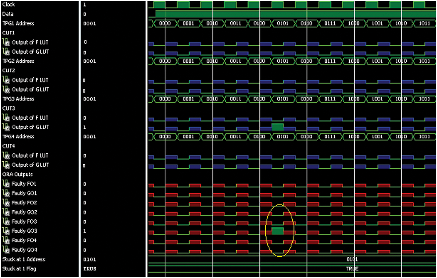
Figure 8: Stuck-at 1 fault at CLB-3
At address “0101” in CLB#3, the “stuck-at 0” issue is established. The memory cell is first viewed as ‘0,’ resulting the viewed output. A ‘1’ is typed into the cell at the end, but the cell is read as ‘1’, it returns a ‘0’. This validates the occurrence of a stuck-at 0 fault, with ORA signals displaying “00001000” for a fault at “0101” address. Fig. 9 depicts the identification of a Stuck-at fault at “0101” address (marked by a yellow circle). The TPG Address is used to point the exact position of the issue, and fault detection requires 33 clock cycles. It takes 33 μs to identify and locate the problem if a clock period is 10 ns (100 MHZ).

Figure 9: Stuck-at 0 fault at CLB-3
This fault is inserted at “0100” address in the CLB #2. Stuck-at 1 fault is introduced to detect the faults when the input lines are stuck-at 1. Fig. 10 shows the detection of address decoder fault at “0100”. When the input of the AND gate is stuck-at ‘1’ and address is “0100”, cell 4 and cell 5 are accessed. During M3 operation, write ‘1’ is performed on cell 5. As more than one cell is accessed with same address, a ‘1’ is also written on cell 4. Thus, when a read operation on cell 4 is performed, it fails and reads a ‘1’ instead. . It takes 59 clock cycles to detect the fault and assuming a clock period of 10 ns, the address decoder fault is detected in 59 μs.

Figure 10: Address decoder fault
A second type of address decoder fault can occur when the cell “0100” is never accessed due to an open gate line. As the cell is never accessed, it shows an ‘X’ (undefined value). Fig. 11 shows the simulation result. It takes 22 clock cycles to detect the fault, and assuming a clock period of 10 ns, the address decoder fault is detected in 22 μs.

Figure 11: Address Decoder fault (due to an open gate line)
Observing the simulation results, the existence of a fault can be identified when the ORA output goes high. The detection of fault is, however, dependent on the type of fault and each fault can be differentiated by the methods explained above and can be uniquely identified. The algorithm requires 12n operations to completely identify the faults. For the 4-input LUT, it requires 128 operations to completely detect the fault and read and write operations are performed in a single clock cycle using both rising and falling edges. Tab. 3 summarizes the time taken to detect a particular fault based on the cell addresses.

To verify the functionality of the CLBs, 25 BIST configurations are constructed (10 for LUT and data-path testing, 2 for shift-register testing). Configured memory bit fault injection method was used to simulate FPGA faults. To represent a fault, the transitional files are purposely damaged to generate the bit-stream configuration. For instance, to represent stuck-at-0 fault in the LUT, the output of a specific LUT is driven to logic-0. Likewise, by changing the associated bit configurations with each resource, the faults are induced in all of the CLB’s logic and memories. ll the faults are detected by the 30 BIST setups. Based on the CLB functionality, the 30 BIST configurations are divided into four categories such as LUT configuration, data-path configuration, shift-register configuration and RAM configuration.
Fig. 12 depicts the group of various configurations’ fault coverage of a CLB. The graph’s left side of Y-axis indicates the total number of faults addressed by each group of configuration, while the right side of Y-axis represents the ratio of faults covered.

Figure 12: Fault coverage
The testing time and the storage needed to hold all BIST configuration is the key overhead involved with FPGA-BIST. The time it takes to upload the BIST configuration to the FPGA is relative to the speed and the overall size of the BIST configurations dominates the test time. The FPGAs’ reconfiguration feature is utilized to minimize overall size of the BIST configuration. The routing information is contained in most of the bits in the bit-stream configuration. As a result, the general routing information is saved in only one bit stream if constant routing is maintained over several bit-streams. For instance, if the first 5 configurations contain similar connection across the consecutive BUTs, indicating that there will be constant routing across all of them. As only the 1st configuration is saved as a full bit stream, a complete bit stream size is 2.6 MB, while the other four are stored as partial bit streams. The required overall memory might be 13 MB if all 5 variants were saved as complete bit streams.
The overall memory required for the five versions is lowered to 4.25 MB by allowing partial bit stream processing. Only 7 of the 30 BIST variants have individual routing, thus only those configurations must be preserved as entire bit streams. As a result of this, the typical bit stream size is lowered by 52%. The FPGA must be partitioned, If all the BUTs couldn’t be addressed in a single arrangement, and each portion must be tested separately. Hence, the number of BIST combinations and the testing duration increase as the partitions increases. The interconnections between the BUTs in the BIST are confined to a short length, hence, all the BUTs might be routed independently. The effective number of BIST configuration is limited, and hence the overheads involved with the BIST are eliminated, since the FPGA is tested without establishing partitions. The test time breakup is clearly shown in Fig. 13.

Figure 13: Test time breakup
The FPGA Comparison outcome is evidently highlighted in Fig. 14 in an efficient manner.

Figure 14: Comparison of FPGA
Tab. 4 validates that the proposed Virtex Ultrascale FPGA is comparatively better than the other FPGA tools because the parameter values on Virtex Ultrascale is greater than the others.

This work presents a comprehensive BIST architecture for detecting and isolating stuck-at-faults or decoder fault in the system. The Virtex Ultrascale FPGA is preferred in this study as it delivers optimal performance with maximum efficiency. For systems that need large data flow and packet processing, it provides a step-function in increased bandwidth and reduced latency. As the test utilizes the configuration interfaces with no external I/O pin, it is used in all system without requiring any Printed Circuit Board (PCB) modifications.The proposed BIST configuration in this study is designed with the use of precise gate-level fault model and tested with configured memory bit fault injection. This BIST design overcomes the problem of congestion in routing of complex devices and allows all the CLBs to be tested in a single test. Thus, the testing time and the amount of external memory to hold all the BIST setups get drastically reduced. For each BIST sequence, the proposed ORA design delivers a single bit pass/fail result irrespective of the configuration interface.The suggested BIST technique is used to test Xilinx Ultrascale-Series FPGAs during the manufacturing and in-system testing for asesing the fault-tolerant capability. When the pass/fail output reveals failures, the partially configured memory read-back feature enables excellent diagnostic solution for the fault-tolerant operations. The proposed methodology assists in detecting the un-modelled faults and delivers remote diagnosis with maximum fault coverage, which are not accomplished by the conventional approaches. In addition, the modelling of this approach is extremely suitable for the mission-critical applications, which is regarded as one of the significant novelties of this study.
Funding Statement: The authors received no specific funding for this study.
Conflicts of Interest: The authors declare that they have no conflicts of interest to report regarding the present study.
References
1. L. Bozzoli and L. Sterpone, “An optimized frame-driven routing algorithm for reconfigurable SRAM-based FPGAs,” IEEE Access, vol. 8, pp. 116226–116238, 2020. [Google Scholar]
2. R. Zhang, L. Xiao, J. Li, X. Cao and C. Qi, “A fault injection platform supporting both SEU and multiple SEUs for SRAM-based FPGA,” IEEE Transactions on Device and Materials Reliability, vol. 18, no. 4, pp. 599–605, 2018. [Google Scholar]
3. L. A. Aranda, P. Reviriego and J. A. Maestro, “A comparison of dual modular redundancy and concurrent error detection in finite impulse response filters implemented in SRAM-based FPGAs through fault injection,” IEEE Transactions on Circuits and Systems II: Express Briefs, vol. 65, no. 3, pp. 376–380, 2018. [Google Scholar]
4. M. Kumar, “An efficient fault detection of FPGA and memory using built-in self test [BIST],” American Journal of Electrical and Computer Engineering, vol. 3, no. 1, pp. 38–45, 2019. [Google Scholar]
5. X. Cui, M. Zhang, Q. Lin, X. Cui and A. Pang, “Design and test of the in-array build-in self-test scheme for the embedded RRAM array,” IEEE Journal of the Electron Devices Society, vol. 7, pp. 1007–1012, 2019. [Google Scholar]
6. A. Palchaudhuri and A. S. Dhar, “Design and automation of VLSI architectures for bidirectional scan based fault localization approach in FPGA fabric aware cellular automata topologies,” Journal of Parallel and Distributed Computing, vol. 130, pp. 110–125, 2019. [Google Scholar]
7. X. Cao, H. Jiao and E. J. Marinissen, “A bypassable scan flip-flop for low power testing with data retention capability,” IEEE Transactions on Circuits and Systems II: Express Briefs, vol. 69, no. 2, pp. 554–558, 2021. [Google Scholar]
8. W. T. Hale and G. M. Bollas, “Design of built-in tests for active fault detection and isolation of discrete faults,” IEEE Access, vol. 6, pp. 50959–50973, 2018. [Google Scholar]
9. T. Tewary, S. Dey and S. Roy, “Realization of built-in self test (BIST) enabled memory (RAM) using VHDL and implementation in spartan6 FPGA board,” in 2020 IEEE VLSI Device Circuit and System (VLSI DCS), Kolkata, India, pp. 322–326, 2020. [Google Scholar]
10. G. Chandrasekaran, P. R. Karthikeyan, N. S. Kumar and V. Kumarasamy, “Test scheduling of system-on-chip using dragonfly and ant lion optimization algorithms,” Journal of Intelligent & Fuzzy Systems, vol. 40, no. 3, pp. 4905–4917, 2021. [Google Scholar]
11. S. Jayanthy and M. C. Bhuvaneswari, Delay fault testing of VLSI circuits, in test generation of crosstalk delay faults in VLSI circuits. Singapore: Springer, pp. 15–35, 2019. [Google Scholar]
12. A. Kumar Panda, K. Chandra Ray, “A coupled variable input LCG method and its VLSI architecture for pseudorandom bit generation,” IEEE Transactions on Instrumentation and Measurement, vol. 69, no. 4, pp. 1011–1019, 2020. [Google Scholar]
13. T. Garbolino, “A new, fast pseudo-random pattern generator for advanced logic built-in self-test structures,” Applied Sciences, vol. 11, no. 20, pp. 9476, 2021. [Google Scholar]
14. G. Sowmiya and S. Malarvizhi, “Memory-efficient LFSR encoding and weightage driven bit transition for improved fault coverage,” IETE Journal of Research, vol. 1, no. 3, pp. 1–6, 2021. [Google Scholar]
15. A. Menbari and H. Jahanirad, “A concurrent BIST architecture for combinational logic circuits,” in 2020 10th Int. Conf. on Computer and Knowledge Engineering (ICCKE), Mashhad, Iran, pp. 262–267, 2020. [Google Scholar]
16. K. J. Lee, B. R. Chen and M. A. Kochte, “On-chip self-test methodology with all deterministic compressed test patterns recorded in scan chains,” IEEE Transactions on Computer-Aided Design of Integrated Circuits and Systems, vol. 38, no. 2, pp. 309–321, 2018. [Google Scholar]
17. M. Kampmann, A. Kochte, C. Liu, E. Schneider, S. Hellebrand et al., “Built-in test for hidden delay faults,” IEEE Transactions on Computer-Aided Design of Integrated Circuits and Systems, vol. 38, no. 10, pp. 1956–1968, 2018. [Google Scholar]
18. T. Chen, C. Park, H. Meng, D. Zhou, J. Silva-Martinez et al., “A low-cost on-chip built-in self-test solution for ADC linearity test,” IEEE Transactions on Instrumentation and Measurement, vol. 69, no. 6, pp. 3516–3526, 2019. [Google Scholar]
19. X. Cui, M. Zhang, Q. Lin, X. Cui and A. Pang, “Design and test of the in-array build-in self-test scheme for the embedded RRAM array,” IEEE Journal of the Electron Devices Society, vol. 7, pp. 1007–1012, 2019. [Google Scholar]
20. P. S. N. Bhaskar, B. Sarada and S. Kandregula, “Built-in self-repair techniques of embedded memories with BIST for improving reliability,” IOSR Journal of Computer Engineering (IOSR-JCE), vol. 21, no. 1, pp. 8–15, 2019. [Google Scholar]
21. V. Shivakumar, C. Senthilpari and Z. Yusoff, “A low-power and area-efficient design of a weighted pseudorandom test-pattern generator for a test-per-scan built-in self-test architecture,” IEEE Access, vol. 9, pp. 29366–29379, 2021. [Google Scholar]
22. D. Xiang, X. Wen and L. T. Wang, “Low-power scan-based built-in self-test based on weighted pseudorandom test pattern generation and reseeding,” IEEE Transactions on Very Large Scale Integration (VLSI) Systems, vol. 25, no. 3, pp. 942–953, 2016. [Google Scholar]
23. S. Shah and J. Hasler, “Tuning of multiple parameters with a BIST system,” IEEE Transactions on Circuits and Systems I: Regular Papers, vol. 64, no. 7, pp. 1772–1780, 2017. [Google Scholar]
24. M. M. R. M. Reddy, M. C. A. Sarma and M. L. N. Reddy, “Virtex-5 FPGAs input/output program for built-in testing,” IAETSD Journal For Advanced Research in Applied Sciences, vol. 1, no. 1, pp. 107–112, 2019. [Google Scholar]
25. K. Akhila, N. Karuna and Y. J. M. Shirur, “Design and implementation of power efficient logic BIST with high fault coverage using verilog,” in 2018 Int. Conf. on Networking, Embedded and Wireless Systems (ICNEWS), Bangalore, India, pp. 1–6, 2018. [Google Scholar]
26. S. Chandrakar, D. Gaitonde and T. Bauer, “Enhancements in ultraScale CLB architecture,” in Proc. of the 2015 ACM/SIGDA Int. Symp. on Field-Programmable Gate Arrays, California, Monterey, USA, pp. 108–116, 2015. [Google Scholar]
Cite This Article
 Copyright © 2023 The Author(s). Published by Tech Science Press.
This work is licensed under a Creative Commons Attribution 4.0 International License , which permits unrestricted use, distribution, and reproduction in any medium, provided the original work is properly cited.
 Downloads
 Citation Tools