
 Submit a Paper
 Propose a Special lssue
 Open Access
ARTICLE

Ring Oscillator for 60 Meter Bandwidth
1 E.C.E. Department, B. T. Kumaon Institute of Technology, Uttrakhnad Technical University, Dehradun, 263653, Uttrakhand, India
2 Electrical Engineering Department, B.T.K.I.T. Dwarahat, Almora, Uttrakhand, India
* Corresponding Author: Rachana Arya. Email:
Computer Systems Science and Engineering 2023, 46(1), 93-105. https://doi.org/10.32604/csse.2023.029220
Received 28 February 2022; Accepted 31 May 2022; Issue published 20 January 2023
 View Full Text
 Download PDF
Abstract
The 60-meter band range is tremendously useful in telecommunication, military and governmental applications. The I. T. U. (International Telecommunication Union) required isolationism to former radio frequency services because the various frequency bands are extremely overloaded. The allocation of new frequency bands are a lengthy procedure as well as time taking. As a result, the researchers use bidirectional, amateur radio frequency communication for 60-meter band, usually the frequency slot of 5250–5450 KHz, although the entire band is not essentially obtainable for all countries. For transmission and reception of these frequencies, a local oscillator is used in the mixer unit to generate the local signal for mixing the input and reference signals. For this function different type of oscillators are used. In this paper, a three-stage ring oscillator is designed with 1 V supply. Ring oscillators (RO) is the base to explore like to identifying, specify with modelling resources in the disparity in behaviour of the circuit in terms of industrialized design and layout parameters. This type of oscillators are free from noise as inductor is not used to the circuit as in LC oscillator, Heartly oscillator, Colpitt and tuned oscillators. The present approach of circuit designing, the scaling of CMOS (Complementary Metal Oxide Semiconductor) transistor will moderate, the procedure variability. In the forthcoming article, a ring oscillator with fixed capacitor (1 pF) and with variable capacitors (1 to 100 pF) is analysed. The frequency analysis with different capacitor is performed. The total delay of 3-stage oscillator is 4.82 ns with 5.2 MHz oscillation frequency. The overall Power dissipation of the circuit is 1.852 μW at 1 V supply. The simulation analysis is performed on 45 nm CMOS technology with both transistor width are 278 and 420 nm.Keywords
Nomenclature
| I. T. U. | International Telecommunication Union |
| RO | Ring Oscillator |
| LC | Inductor and Capacitance |
| CMOS | Complementary Metal Oxide Semiconductor |
| VLSI | Very Large Scale Integration |
| NMOS | N-channel metal-oxide semiconductor |
| PMOS | P-channel metal-oxide semiconductor |
| VCO | Voltage Control Oscillator |
| NOT | NOT logic gate |
| PLL | Phase Lock Loop |
| NVIS | Near Vertical Incidence Sky wave |
The significance of ring oscillator within the electronic commerce is conclusive. Through the massive enlargement in VLSI field, their values excessively increased. Each and every recent communication structure needs a steady cyclic signal for sampling, organizing and for frequency synthesis. The generation of clock is provided by the integrated on chop oscillator. The voltage control oscillator design faces numerous challenges similar to; achieve extensive tuning range, reduction in size (difficult to get technological features), stimulate on low supply and uphold the adequate power expenditure. The voltage oscillators can be categorizing into two major categories; Ring type and LC type oscillator. The LC type has some features like superior phase noise, excellent frequency performance, as these have high quality factor. The center frequency is highly dependent on inductor and capacitors. The characteristics impedance of this oscillator is directly proportional to inductor values [1,2]. To balance the series resistance losses, a parallel resistance is also coupled to sustain the oscillations therefore, the power consumption is increased. To maintain the circuit complexity, induction of eddy currents, oversized layout area, resultant resonant frequencies are exceptionally difficult task. Alternatively, ample frequency range as well as low power expenditure is easily achieved via ring oscillator architecture. The analogue to digital circuits, phase lock loops, and voltage control oscillators have remarkable handling of these ring oscillators. These oscillators engage fewer chip area so it has better chip density. Nevertheless, it has some foremost issues as frequency restrictions, number of stages used along with the each one inverter’s delay time. The projected designed uses 45 nm CMOS tool and achieve utmost frequency of 5.2 MHz with extremely low power expenditure of 1.852 μW.
The block plan of Ring Oscillators is shown in Fig. 1. It has three-inverter stage connected in series and some part of the throughput is feedback to the input to maintain the oscillations. Ideal RO contains, loop of “n” inverter stage, connected back to back to provide the oscillated output. The primarily use of RO is in favour of VCO (Voltage Control Oscillator), conceivably the most significant block of PLL (Phase Lock Loop). It will used to manage the mid-range frequency and bandwidth. The tuning range will follow the alteration in centre frequency. As the gain of the VCO changed, non-linearity in tuning range will occur. The essential function of VCO is to achieve constant oscillation therefore the generated voltage will maintain the lock condition. Yet a constant error voltage is the input of VCO, its output is not ideally periodic. Mainly all the electronic devices suffer with supply noise that added to the output and causes jitter [3,4].
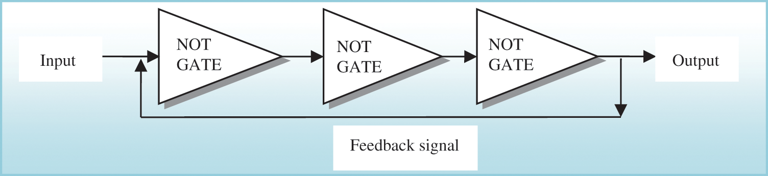
Figure 1: Three stage single ended ring oscillator
By using odd numbers of inverters, the circuit cannot have fixed operating point. As a result the output should be oscillating in nature with satisfying the gain of a close loop system (larger than 1); the initial standard is met. Toward the second standard (achieve a phase shift of 180°), minimum 3-holdup cell are requisite [5,6]. The propagation delay is shown in the Fig. 2. The fastest oscillation can be achieved by three inverter stages. It is identified; the number of stages will enhance the power expenditure, so the planned RO is calculatingly planned by least delay stages. Fractional positive feedback is also recommended to diminish the power consumption. For the fundamental principle of three stage RO, let us assume the first NOT gate output is achieved by time t1 voltage switch to logic “1”. As soon as, logic “1” propagates to the closing stage, it produces logic “1” to the third stage. This is again feedback to the input and generates logic “0” to the first inverter output. Once this logic “0”, propagated to the loop, it will toggle the output of the 1st stage. For each rotation, an up and down transition will take place. The delay time of each stage is calculated by high-to-low (tPHL) and low-to-high (tHPL) transitions [7]. Yet, both times are not equal as a result the average propagation delay (tPHL + tHPL)/2 can be valid. The whole oscillation period is calculated as T = 2ntd and frequency of oscillation is
To fulfill the Barkhausen’s criteria, the phase shift of total circuit is equal to 180°. Therefore, for this oscillator, all the stages must contribute 60° phase shift. The magnitude of gain @ oscillation frequency should be ≥ 1. Thus,
So the gain of every stage must be greater or equal to 2 (
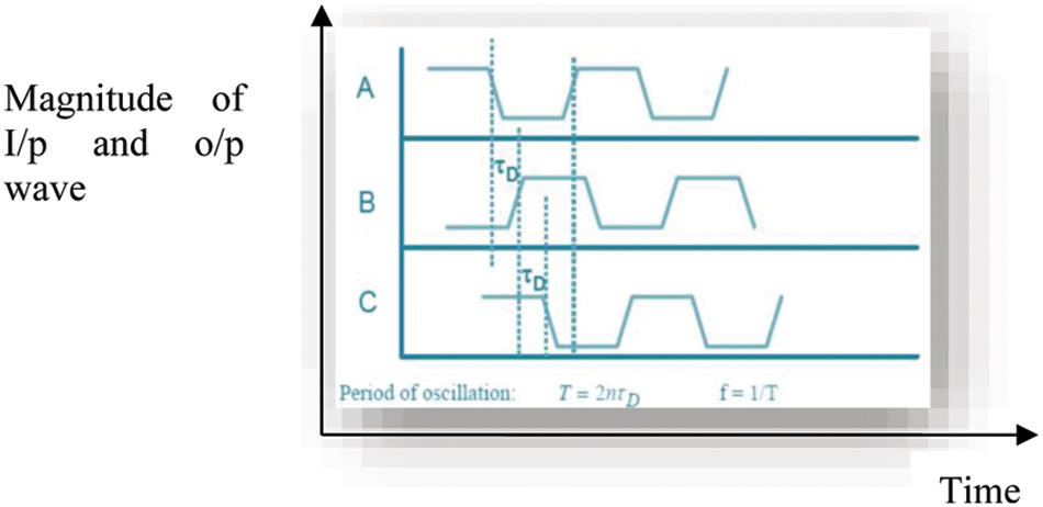
Figure 2: Output response of ring oscillator
As describe by the Fig. 2 A, B and C are the clock, input and output waves are shown respectively. The delay of input and output throughput is shown. For all the inverter circuit the fan-out is one [9,10]. The main benefit of ring oscillator is the designing of circuit: with transistor designing, it uses very less area so the power density is very low. This oscillator is easy to tune so it provides wide bandwidth. The major problem with this oscillator is poor phase noise. As a result, this is mainly used for clock recovery, generation, and synchronization. As odd numbers of inverter stages are used to the circuit it do not have constant quiescent point so it and oscillate [11]. The primary motive for CMOS oscillator is to use for high frequencies, low power expenditure plus superior phase noise rather than other VCO designs. The fine-tuning of ring oscillator is lying on the supply voltage as well as the length of transistor’s channel. Conversely, the supply effect is less as compared to the channel width and length of transistor, however the realistic constraints limits these parameter to an optimum range [12]. In the Section 2, the basic delay cell is discussed with switched diagram. Section 3, represents the performance of ring oscillator with fixed capacitor. In Section 4, the variable sweep capacitor is used with ring oscillator and simulation consequences are presented. In Section 5, the result analysis is discussed and in the Section 6, the conclusion is made based on circuit analysis.
CMOS based inverter circuit is used as delay cell to form the ring oscillator. The odd numbers of inverters are connected in series to provide oscillations to the circuit. For the designing of ring oscillator, three conjugative stages are used for the proposed design.
Fig. 3 shows a ring oscillator inverter cell. This is using two transistors (PMOS and NMOS) in a cascaded manner. When the input is high, it will provide the low output and vice versa. For 45 nm, CMOS technology the charge carrier mobility of NMOS is 2.5 times of PMOS mobility. So aspect ratio of 2.66 is selected for PMOS and NMOS [13,14] transistors.
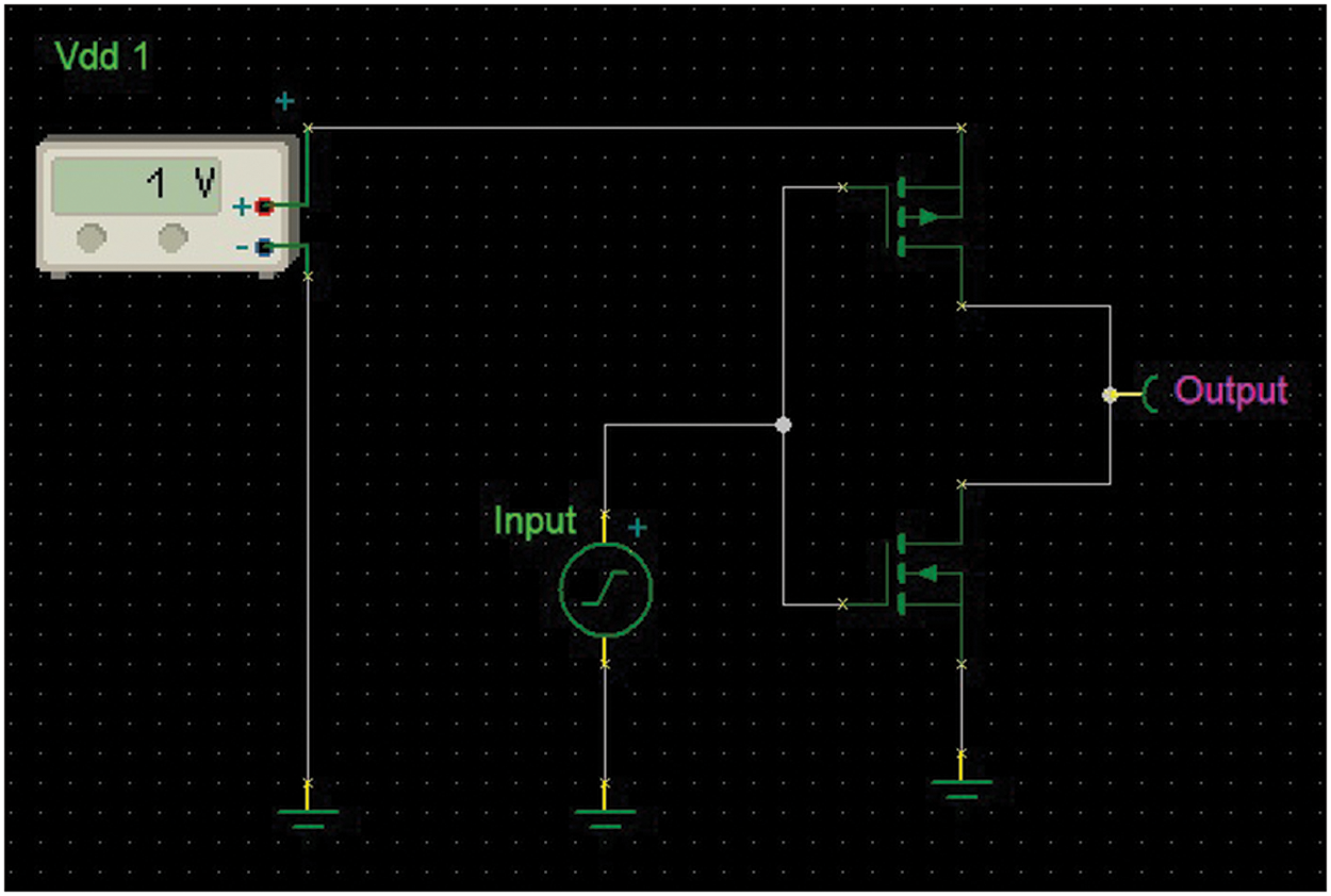
Figure 3: CMOS implementation of NOT gate (delay cell)
The Fig. 4 shows the input and output waveforms of CMOS inverter. The propagation delay of inverter is dependent on the time constant of the projected circuit. The time constant is dependent on the pull down resistor and the load capacitor values [15]. The schematic diagram of inverter with load capacitor is shown in Fig. 5. The switch analysis is subjected by the capacitance connected at the output (CL) that is tranquil of diffusion capacitances (Drain) of NMOS and PMOS transistors, wire capacitances plus i/p capacitance of gates connected at load (Eq. (6)). Let us assume, for low to high changeover, the PMOS is working as static switch. The response time of gate is the time; take to charge CL via PMOS internal resistance Rp. So the propagation delay (tpLH) of the circuit is proportional to the time constant RpCL [16]. Therefore, a rapid gate is built; whichever via choosing the low output capacitance or else through decrease the PMOS resistance.
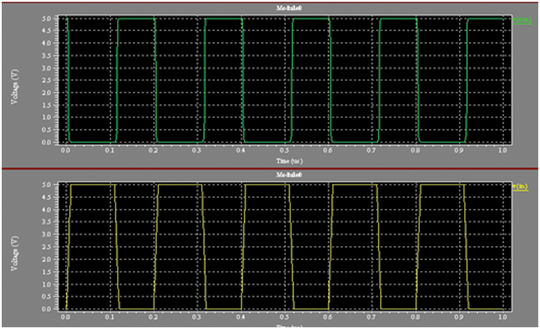
Figure 4: Simulated I/P and O/P waveforms of inverter

Figure 5: The switched diagram of inverter with load capacitor
The second one can be achieved via increasing the W/L (Aspect Ratio) of the transistor. The analogous conditions are applicable for high to low transition time delay (tPHL), dominated by RnCL. As the turn on resistance of both transistors are not constant, although having a nonlinear role of voltage applied across the transistor. This complicates the precise calculation of overall propagation delay. So by taking the average of high to low and low to high transition we get,
where: Wn is the width of the p transistors and Wn is the width of n type transistor, Ln & Lp are the length of n type and p type transistor, Cox is capacitor density of gate oxide (25 fF/ μm2), Kn & Kp are the trans-conductance of p type and n type transistor, Rn & Rp is the internal resistance of n type and p type transistor, VT is threshold voltage (-0.22 V for PMOS and 0.22 V for NMOS) [17]. In view of the fact that every facet positioned to the pathway, create some leakage value of resistance to the ground, and this will reduces the overall gain of the system. By escalating the feedback path resistor, its outcome can also be minimized and the oscillating frequency is minimized, as they are inversely proportional to each other [18]. This type of arrangement is only worn for rapidity modeling. Furthermore, to fulfill the Barkhausen criteria some amount of noise is also needed. Intrinsic amount of noise is amplified to the high gain and provides sustained oscillations. In view of the fact, that the power utilization is subsequently important for designing of any oscillator. The configuration of ring oscillator consists of a source with the same gain stages to produce periodic waveforms by a set frequency [19]. The frequency is controlled by adjusting the delay of the gain stage. This is capable by varying the available current toward the charging of the load capacitor of the circuit. The overall power debauchery can be separated in two parts. The first one is the power consumed by the current source and another is by the overall circuit. The totality of power dissipation is PTotal = VDD Ic = VDD (n CLVc f0). At the similar time, power degenerate by the inverters is P = Vc Ic = N CLVc2f0 .The dissipated power (Pcs) by current source is Pcs = PTotal-P = VDD (N CLVc f0)–N CLVc2f0. Where, Vc is average energy across the inverter, Ic is the current flowing through the load capacitor, fo is the frequency of oscillation of the circuit. For low power systems, it is essential to diminish power expenditure [20,21]. The overall power expenditure is related to number of stages used to the circuit and the related load capacitor. By minimizing the voltage across capacitor, the power loss by the inverter cell is also reduced. In addition, this will result to diminish the phase noise of the circuit. A midway has to be finding for good performance of the circuit.
3 Three Stage Oscillator with Fixed Capacitor
This circuit is having three inverter positioned in cascading. An uncomplicated three-stage ring oscillator is shown in Fig. 6. As high digital signal is applying to the input of first inverter, it propagates to the cell and low signal is delivered to the output. Again, this signal is fed back towards the input terminal and again this succession is started. As for the inverter circuit, as low signal is apply to the inverter input, the PMOS is turned on and NMOS is turned off so it will produce high signal at output. This high signal is fed to the next stage input terminal. This will switch off the PMOS and switch on the NMOS, consequently produce a low signal [22,23]. For suitable operation of ring oscillator, it requires odd numbers of NOT gates. The oscillating frequency can be calculated by the following equation Eq. (8).
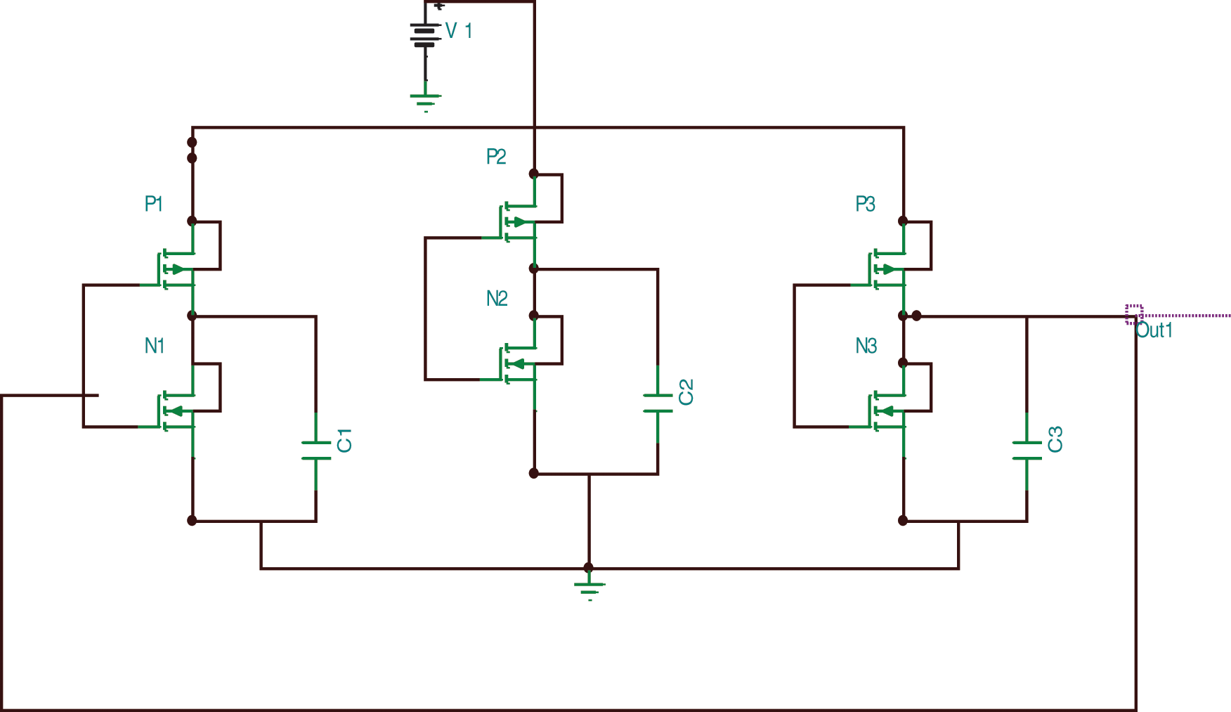
Figure 6: Simulated model of cmos based ring oscillator with 45 nm technology
The oscillation frequency is the inverse of the output time of a signal to process via an inverter cell. It is calculated by the estimation of rise time and fall time of the considered signal. For the oscillator triggering an initial voltage is applied to the circuit. Supply of 1 V is used at this point to generate the output to the circuit. The supply voltage is always greater to the threshold voltage Vth. Just the once, ring oscillator is triggered; it will continuously oscillated until the running point is up [22]. The applied capacitors range will affects the charging and discharging time. For this simulation, 1 pF capacitor is used. This external load capacitor is quite large to the gate capacitor (in femto-farad) for both NMOS and PMOS device. Fig. 7 shows the output response of the simulated oscillator.
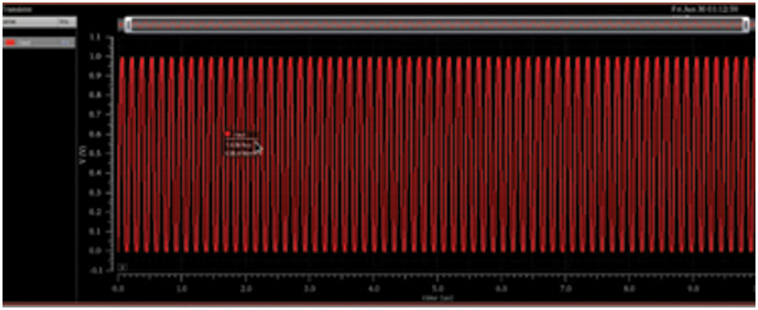
Figure 7: Output waveform of 45 nm ring oscillator (VCO)
For designing of 3-stage ring oscillator, first the delay cell is designed for 45 nm CMOS technology. For delay cell: The length of PMOS and NMOS (Lp = Ln) is 45 nm. When the voltage transfer curve intersect the unity gain line, defined as Vout = Vin. The device transconductance (β), of NMOS is βn = kn (Wn/Ln) and for PMOS βp = kp (Wp/Lp). The ratio of
The running time of ring oscillator circuit is 200 ns. In favor of initial performance validation, this time is stretched enough so that the values can be straightforwardly deliberated. Although, this step time is excessively huge so the output waveform may be abrupt or imprecise. A step time of 10 ns was used to generate smooth output waveform.
4 Simulations and Analysis of Ring Oscillator with Sweep Capacitor
The circuit diagram Fig. 8 of three-stage ring oscillator is used with the variable capacitor. The variable capacitor is used to find out the frequency analysis based on the different parameters. The circuit diagram of three variable capacitor ranges from 1 to 100 pF is shown to the figure. As by the output waveforms, it is shown that as the value of capacitor is low the circuit produces the high frequency.
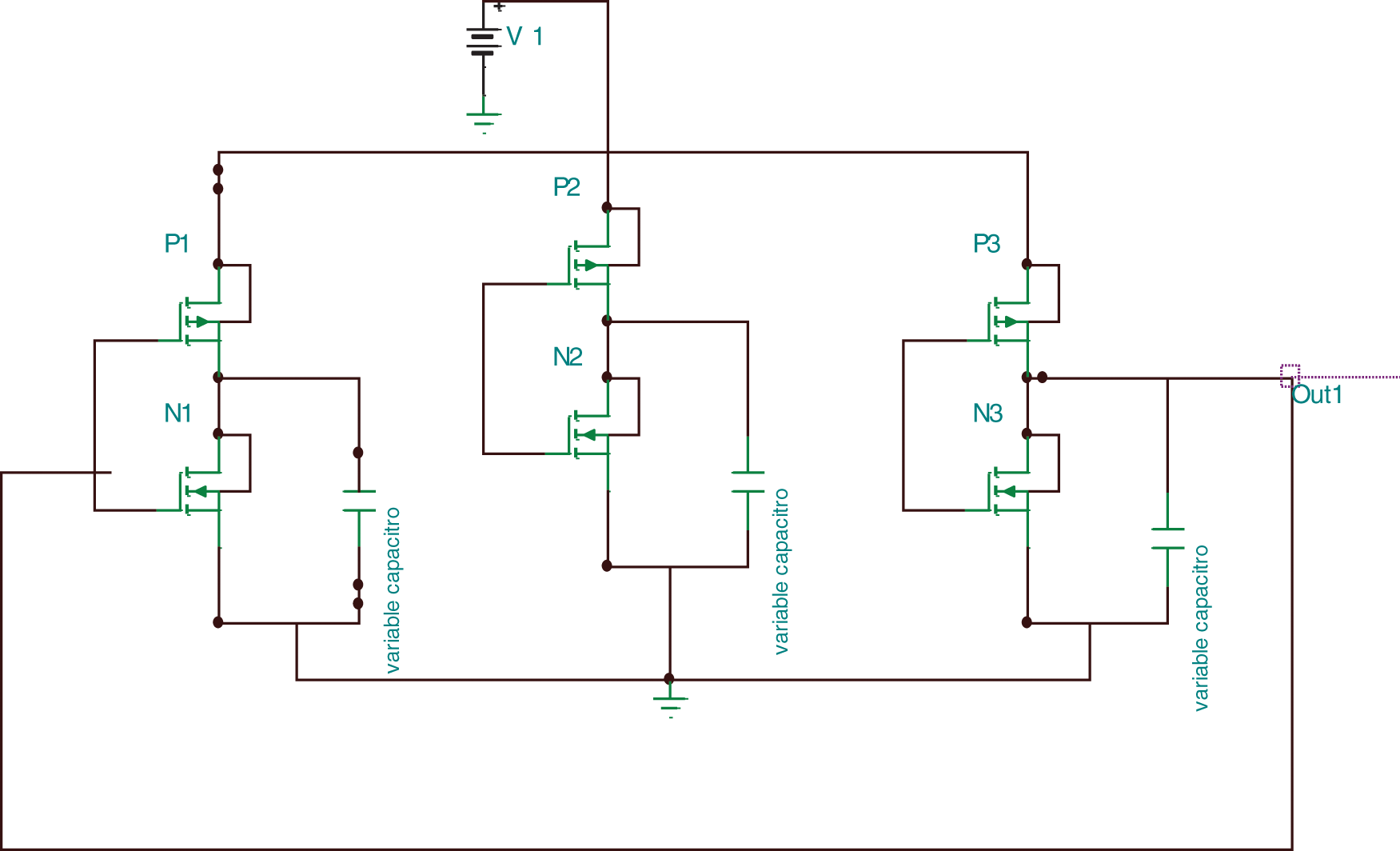
Figure 8: Simulated circuit diagram using variable capacitor
The overall simulated output waveforms with variable capacitance values are shown by the following Figs. 9 to 11.
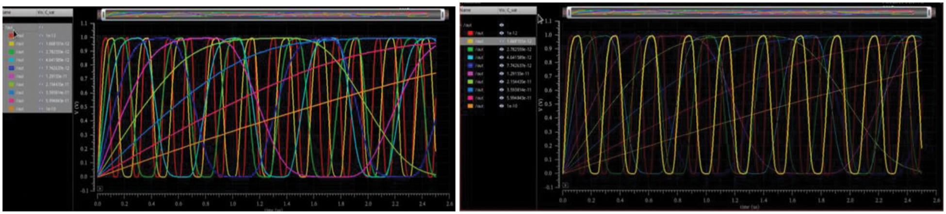
Figure 9: The O/P waveforms @1 pF to 100 pF capacitors values
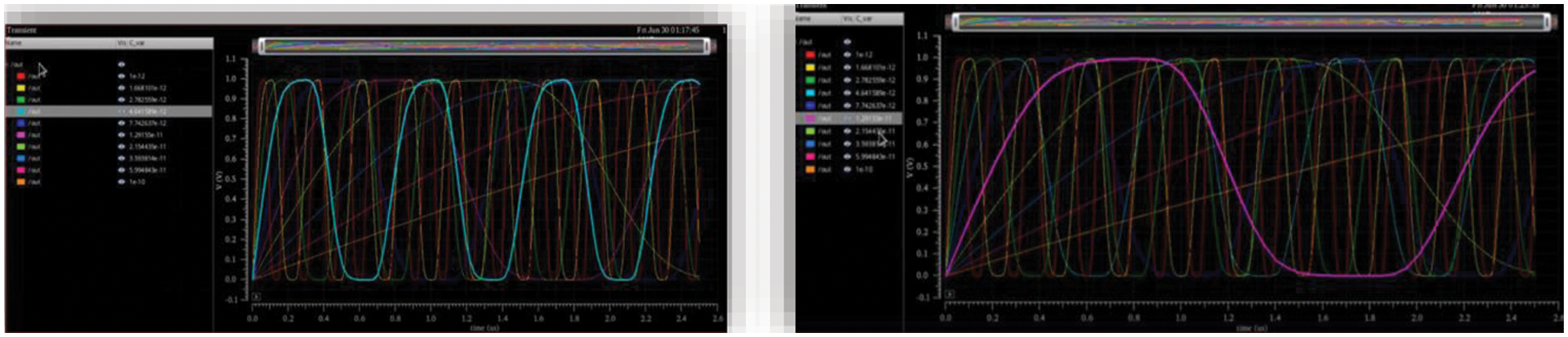
Figure 10: Output responses @ 1.668 pF and @ 2.78 pF capacitor
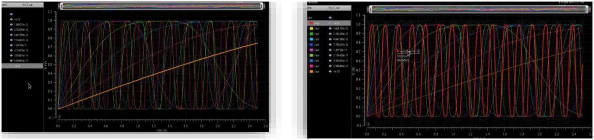
Figure 11: Response @ 4.64 pF capacitor and @ 1 to 100 pF capacitor
The different parameter obtained by the frequency analysis and the output responses are presented by the Tabs. 2 and 3. The different values of capacitor will alter the values of frequency obtained. As by the result, it is clear that by increasing the capacitor value the obtained frequency is low. Therefore, both the parameters are inversely proportional. The Figs. 12 and 13 are the pictorial graphs of the relation of both the parameters.
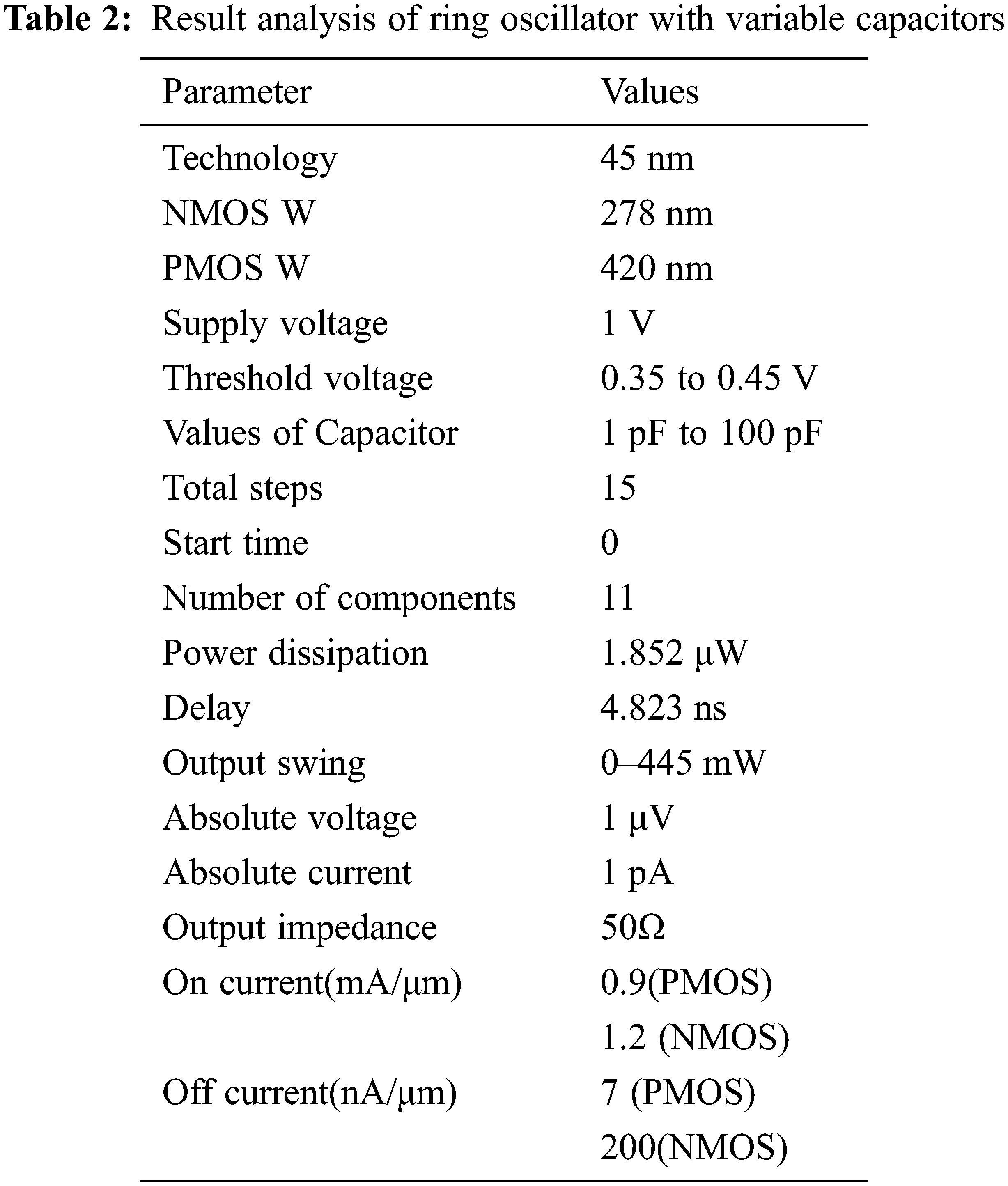
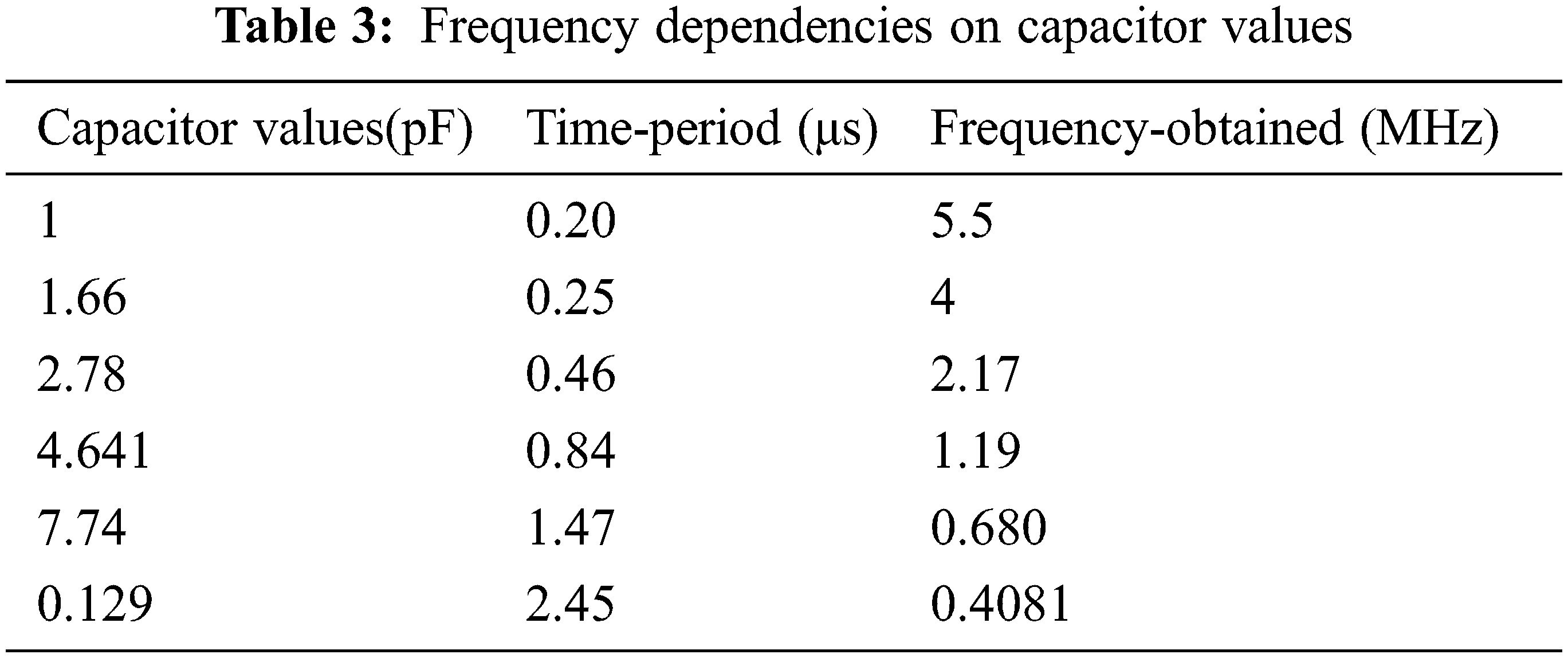
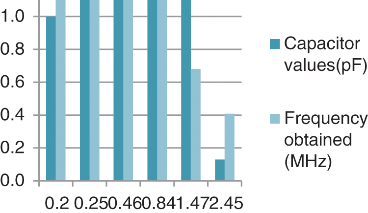
Figure 12: Bar chart of obtained frequency and variable capacitor
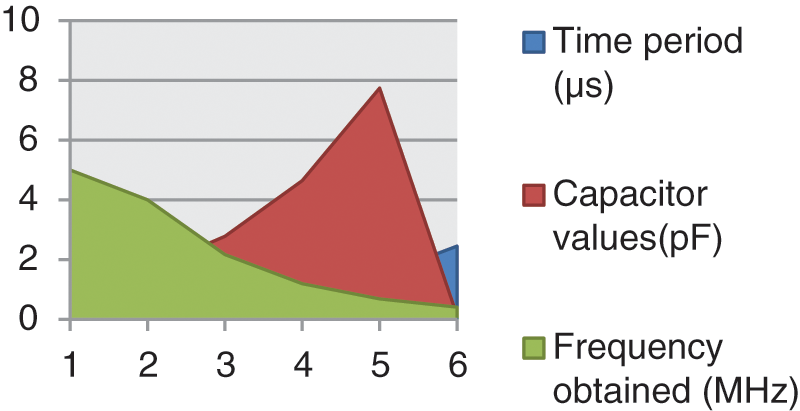
Figure 13: Area diagram of time period and frequency of ring oscillator
The graph shows the relation between capacitor value and the value of frequency.
The 5 MHz frequency band has unsurprising propagation merits that unite the paramount aspect for 40 meters and 80 meters range. This can be used to provide stable NVIS interactions throughout dusk and shadows. The operational frequency is based on the main parameters like time period and the capacitor values. In the core work, a 45 nm CMOS transistor is designed and simulated using cadence tool. The main ring oscillator is designed using 1 pF fixed capacitor and having 5.2 MHz frequency with Threshold voltage of −0.22 V and 0.22 V. The oscillations are smooth without glitch. The striking feature for this paper is taken a tradeoff among capacitor and frequency values. In this paper various performance curve for the relation of frequency and capacitor values is established. The projected ring oscillators attain the frequency range of 0.4081 to 5.2 MHz with the variable capacitance for three-stage ring oscillator. The power consumption of 1.852 μW is analyzed at 1 V supply for three-stage oscillator. This oscillator is used for CW mode radio communication, high part transmitters, clock generation, data transfer systems and recovery systems, and low power applications.
Funding Statement: The authors received no specific funding for this study.
Conflicts of Interest: The authors declare that they have no conflicts of interest to report regarding the present study.
References
1. J. F. Parker and D. Ray, “A 1.6-GHz CMOS PLL with on-chip loop filter,” IEEE Journal of Solid-State Circuits, vol. 33, no. 33, pp. 337–343, 1988. [Google Scholar]
2. P. K. Hanumolu, “Analysis of charge-pump phase-locked loops,” IEEE Transactions on Circuits and Systems-I: Regular Papers, vol. 51, no. 9, pp. 1665–1674, 2004. [Google Scholar]
3. D. Harikrushna, M. Tiwari, J. K. Singh and A. Khare, “Design, implementation and characterization of XOR phase detector for DPLL in 45 nm CMOS technology,” Advanced Computing: An International Journal, vol. 2, no. 6, pp. 45–57, 2011. [Google Scholar]
4. U. Kumari and R. Yadav, “Design and implementation of digital phase lock loop: A review,” International Journal of Advanced Research in Electronics and Communication Engineering, vol. 7, no. 3, pp. 197–201, 2018. [Google Scholar]
5. L. Kyoohyun, “A Low-noise phase-locked loop design by loop bandwidth optimization,” IEEE Journal of Solid-State Circuits, vol. 35, no. 6, pp. 807–815, 2000. [Google Scholar]
6. W. Abbas, Z. Mehmood and M. Seo, “A V-band phase-locked loop with a novel phase-frequency detector in 65 nm CMOS,” Electronics, vol. 9, no. 1502, pp. 1–12, 2020. [Google Scholar]
7. N. D. Patel and A. P. Naik, “A low jitter–low phase noise wideband digital phase locked loop in nanometre CMOS technology,” International Journal of Electronics and Communication Engineering and Technology, vol. 9, no. 3, pp. 1–12, 2018. [Google Scholar]
8. D. A. Ramey, “A 2–1600-MHz CMOS clock recovery PLL with low-capability,” Analog Integrated Circuits and Signal Processing Journal, vol. 19, pp. 91–112, 1997. [Google Scholar]
9. D. Ghai and N. Jain, “All-digital phase locked loop (ADPLL)-A review,” International Journal of Electronics and Computer Science Engineering, vol. 2, no. 1, pp. 94–101, 2012. [Google Scholar]
10. P. Kumar and R. Yadav, “Design of CMOS based FM quadrature demodulator using 45 nm technology,” International Journal of Research and Science Engineering, vol. 3, no. 7, pp. 12–16, 2016. [Google Scholar]
11. L. Bitla, V. Saraswathi and H. M. Akano, “Analysis of NAND gate based phase frequency detector for phase locked loop,” Journal of Critical Reviews, vol. 7, no. 9, pp. 172–176, 2020. [Google Scholar]
12. S. Hathwalia and N. Grover, “A comparative study of ring VCO & LC-VCO based PLL,” International Journal of Engineering Research and Applications, vol. 9, no. 2, pp. 52–54, 2019. [Google Scholar]
13. B. Razavi, Design of Analog CMOS Integrated Circuits, 2nd ed., Boston, MA: McGraw-Hill, pp. 484–510, 2001. [Google Scholar]
14. K. Parmar, “All digital phase locked loop design for different applications: A review,” International Journal of Innovative Research in Technology, vol. 1, no. 8, pp. 96–99, 2014. [Google Scholar]
15. S. N. Dandare and A. H. Deshmukh, “Design of DPLL using sub-micron 45 nm CMOS technology and implementation using microwind 3.1 software,” Journal of Science and Technology, vol. 3, no. 1, pp. 22–32, 2018. [Google Scholar]
16. M. K. Mandal and B. C. Sarkar, “Ring oscillator: Characteristics and applications,” International Journal of Pure and Applied Physics, vol. 48, pp. 136–145, 2010. [Google Scholar]
17. L. M. A. Gonzalez, V. Medina, V. Kampus, S. Paton, L. Hernandez et al., “Ring-oscillator with multiple transconductors for linear analog-to-digital conversion,” Electronics, vol. 10, no. 1048, pp. 2–15, 2021. [Google Scholar]
18. T. B. Chan, P. Gupta, A. B. Kahng and L. Lai, “Synthesis and analysis of design-dependent ring oscillator (DDRO) performance monitors,” IEEE Transactions on Very Large Scale Integration (VLSI) Systems, vol. 22, no. 10, pp. 2117–2130, 2014. [Google Scholar]
19. M. Kumar, “VCO design using NAND gate for low power application,” Journal of Semiconductor Technology and Science, vol. 16, no. 5, pp. 650–656, 2016. [Google Scholar]
20. S. R. Balaji, Y. Shivananda, N. L. Kumar, H. B. Ravindra and C. Ram, “Design and performance analysis of low frequency CMOS ring oscillator using 90 nm technology,” in IEEE Int. Conf. on Recent Trends in Electronics Information Communication Technology, India, pp. 1796–1801, 2016. [Google Scholar]
21. S. K. Gunda, R. S. E. Ravindran, B. Hemalatha and C. Divya, “Design and simulation of digitally controlled oscillator of ADPLL,” International Journal of Advanced Scientific Technologies in Engineering and Management Sciences, vol. 5, no. 3, pp. 1–4, 2019. [Google Scholar]
22. H. B. Ravisaheb and B. H. Nagpara, “2.4 gbps clock and data recovery using CMOS 45 nm technology,” International Journal of Advance Research in Engineering, Science & Technology, vol. 4, no. 3, pp. 383–389, 2017. [Google Scholar]
23. M. Esmaeilzadeh, Y. Audet, M. Ali and M. Sawan, “A very low-phase-noise CMOS ring VCO intended for sensor interfaces,” IEEE Transaction on Circuit and Systems—I: Regular Papers, vol. 1, pp. 1–9, http://doi.org/10.36227/techrxiv.14067713.v1 2021. [Google Scholar]
Cite This Article
 Copyright © 2023 The Author(s). Published by Tech Science Press.
This work is licensed under a Creative Commons Attribution 4.0 International License , which permits unrestricted use, distribution, and reproduction in any medium, provided the original work is properly cited.
 Downloads
 Citation Tools