
 Submit a Paper
 Propose a Special lssue
 Open Access
ARTICLE
Design and Analysis of Cascaded Hybrid-Bridge Multi-Cell Multilevel Inverter with Reduced Total Harmonic Distortion Profile
1
Lovely Professional University, Jalandhar, 144402, India
2
College of Engineering and Technology, Bhubaneswar, 751003, India
* Corresponding Author: Bulbul Sharma. Email:
Energy Engineering 2022, 119(6), 2585-2605. https://doi.org/10.32604/ee.2022.021465
Received 16 January 2022; Accepted 23 April 2022; Issue published 14 September 2022
 View Full Text
 Download PDF
Abstract
This multilevel inverter methodology is the center of focus among researchers in recent era. It has been focused due to its advantages over existing topologies, drawbacks and improvement of power quality, Multi-level inverter has the ability to generate nearly sinusoidal waves. This sinusoidal wave can be further improved by increasing the level of output voltage or with the help of filter design, and this manuscript presents single-phase Multi cell Multi-Level Inverter (MLI). It has been considered for reducing component count to get a higher number of output voltage levels and lower Total harmonics distortion profile. It comprises with four symmetric DC input voltage and 10 IGBT switches to produces stepped output of 9 level, and when deploy asymmetric Dc voltage source the same circuit will produce 31 level output with some changes in firing scheme, moreover this circuit is the family of cascaded hybrid bridge inverter so this circuit covered advantage of CHB MLI, This circuit uses lower no. of switch as compared to existing conventional MLIs such as FC-MLI, CHB-MLI, NPC-MLI, This paper also provides one of most pertinent controls and modulation mechanisms for a MLI using a hybrid reference/carrier-oriented sinusoidal PWM mechanism. At last, simulated outcomes are to validate the performance of both architectures in MLI structure as well as verify the concept.Keywords
MLI has been increasingly noticed in current decades due to their capacity to operate at high voltages, with maximum ease, and with minimal electromagnetic interference (EMI) [1]. MLI has no IGBT; this IGBT has different stress voltage, conduction, and switch times [2]. The multi-level inverter has the lowest total harmonic profile [3] without in type of filter [4]. The quality of a multi-level inverter can be enhanced by increasing its number of output voltage levels [5]; however, this process increases number of power switches [6], which leads to an increase in its cost & system complexity [7], so researchers are focusing on decreasing its number of switch count and increasing its output levels [8].
Popular MLI are categorized into two main categories: one of them, whose shared single Dc voltage source, like diodes clamped MLIs (DC-MLI) [9] & flying capacitors MLIs (FC-MLI) [10], and another one, isolating Dc voltage source [11], like cascade, as mentioned in Fig. 1. Newest MLI family and architectures at which Dc Input voltage remain the same here in [12]. The MLI is an appropriate option for significant power ratings, good quality output waveforms, and decent dynamic performance [13].
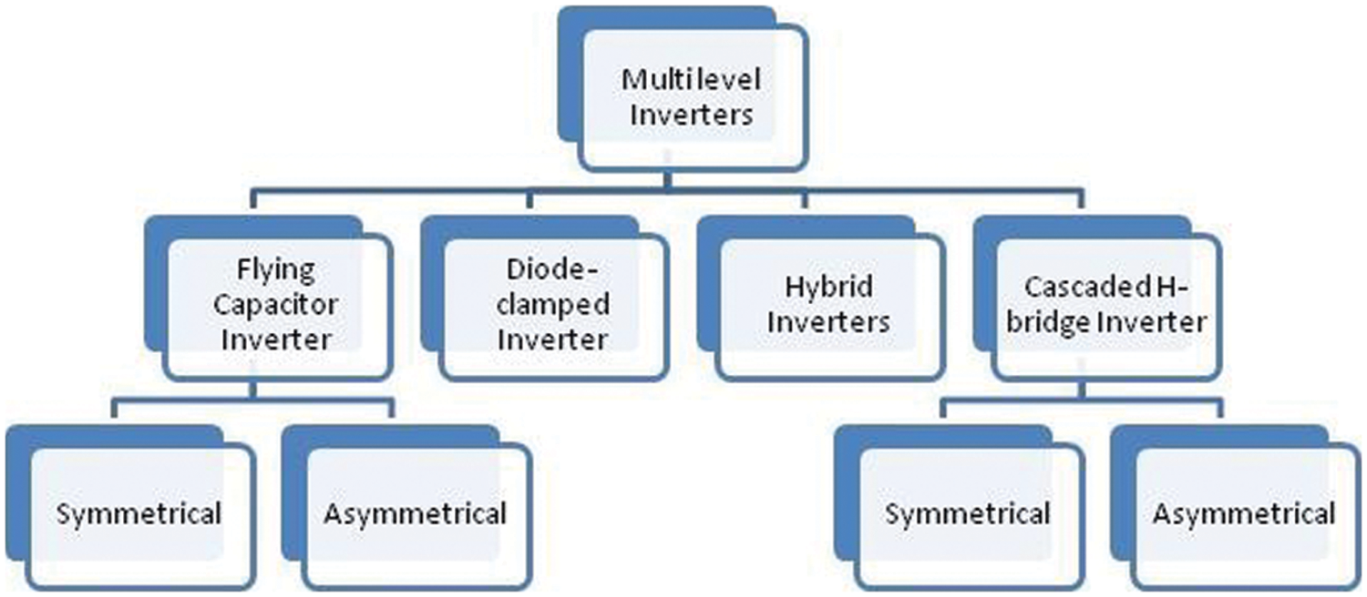
Figure 1: Types of multilevel inverters [10]
The drawback is MLI requires a higher number of power switching devices to produce output [14], and due to a higher number of devices, we need higher firing gate pulses to synthesize the output voltage [15]. As a result, the entire system could become more costly and complicated [16].
Among all such topologies [17], the cascaded hybrid bridge inverter [18] also has the most popular topology [19]; this inverter topology continues to focus on research due to its simplicity of expansion to the appropriate number of levels [20]. Cascaded MLIs have been built by connecting multiple 1-phase inverters in sequence; the above architecture may achieve moderate output voltages [21]. In determining the magnitude of the Dc voltages employed [22], cascaded hybrids bridge MLIs [23] may also be broken into two classes based on Dc source amplitude [24]. If the entire Dc voltages source has the same magnitude [25], then MLI is said to be symmetrical; otherwise, it is considered asymmetrical [26]. The adaptability of an asymmetrical cascaded hybrid bridge inverter [27] is appropriate for achieving a higher number of levels, although it typically needs a higher semiconductor device [28]. The modularity of symmetric Cascaded H-Bridge (CHB) MLIs is reasonable, but it uses many semiconductor devices [29]. As a result, asymmetric cascaded Hybrid Bridge MLIs [30] is used to obtain a high voltage level for a given switch [31]. And here, we discussed the CHB family’s topology with the implementation of Symmetric and asymmetric methodology [32] and a smaller number of power devices compared to the existing MLI topology [33]. This new topology can achieve 31 levels with asymmetric Dc voltage, and when deploying a symmetric Dc voltage source [34], the same circuit will produce nine-level voltage output; here, we define controllability [35], methodology, & THD (Total Harmonic Distortion) [36] profile with the help of MATLAB simulation.
As we have seen in Fig. 2, modification of the basic main circuit to the modified circuit, the question is, what is the need for this type of modification required, as we have considered the multi-level inverter (MLI) base circuit for the modification and enhanced the performance [36].
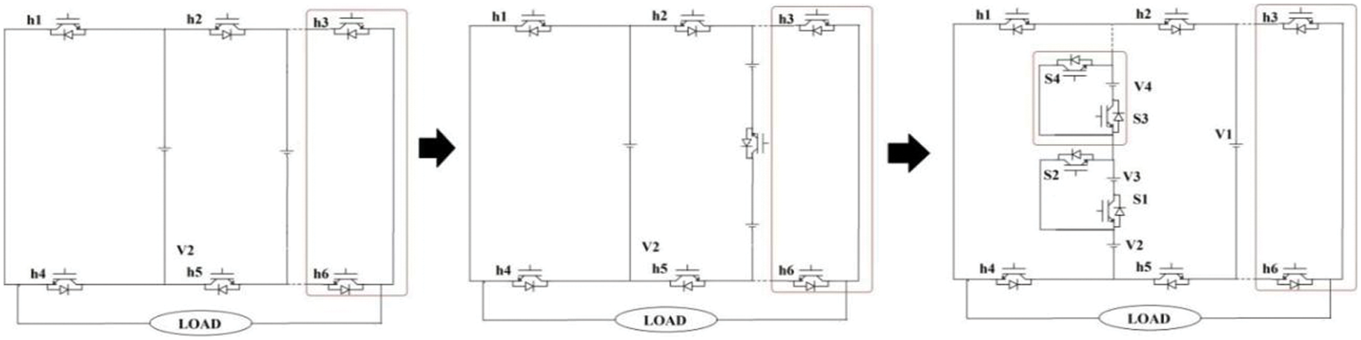
Figure 2: General single-phase circuit of MLI (a) Base circuit (b) Semi cross switched multi-level inverter (c) Semi-cascaded multilevel inverter
We observe that the Base circuit, modified with an additional IGBT and one Dc source [37], means the circuit’s output voltage increase one level [38], so the circuit output voltage waveform improved; next stage, the same circuit is modified with another Dc voltage source and IGBT’s [39], effectively increases no. of output voltage levels so the output of circuit would be improved [40].
Here are some reasons to move this multilevel inverter modification.
• We will not be able to get a MLI, as demonstrated in Fig. 2c without the development of circuit (b).
• In another one, we will not be able to use an asymmetric voltage source to achieve higher no. of levels with circuit (b), so it is mandatory part to modify another stage, as shown in Fig. 2c.
• Circuit (c) can be utilized to attain 31 levels of voltage output with the help of an asymmetric voltage source.
2.1 Generalized Structure of Semi-Cascaded MLI
The number of components needed in MLI topologies according to the input Dc voltage. It indicates that no. of levels increase as input DC voltage increases. The essential components in MLI configuration are semiconductor devices and accompanying simple drive circuits. As even the number of components rises, so the size and price of the multilevel inverter will also increase, and the complexity of the control system will increase. Fig. 3 depicts the structure of a Multi-Cell Multilevel Inverter.
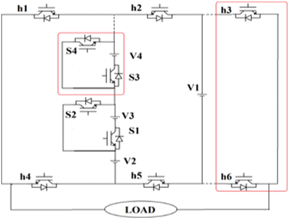
Figure 3: Semi-cascaded MLI
This circuit is implemented with the help of the symmetric Dc voltage supply, and when we use 4 symmetric voltage sources, it can achieve a 9-level of output and further increase its output level by increasing the number of cells or employing an asymmetric Dc voltage supply, it can achieve 31-level of output voltage with the same circuit by some modification in firing scheme, this is the one advantages of this circuit.
The presented circuit is motivated by preceding semi Cross Circuit switching Multi-level Inverters, as mentioned in Fig. 2b, and the appropriate linkage of many forms of cells with the help of 10 semiconductor devices that provide divergent routes to start generating the output voltage waveform within all phases with both positively and negatively polarization in output. Every cell is made up of semiconductor devices and one direct current source (Dc voltage source). It is also worth noting that V1 = Vdc inside the described architecture. Unique Dc sources voltage in each cell generates a given output voltage waveform. The offered inverters can supply the number of each Dc supply in the outputs. As a result, the highest voltage inside the outputs would equal the total of the amplitudes of the DC supply. Max output voltage (Vo, max) of architecture has represented by Eq. (1)
Wherever n = no. of Dc sources
Each switching causes an unwanted drop of voltage, which seems referred to as power losses in the form of switching and conduction loss. Switching loss occurs when the switch moves from an OFF to an ON and conversely. Conduction loss will create over the duration of one state. To compute the maximal voltage output, however, the ON-mode power loss of switching is considered to be Vdc, therefore Eq. (2) assesses the maximal voltage output when everyone switching power loss is included.
For asymmetric topology
For symmetrical topology
The switch voltage ratings are a key issue in multilayer inverters. The overall peak inverse voltages (PIV) of the switch is determined using the Eq. (4) below.
Magnitude value of all Dc voltage sources is equivalent to Vdc for symmetric inverters. In considering the symmetric architecture, the switch associated with a single Dc supply, Fig. 3, depicts the symmetrical inverter provided. The possible max voltages and also the number of operating voltages (m) inside the intended symmetrical inverters are described in the subsequent formula.
The Dc power supplies of the different cells in the intended asymmetrical MLI are not equivalent. With the same cell count, asymmetrical inverters deliver more stages in the output current than in their symmetrical equivalent.
The DC voltage of the separated cell in Fig. 3 is determined as per a geometric sequence with a component of p in the asymmetrical scheme.
It belong from 1 to n, whenever there are 2
For n-Dc source, max. Voltage and no. of Voltage stages are as follows:
Wherever n = no. of Dc source
The inverter’s modulation schemes are critical since they are directly connected to the system’s total performance [41]. MLI has investigated many forms of modulation schemes [42]. It is utilized to manage the output voltage/current and to calculate MLI’s two key parameters, low switching & percentage of THD [43]. A modulating signal’s goal was to provide a stepwise waveform which is the closest estimate of the particular reference signal, including variations in amplitude level, frequencies, and a vital element, i.e., typically sine’s wave in steady-state [44]. The simple visual depiction of total modulation approaches is displayed in Fig. 4. Depending on the switch’s frequencies, the two main modulation methods used in Multi-cell multi-level inverters [45] are Fundamental carrier frequency & fast switching frequency [46]. The two basics fast switching frequencies are PWM and space vector modulations [47].
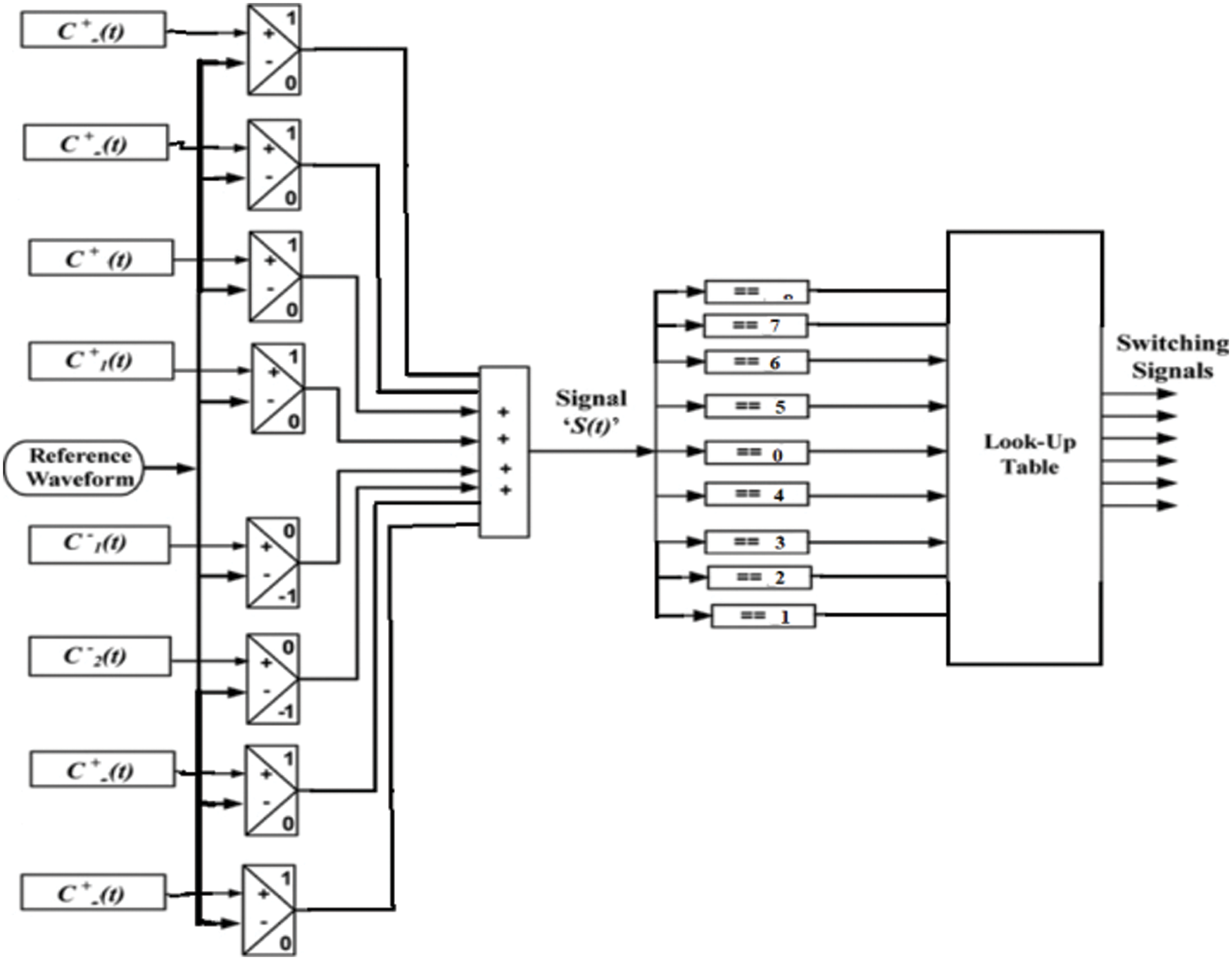
Figure 4: Multi-level inverter using a control scheme
In Multi-cell, Multi-level inverter modulator controls [48], high-switching-frequency modulation approaches such as the multi-carrier levels switch Pulse width modulation have been applied [49]. Low-switching-frequency approaches, on the other side, low-switching-frequency approaches include proactive harmonics removal [50], selective harmonic [51], and the Fundamental switching frequency technique [52]. This design may be changed using any one of these ways with appropriate adaption [53]. The multi-carrier PWM system is employed in this article. Inside a multi-carrier PWM system [54], the carrier’s signals are equated by the reference signals [55], & also the resulting waveforms are utilized to switch tools at different voltage levels [56]. In this design, one switch can assist in the synthesizing of many levels at the output terminals. Furthermore, as previously stated, appropriate usage of 10 modes (namely, modes 1, 2, 3…, & 10) would result in basic T2 and T2 switches that carry voltage stress of 2-Vdc each one as opposed to other switches that carry voltage stress of Vdc, respectively. As a result, in this part, a control method is provided where such a move is used to generate 9-level outputs. Nevertheless, the operation could be applied to high-level inverters.
The figure depicts the modulation scheme’s circuit illustration in the Fig. 4, and also the waveform is represented in Fig. 5. The four triangular waves with frequencies of 2.2 kilohertz each are employed for the carrier. Carrier’s signals [57] are typically arranged in alternating phases oppositional [58]. This reference signal is a sine waveform [59] with a frequency of 50 hertz, but it has been converted sine wave into a full-wave rectified signal because of ease of use, so half rectified signal finished at 0.01 another rectified signal has started after a phase shift of 0.01 and finished at 0.02, which is similar to the 50 hz frequency. Carrier signals [60] that are higher than the 0 reference value are denoted by way of “
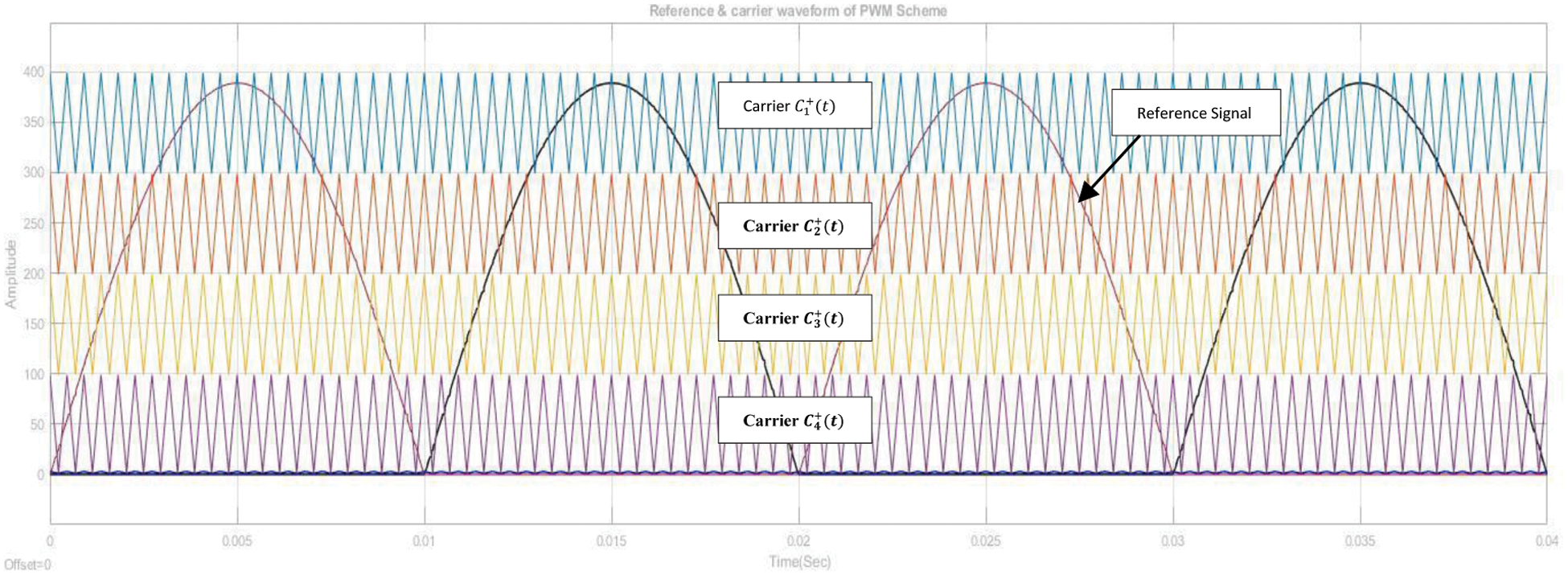
Figure 5: Reference waveform & carrier waveform for 9-level output scheme
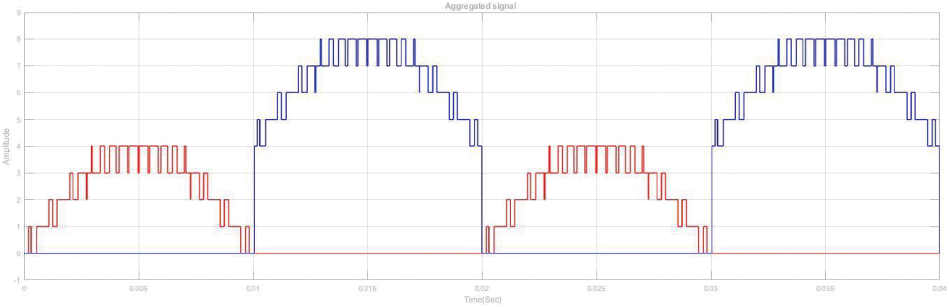
Figure 6: Aggregated signal
The MATLAB/Simulink tool is employed to make a MLI. 4 input Dc sources are employed, where E1 = 100 v, E2 = 100 v, E3 = 100 v, and E4 = 100 v as detail system specification mentioned in Table 1. The resulting switch pulses are displayed in Fig. 8, and their switch statistics are presented in Table 2 and Fig. 7; this reveals that switching h2 & h5 function at a core frequency of approximately 50 Hz, whereas switching h1, h4, h3, and h6 work at a freq. of 2.2 kHz. Therefore, lower-voltage-rated switches run at the higher frequencies, incurring switching loss, whereas higher-voltage-rated switches work at core frequencies, incurring a higher conductive loss. The net loss among the switching is allocated in this way.
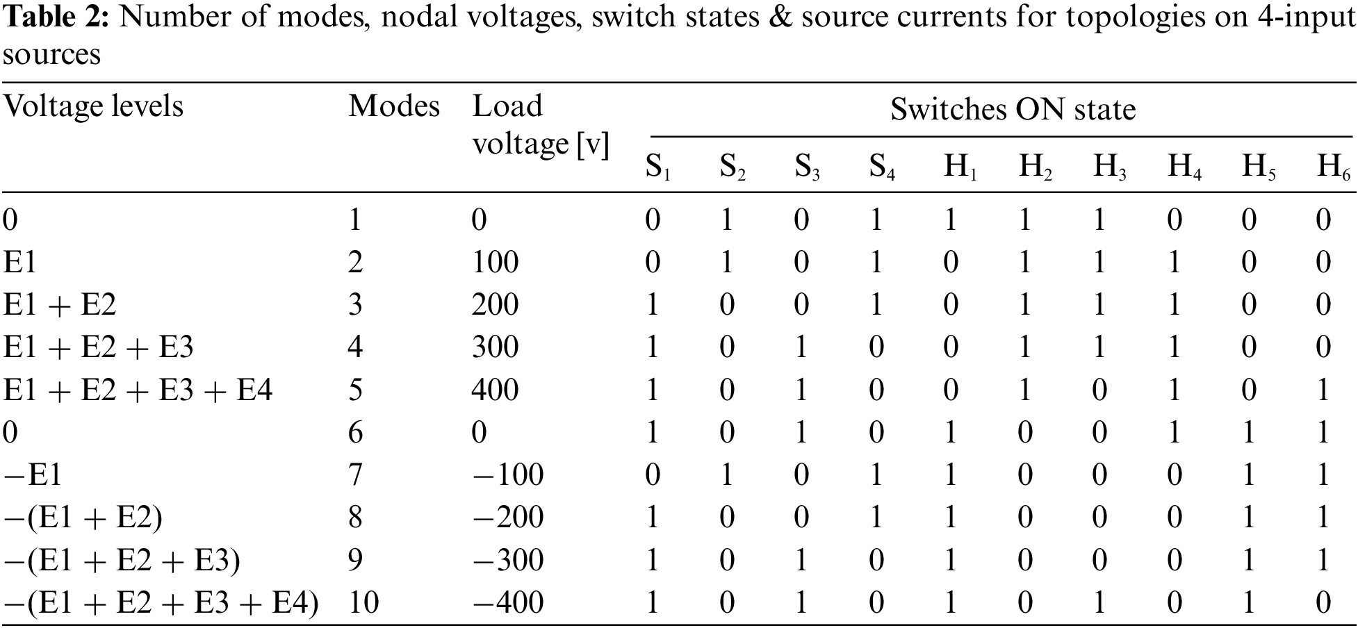
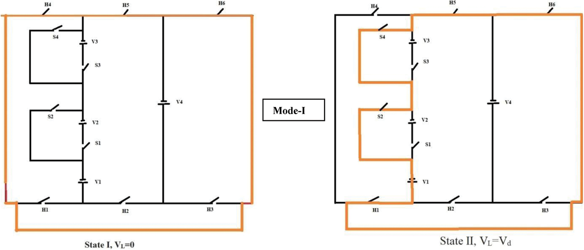
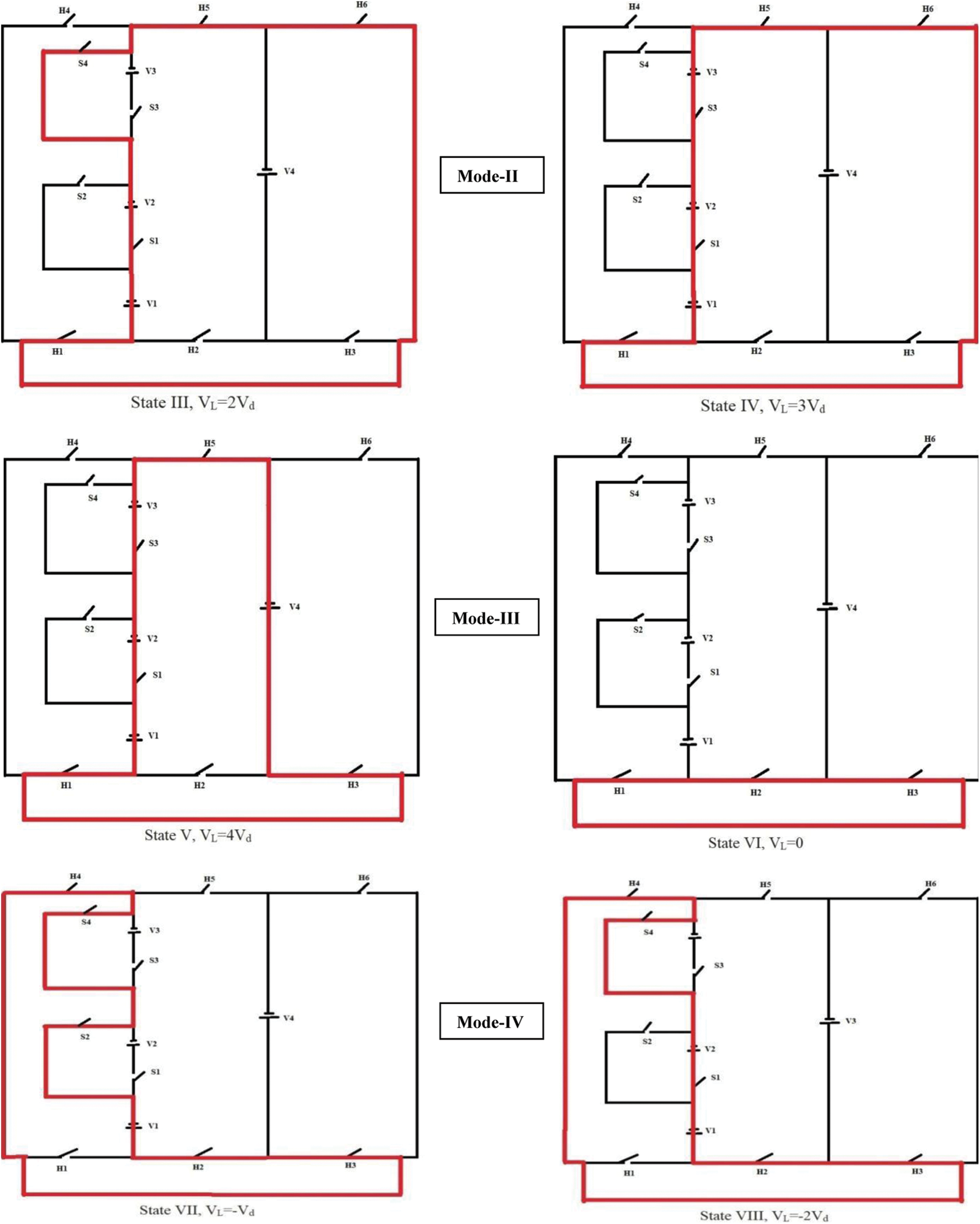
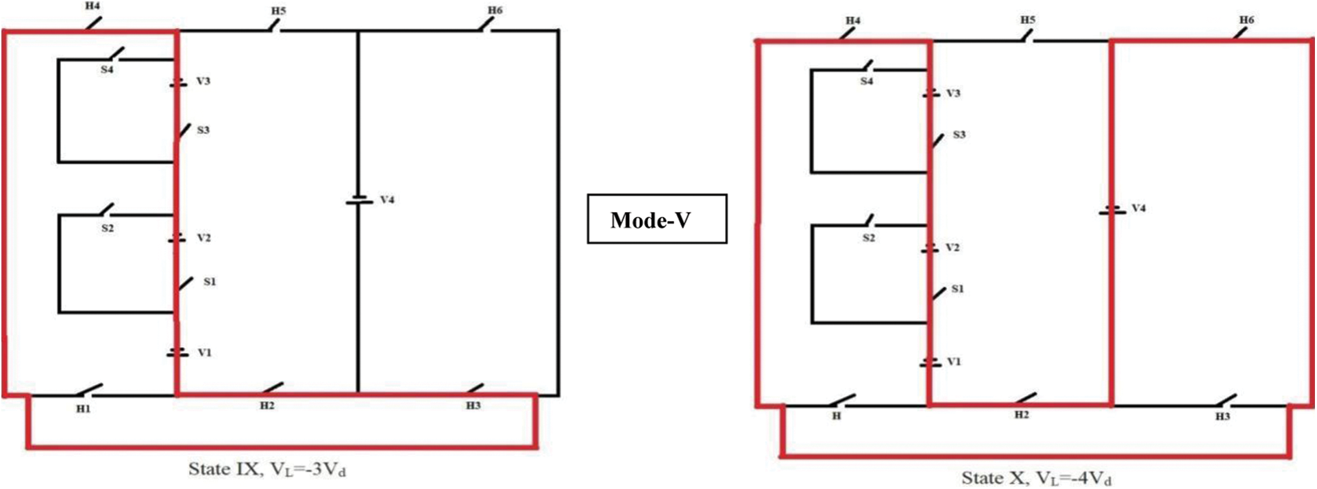
Figure 7: Multi-level working modes
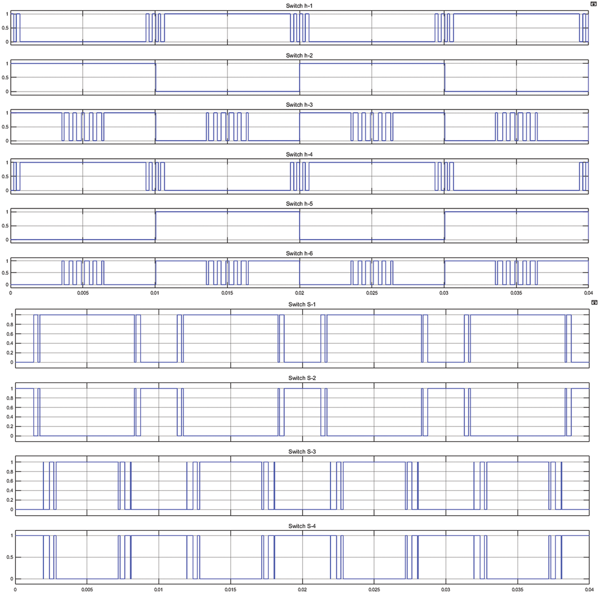
Figure 8: Gate switching pulses for the 9-level inverter
There are ten working states of the proposed circuit, by which got different nine levels, four different output produce positive half-wave another four sates produce a negative half-wave which as follows:
State I. To achieve voltage level (VL = ‘0’) on the connected load side, switches H4, H5, and H6 are switched ON. In this state, the total output voltage is zero at Load.
State II. To achieve a voltage level (VL = ‘+V1’ =100 v) on the connected load side, switches H1, S2, S4, H5, and H6 are switched ON. In this state, the total output voltage is 100 v at Load.
State III. To achieve a voltage level (VL = ‘V1 + V2’ =200 v) on the connected load side, switches H1, S1, S4, H5, and H6 are switched ON. In this state, the total output voltage is 200 v at Load.
State IV. To achieve a voltage level (VL = ‘+V1+ V2+ V3’ =300 v) on the connected load side, switches H1, S1, S3, H5, and H6 are switched ON. In this state, the total output voltage is 300 v at Load.
State V. To achieve a voltage level (VL = ‘V1 + V2 +V3+V4’ =400 v) on the connected load side, switches H1, S1, S3, H5, and H3 are switched ON. In this state, the total output voltage is 400 v at Load.
State VI. To achieve a voltage level (VL = ‘0’) on the connected load side, switches H1, H2 and H3 are switched ON. In this state, the total output voltage is 0 v at Load.
State VII. To achieve a voltage level (VL = ‘−V1’ = −100 v) on the connected load side, switches H3, H2, S2, S4, and H4 are switched ON. In this state, the total output voltage is −100 v at Load.
State VIII. To achieve a voltage level (VL= ‘−V1−V2 = −200’) on the connected load side, switches H3, H2, S1, S4, and H4 are switched ON. In this state, the total output voltage is −200 v at Load.
State IX. To achieve a voltage level (VL= “−V1−V2−V3” = −300) on the connected load side, switches H3, H2, S1, S3,& H4 are switched ON. In this state, the total output voltage is −300 v at Load.
State X. To achieve a voltage level (VL= ‘−V1−V2 −V3−V4= −400’) on connected load side, switches H6, H2, S1, S3, & H4 are switched ON. In this state, the total output voltage is −400 v at Load.
Figs. 9 and 11 illustrate the load voltage, current waveforms respectively Figs. 10 and 12 illustrate its harmonic spectra of load voltage and load current; results reveal that the 9-level reference voltage has equivalent stages at 100 volts each and a THD of 1.07 percent. Furthermore, given an R–L load, the load current waveforms (where R = 2 & L = 2 mH), then also its harmonics spectra, that is 0.14 percent.
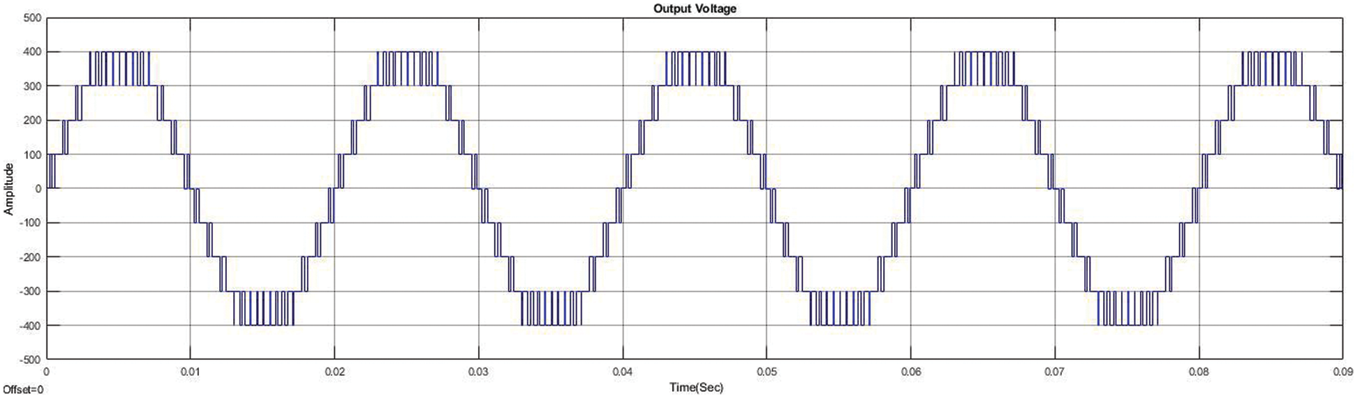
Figure 9: Simulation result of 9-level voltage output
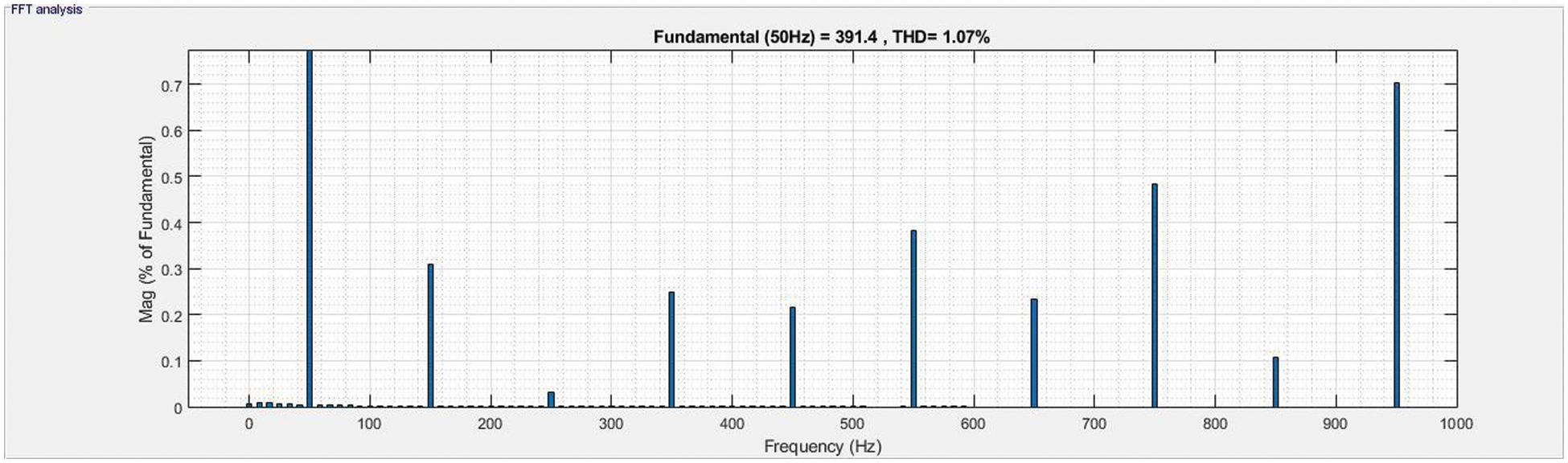
Figure 10: Total Harmonic distortion (THD) of output voltage
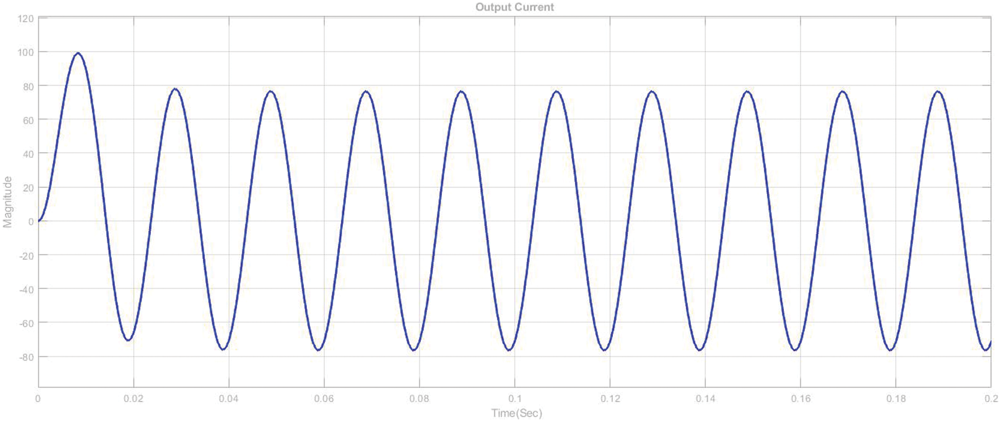
Figure 11: Simulating outcome of 9-level MLI current output
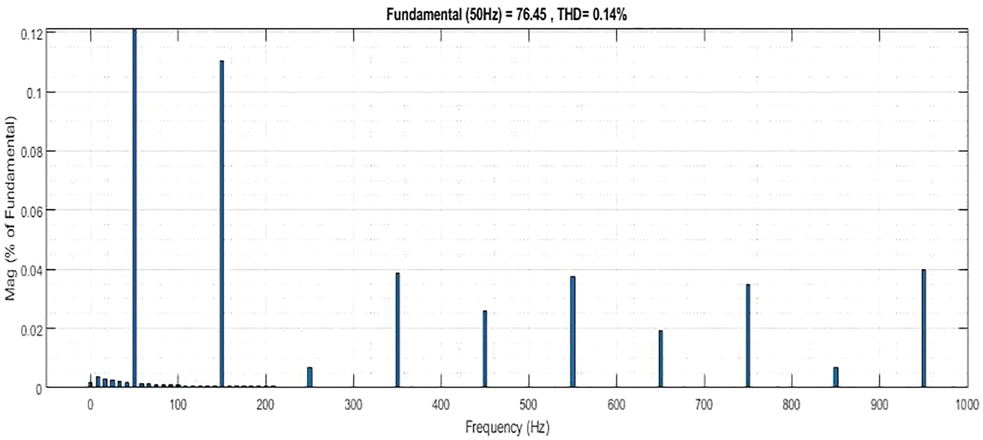
Figure 12: THD of output current
The related loss of voltage source converters is equivalent to the sum of energy losses caused by individual semiconductors. Loss sustained by a semiconductor diode is often classified into two types:
1. Whenever the circuit is in a block condition (that is, OFF-mode);
2. Whenever the circuit is in a conduct condition (that is, ON-mode).
While the circuit switches (that is, the changing mode from ON mode to OFF mode or conversely). Because leakage currents have been almost non-existent during block conditions [62], the loss remains small. As a result, just conduct & switch loss were taken into account when calculating loss related to these inverters.
As illustrated in Fig. 7, all switching needed in this architecture is unidirectional conduct & bidirectional block. The instant conduction loss of conventional transistors and diodes is.
Here,
VT & VD = ON-mode voltage drops.
RT & RD = equivalent ON-mode resistance of the transistors circuit & diodes, correspondingly.
α = constant governed by transistors features.
The conductive switch must carry the load current
To determine the overall switch loss, a standard switch is firstly analyzed, then separate power loss is therefore summed to give the overall switch loss of these inverters. For evaluating the isolated switch loss, current linear function & voltage linear function are utilized throughout the transient cycle (transit as OFF mode to ON mode & conversely). Power loss at start-up may be computed like
where, Eon,j = jth switch loss of turn-ON, ton = time for turn-ON, I = when switching upon that switch, electric current flows through all of it, Vo,j = voltage that must be blocked by the jth switch Likewise, the jth switch’s energy dissipation when turned off may be computed as
where
The jth switch performs fj changes in 1 s, wherein fj would be its carrier frequency. As a result, given I = I, the total switch power loss may be estimated as follows:
The next Section V (14) can be used to demonstrate that such a topology has reduced switch loss to the traditional CHB design. The overall inverter loss may now be calculated by Eqs. (11) and (14) as functions.
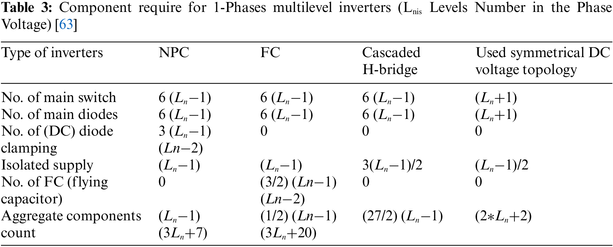
In this section, the presented topology has been compared in the manner of component requirement with the existing traditional topology such as NPC, CHB, and FC-MLI; as per the above discussion, seen that proposed MLI is the family of CHB multilevel inverter, proposed converter has four symmetrical input dc voltage, 10 IGBT switches producing stepped output with 1.07% THD without any type filter as shown in Figs. 10 and 12, in this category circuit has lowest THD profile with lower component count moreover level can be further increased by increasing number of cell or using asymmetrical DC voltage source. Table 3 shows a comparison of component needs for this proposed topology concerning the number of DC input sources for a single-phase 9-level arrangement. The table indicated that the number of components throughout this architecture is lower than that of other architecture, specifically for a greater level of voltage. Furthermore, the overall voltage load carried by the primary switches and diodes throughout this design is almost the same as conventional topologies.
As stated earlier, for elaborated symmetric dc voltage source utilized in 9-level multi-cell MLI trade-off must be made among no. of power switch & standing voltage on power switches. Also, it has been presented that the number of switches = 10 can be agreat choice when it balances the counting of power switches & standing voltage on switches. Thus, experimental & simulation results are stated for the condition in which the number of switches n = 10. It is considered that two sub-multi cells are connected to each other. Consequently, the output of symmetric MLI depends upon the presented optimal device topology will be as demonstrated in Figs. 13a and 13b. This 9-level multi-cell MLI has four equal sources of DC voltage, leading to a 9-level multi-cell MLI. Amplitude of sources is E1 = E2 = E3 = E4 = 40 V & so peak of load voltage is 160 V. A series-connected (R–L) load with resistance & inductance of 82 mH & 60 is paired to output. 9-level MLI dependent upon presented topology (Figs. 13a and 13b) utilizes 10 power switch (IGBTs).
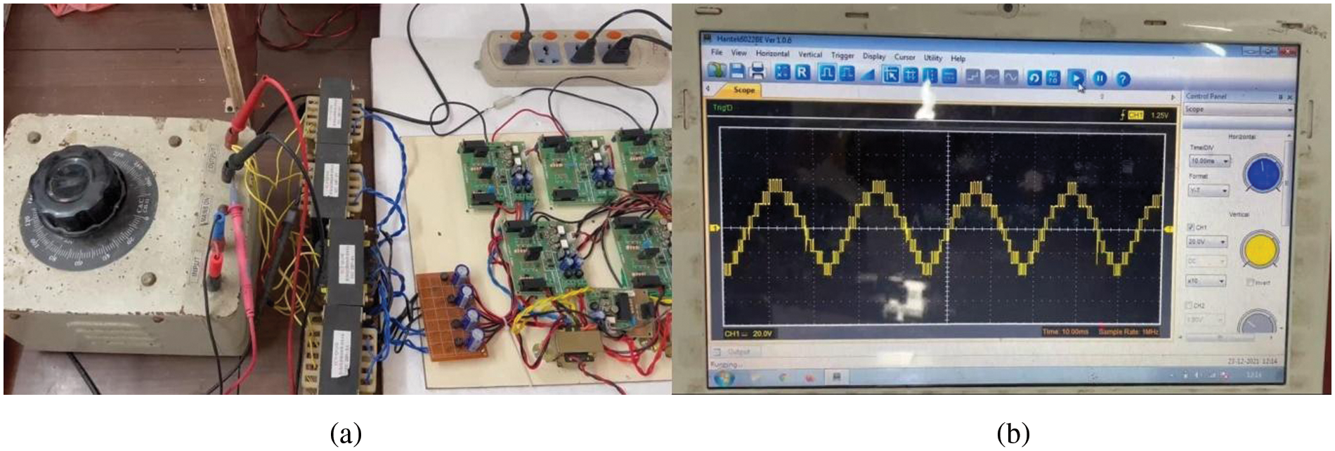
Figure 13: (a) Experimental setup (b) Experimental output voltage
In order to optimize the 9-level multi-cell, MLI staircase methodology is preferred. In this method, at any given point in time, the chosen level is the one closest to the reference output voltage. This process is also known as the nearest level approach. Using this technique, the output staircase voltage has the least inaccuracy concerning the reference voltage. Fig. 13a displays the prototype model. The prototype model has many circuits, each of which consists of IGBT power switch and a gate driver circuit for controlling the IGBT power switch gate. In addition to connection points for connecting the power circuit through wires and controller signals, the boards also provide connection points for the power circuit. Each board has its own power supply, which is used by a multi-tap-controlled power source. Also processed onboard are the rectifiers. In this design, MOSFET (IRF460) power switches (IGBTs) with internal anti-parallel diodes are employed. Each switch (GBT) is equipped with a gate driver circuit.
Gate firing signals of IGBT’s power switches are generated using the TMS320F28 Development kit. The microcontroller produced the gate firing pulses as per the table and connected it for gate driver topology, which drives power switches. As DC sources, the lab’s existing source voltage has been used. Figs. 13a and 13b depict the simulated and experimental output voltage findings, respectively. As indicated in the figures above, 9-level multicell MLI generates all anticipated voltage levels, resulting in a 9-level staircase output voltage. Output waveforms and their total harmonic profile seem to be in close accord with the getting of the corresponding simulations. The output AC load voltage is a stepped staircase waveform with levels of symmetrical magnitude. It’s also very important to note that power balance amongst input dc supplies is required with all dc sources to be having an equivalent lifespan. So, when dc sources, like PV cells, power rebalancing is especially critical.
This work presents a revolutionary architecture for MLIs to minimize the power switches and decrease their THD profiles. This topology’s operating principles have already been discussed, and mathematical formulas for o/p voltage and source current flow. This topology produces staircase results using different input DC voltage sources, which has the lowest THD profile, 1.07%, with a lower no. of switches count compared with the existing MLI topology; simulating experiments were carried out on a 9-level MLI with symmetrical DC voltage supply; when deploying asymmetric Dc voltage source, the same circuit will produce 31 level output with some changes in firing scheme. This topology is best to apply where a separate DC Supply is needed, such solar photovoltaic system. MATLAB Simulink was used to test this design.
Acknowledgement: I thank Dr. N. Karthick (EEE Department, LPU, Jalandhar, India) and Dr. D.P Bagarty (EE Department, CET, Bhubaneswar, India) for useful discussions. I thank the anonymous referees for their useful suggestions.
Funding Statement: The authors received no specific funding for this study.
Conflicts of Interest: The authors declare that they have no conflicts of interest to report regarding the present study.
References
1. Daher, S., Schmid, J., Antunes, F. L. M. (2008). Multilevel inverter topologies for stand-alone PV systems. IEEE Transactions on Industrial Electronics, 55(7), 2703–2712. DOI 10.1109/TIE.2008.922601. [Google Scholar] [CrossRef]
2. Sadigh, A. K., Hosseini, S. H., Sabahi, M., Gharehpetian, G. B. (2010). Double flying capacitor multi-cell converter with pulse width modulation that changes in phase. IEEE Transactions on Power Electronics Journal, 25(6), 1517–1526. DOI 10.1109/TPEL.2009.2039147. [Google Scholar] [CrossRef]
3. Banaei, M. R., Salary, E. (2011). Reduced the number of switches and the gate driver in a new multilevel inverter. Energy Conversion and Management, 52(2), 1129–1136. DOI 10.1016/j.enconman.2010.09.007. [Google Scholar] [CrossRef]
4. Solatialkaran, D., Gharani Khajeh, K., Zare, F. (2021). A novel filter design method for grid-tied inverters. IEEE Transactions on Power Electronics, 36(5), 5473–5485. [Google Scholar]
5. Babaei, E., Hosseini, S. H., Gharehpetian, G. B., Tarafdar Haque, M., Sabahi, M. (2007). Reduction of dc voltage sources and switches in asymmetrical multilevel converters using a novel topology. Electric Power Systems Research, 77(8), 1073–1085. DOI 10.1016/j.epsr.2006.09.012. [Google Scholar] [CrossRef]
6. Sivakumar, K., Das, A., Ramchand, R., Patel, C. (2010). A hybrid multilevel inverter topology for an open-end winding induction motor drive using two-level inverters in series with a capacitor-fed H-bridge cell. IEEE Transactions on Industrial Electronics, 57(11), 3707–3714. DOI 10.1109/TIE.2010.2040565. [Google Scholar] [CrossRef]
7. Rodriguez, J., Lai, J., Peng, F. Z. (2002). Multilevel inverters: A survey of topologies, controls and applications. IEEE Transactions on Industrial Electronics, 49(4), 724–738. DOI 10.1109/TIE.2002.801052. [Google Scholar] [CrossRef]
8. Rodriguez, J., Bernet, S., Steimer, P., Lizama, I. (2010). A survey on neutral point-clamped inverters. IEEE Transactions on Industrial Electronics, 57(7), 2219–2230. DOI 10.1109/TIE.2009.2032430. [Google Scholar] [CrossRef]
9. Dargahi, V., Sadigh, A. K., Abarzadeh, M., Pahlavani, M. R. A., Shoulaie, A. (2012). Flying capacitors reduction in an improved double flying capacitor multi-cell converter controlled by a modified modulation method. IEEE Transactions on Industrial Electronics, 27(9), 3875–3887. [Google Scholar]
10. Chen, A., He, X. (2006). Research on hybrid-clamped multilevel-inverter topologies. IEEE Transactions on Industrial Electronics, 53(6), 1898–1907. DOI 10.1109/TIE.2006.885154. [Google Scholar] [CrossRef]
11. Tolbert, L. M., Habetler, T. G. (1999). Novel multilevel inverter carrier-based PWM methods. IEEE Transactions on Industry Applications, 35(5), 1098–1107. DOI 10.1109/28.793371. [Google Scholar] [CrossRef]
12. Rodriguez, J., Bernet, S., Wu, B., Pontt, J. O., Kouro, S. (2007). Multilevel voltage-source-converter topologies for industrial medium-voltage drives. IEEE Transactions on Industrial Electronics, 54(6), 2930–2945. DOI 10.1109/TIE.2007.907044. [Google Scholar] [CrossRef]
13. Franquelo, L. G., Rodriguez, J., Leon, J. I., Kouro, S., Portillo, R. et al. (2018). The age of multilevel converters arrives. IEEE Industrial Electronics Magazine, 2(2), 28–39. DOI 10.1109/MIE.2008.923519. [Google Scholar] [CrossRef]
14. Zhiguo, P., Peng, F. Z. (2004). Harmonics optimization of the voltage Balancing control for multilevel converter/inverter systems. Proceedings IEEE 39th Annual Industry Applications Conference, vol. 4, pp. 2194–2201. Seattle, WA, USA. [Google Scholar]
15. Chiasson, J., Tolbert, L., McKenzie, K., Du, Z. (2003). Real-time computer control of a multilevel converter using the mathematical theory of resultants. Journal Mathematics and Computers in Simulation, 63(3–5), 197–208. DOI 10.1016/S0378-4754(03)00067-3. [Google Scholar] [CrossRef]
16. Banaei, M. R., JannatiOskuee, M. R., Kazemi, F. M. (2013). Series H-bridge with a stacked multi-cell inverter to quadruplicate voltage levels. IET Power Electronics, 6(5), 878–884. DOI 10.1049/iet-pel.2012.0667. [Google Scholar] [CrossRef]
17. Babaei, E., Hosseini, S. H. (2009). New cascaded multilevel inverter topology with a minimum number of switches. Energy Conversion and Management, 50(11), 2761–2767. DOI 10.1016/j.enconman.2009.06.032. [Google Scholar] [CrossRef]
18. Banaei, M. R., Salary, E. (2011). Verification of new family for cascade multilevel inverter switch reduction of components. Journal of Electrical Engineering and Technology, 6(2), 245–254. DOI 10.5370/JEET.2011.6.2.245. [Google Scholar] [CrossRef]
19. Kouro, S., Malinowski, M., Gopakumar, K., Pou, J., Franquelo, L. et al. (2010). Recent advances and industrial applications of multilevel converters. IEEE Transactions on Industrial Electronics, 57(8), 2553–2580. DOI 10.1109/TIE.2010.2049719. [Google Scholar] [CrossRef]
20. Buticchi, G., Lorenzani, E., Franceschini, G. (2013). A five-level single-phase grid-connected converter for renewable distributed systems. IEEE Transactions on Industrial Electronics, 60(3), 906–918. DOI 10.1109/TIE.2012.2189538. [Google Scholar] [CrossRef]
21. Rodriguez, J., Lai, J. S., Peng, F. Z. (2002). Multilevel inverters: A survey of topologies, controls applications. IEEE Transactions on Industrial Electronics, 49(4), 724–738. DOI 10.1109/TIE.2002.801052. [Google Scholar] [CrossRef]
22. De, S., Banerjee, D., Siva Kumar, K., Gopakumar, K., Ramchand, R. et al. (2011). Multilevel inverters for low-power applications. IET Power Electronics, 4(4), 384–392. DOI 10.1049/iet-pel.2010.0027. [Google Scholar] [CrossRef]
23. Malinowski, M., Gopakumar, K., Rodriguez, J., Pérez, M. A. (2010). A survey on cascaded multilevel inverters. IEEE Transactions on Industrial Electronics, 57(7), 2197–2206. DOI 10.1109/TIE.2009.2030767. [Google Scholar] [CrossRef]
24. Rodriguez, J., Bernet, S., Wu, B., Pontt, J. O., Kouro, S. (2007). Multilevel voltage-source-converter topologies for industrial medium-voltage drives. IEEE Transactions on Industrial Electronics, 54(6), 2930–2945. DOI 10.1109/TIE.2007.907044. [Google Scholar] [CrossRef]
25. Tolbert, L. M., Peng, F. Z. (2000). Multilevel converters as a utility interface for renewable energy systems. 2000 Power Engineering Society Summer Meeting, vol. 2, pp. 1271–1274. Como, Italy. [Google Scholar]
26. Ebrahimi, J., Babaei, E., Gharehpetian, G. B. (2012). A new multilevel converter topology with a reduced number of power electronic components. IEEE Transactions on Industrial Electronics, 59(2), 655–667. DOI 10.1109/TIE.2011.2151813. [Google Scholar] [CrossRef]
27. Hinago, Y., Koizumi, H. (2012). A switched-capacitor inverter using series/parallel conversion with inductive load. IEEE Transactions on Industrial Electronics, 59(2), 878–887. DOI 10.1109/TIE.2011.2158768. [Google Scholar] [CrossRef]
28. Park, S. J., Kang, F. S., Lee, M. H., Kim, C. U. (2003). A new single-phase five-level PWM inverter employing a deadbeat control scheme. IEEE Transactions on Industrial Electronics, 18(3), 831–843. [Google Scholar]
29. Najafi, E., Yatim, A. H. M. (2011). Design and implementation of a new multilevel inverter topology. IEEE Transactions on Industrial Electronics, 59(11), 4148–4154. DOI 10.1109/TIE.2011.2176691. [Google Scholar] [CrossRef]
30. Pereda, J., Dixon, J. (2011). High-frequency link: A solution for using only one DC source in asymmetric cascaded multilevel inverters. IEEE Transactions on Industrial Electronics, 58(9), 3884–3892. DOI 10.1109/TIE.2010.2103532. [Google Scholar] [CrossRef]
31. Lipo, T. A., Manjrekar, M. D. (1999). Hybrid topology for multilevel power conversion. US Patent: 6005 788. [Google Scholar]
32. Kou, X., Corzine, K. A., Familiant, Y. L. (2002). Full binary combination schema for floating voltage source multilevel inverters. IEEE Transactions on Industrial Electronics, 17(6), 891–897. [Google Scholar]
33. Ounejjar, Y., Al-Haddad, K., Dessaint, L. A. (2012). A novel six-band hysteresis control for the packed U cells seven-level converter: Experimental validation. IEEE Transactions on Industrial Electronics, 59(10), 3808–3816. DOI 10.1109/TIE.2011.2161059. [Google Scholar] [CrossRef]
34. Silva, C. A., Cordova, L. A., Lezana, P., Empringham, L. (2011). Implementation and control of a hybrid multilevel converter with floating DC links for current waveform improvement. IEEE Transactions on Industrial Electronics, 58(6), 2304–2312. DOI 10.1109/TIE.2010.2064277. [Google Scholar] [CrossRef]
35. Gupta, K. K., Jain, S. (2012). Topology for multilevel inverters to attain a maximum number of levels from given DC sources. IET Power Electronics, 5(4), 435–446. DOI 10.1049/iet-pel.2011.0178. [Google Scholar] [CrossRef]
36. Young, C. M., Chu, N. Y., Chen, L. R., Hsiao, Y. C., Li, C. Z. (2013). A single-phase multilevel inverter with battery balancing. IEEE Transactions on Industrial Electronics, 60(5), 1972–1978. DOI 10.1109/TIE.2012.2207656. [Google Scholar] [CrossRef]
37. Rohner, S., Bernet, S., Hiller, M., Sommer, R. (2010). Modulation, Losses, semiconductor requirements of modular multilevel converters. IEEE Transactions on Industrial Electronics, 57(8), 2633–2642. DOI 10.1109/TIE.2009.2031187. [Google Scholar] [CrossRef]
38. Ned, M., Undeland, T. M., Robbins, W. P. (2001). Power electronics: Converters, applications and design. 2nd edition. NJ, USA, Hoboken: Wiley. [Google Scholar]
39. Loh, P. C., Holmes, D. G., Lipo, T. A. (2005). Implementation and control of distributed PWM cascaded multilevel inverters with minimal harmonic distortion and common-mode voltage. IEEE Transactions on Industrial Electronics, 20(1), 90–99. [Google Scholar]
40. Yao, W., Hu, H., Lu, Z. (2008). Comparisons of space-vector modulation and carrier-based modulation of a multilevel inverter. IEEE Transactions on Industrial Electronics, 23(1), 45–51. [Google Scholar]
41. Du, Z., Tolbert, L. M., Chiasson, J. N. (2006). Active harmonic elimination for multilevel converters. IEEE Transactions on Power Electronics Journal, 21(2), 459–469. DOI 10.1109/TPEL.2005.869757. [Google Scholar] [CrossRef]
42. Chiasson, J. N., Tolbert, L. M., McKenzie, K. J., Du, Z. (2003). Control of a multilevel converter using resultant theory. IEEE Transactions on Control Systems Technology, 11(3), 345–354. DOI 10.1109/TCST.2003.810382. [Google Scholar] [CrossRef]
43. Blasko, V. (2007). A novel method for selective harmonic elimination in power electronic equipment. IEEE Transactions on Power Electronics journal, 22(1), 223–228. DOI 10.1109/TPEL.2006.886599. [Google Scholar] [CrossRef]
44. Angulo, M., Lezana, P., Kouro, S., Rodriguez, J., Wu, B. (2007). Level-shifted PWM for cascaded multilevel inverters with even power distribution. 2007 IEEE Power Electronics Specialists Conference, pp. 2373–2378. Orlando, FL, USA. [Google Scholar]
45. Galco. Galco Industrial Electronics. Inc. 26010 Pinehurst Drive, Madison Heights, MI, 48071. http://www.galco.com. [Google Scholar]
46. Carnielutti, F., Pinheiro, H., Rech, C. (2012). Generalized carrier-based modulation strategy for cascaded multilevel converters operating under fault conditions. IEEE Transactions on Industrial Electronics, 59(2), 679–689. DOI 10.1109/TIE.2011.2157289. [Google Scholar] [CrossRef]
47. Fracchia, M., Ghiara, T., Marchesoni, M., Mazzucchelli, M. (1992). Optimized modulation techniques or the generalized N-level converter. Proceedings IEEE Power Electronics Specialist Conference, pp. 1205– 1213. Madrid, Spain. [Google Scholar]
48. Corzine, K. A., Baker, J. R. (2002). Reduced parts count multilevel rectifiers. IEEE Transactions on Industrial Electronics, 49(3), 766–774. DOI 10.1109/TIE.2002.801077. [Google Scholar] [CrossRef]
49. Rao, S., Janiga, Varma, P., Srinivasa, Kumar, T. et al. (2018). Novel switching design structure for three-phase 21-level multilevel inverter fed BLDC drive application. International Journal of Power Electronics and Drive Systems, 9(3), 1202–1213. [Google Scholar]
50. Peng, F. Z. (2004). A generalized multilevel inverter topology with self-voltage balancing. IEEE Transactions on Industry Applications, 37(2), 611–618. DOI 10.1109/28.913728. [Google Scholar] [CrossRef]
51. Tummala, S. K., Dhasharatha, G. (2019). Artificial neural networks based SPWM technique for speed control of permanent magnet synchronous motor. E3S Web of Conferences, vol. 87, pp. 1–5. France, EDP Sciences. [Google Scholar]
52. Tummala, S. Kumar, Kosaraju, S. (2020). SEM analysis of grid elements in mono-crystalline and poly-crystalline based solar cell. Materials Today: Proceeding, vol. 26, pp. 3228--3233. [Google Scholar]
53. Rajagiri, A., Sandhya, M. N., Nawaz, S., Tummala, S. K. (2019). Speed control of DC motor using fuzzy logic controller by PCI, 6221 with MATLAB. E3S Web of Conferences, vol. 87, pp. 01004. France. [Google Scholar]
54. Kumar, T. S., Sankar, V. (2011). Reliability improvement of composite electric power system using unified power flow controller. IEEE India Conference, pp. 1--6. Hyderabad, India. [Google Scholar]
55. Bankupalli, P. T., Babu, V. S., Tummala, S. K. (2015). Modeling of static VAR compensator employing a cascaded H-Bridged multilevel converter. International Journal of Applied Engineering Research, 10(16), 37057–37062. [Google Scholar]
56. Reddy, B. Y., Rao, J. S., Tummala, S. K., Nagarjuna, A. (2019). Fifteen levels cross H bridge multilevel inverter fed PMSM. International Journal of Innovative Technology and Exploring Engineering, 8(11), 1194–1198. DOI 10.35940/ijitee. [Google Scholar] [CrossRef]
57. Ye, Z., Jain, P. K., Sen, P. C. (2007). Circulating current minimization in high-frequency AC power distribution architecture with multiple inverter modules operated in parallel. IEEE Transactions on Industrial Electronics, 54(5), 2673–2687. DOI 10.1109/TIE.2007.896143. [Google Scholar] [CrossRef]
58. Guerrero, J. M., Matas, J., de Vicuña, L. G., Castilla, M., Miret, J. (2006). Wireless-control strategy for parallel operation of distributed generation inverters. IEEE Transactions on Industrial Electronics, 53(5), 1461–1470. DOI 10.1109/TIE.2006.882015. [Google Scholar] [CrossRef]
59. Romero-Cadaval, E., Milanes-Montero, M. I., Gonzalez-Romera, E., Barrero-Gonzalez, F. (2009). Power injection system for grid-connected photovoltaic generation systems based on two collaborative voltage source inverters. IEEE Transactions on Industrial Electronics, 56(11), 4389–4398. DOI 10.1109/TIE.2008.2002734. [Google Scholar] [CrossRef]
60. Turner, R., Walton, S., Duke, R. (2010). Stability and bandwidth implications of digitally controlled grid-connected parallel inverters. IEEE Transactions on Industrial Electronics, 57(11), 3685–3694. DOI 10.1109/TIE.2010.2041741. [Google Scholar] [CrossRef]
61. Kadir, M. N. A., Mekhilef, S., Ping, H. W. (2010). Voltage vector control of a hybrid three-stage eighteen-level inverter by vector decomposition. IET Transactions. Power Electronics, 3(4), 601–611. DOI 10.1049/iet-pel.2009.0085. [Google Scholar] [CrossRef]
62. Rao, D. S., Rani, S. M. N., Nawaz, S. S., Tummala, S. K. (2019). Gate Driver Circuit Design, PWM signal generation using FEZ Panda III and Arduino for Inverter. E3S Web of Conferences, vol. 87, pp. 01003. EDP Sciences Database, France. [Google Scholar]
63. Lai, J. S., Peng, F. Z. (1996). Multilevel converters-A new breed of power converters. IEEE Transactions on Industry Applications, vol. 32, no. 3, pp. 509–517. [Google Scholar]
Cite This Article
 Copyright © 2022 The Author(s). Published by Tech Science Press.
This work is licensed under a Creative Commons Attribution 4.0 International License , which permits unrestricted use, distribution, and reproduction in any medium, provided the original work is properly cited.
 Downloads
 Citation Tools