
 Submit a Paper
 Propose a Special lssue
 Open Access
ARTICLE
Enhancement of Large Renewable Distributed Generation Penetration Levels at the Point of Common Coupling
Department of Electrical Power Engineering, Durban University of Technology, Durban, 4000, South Africa
* Corresponding Authors: Akinyemi Ayodeji Stephen. Email: ,
Energy Engineering 2022, 119(6), 2711-2744. https://doi.org/10.32604/ee.2022.023069
Received 07 April 2022; Accepted 18 June 2022; Issue published 14 September 2022
 View Full Text
 Download PDF
Abstract
The occurrence of distortion and over voltage at the Point of Common Coupling (PCC) of Renewable Distributed Generation (RDG) limits its penetration levels to the power system and the RDG integration is expected to play a crucial role in power system transformation. For its penetrations to be sustained without disconnection from the system, there must be a solution to the voltage rise, distortion, unbalanced current and grid reactive power control strategy at PCC. It is an IEEE-1547 requirement that RDG integration to the power system should be regulated at PCC to avoid disconnection from the network due to power quality criteria. RDG integration must meet up with this specification to uphold power quality and avoid damage to the sensitive equipment connected at PCC. In this paper, voltage rise, unbalanced current, reactive power and distortion are being managed at PCC while Distribution Network (DN) accepts more RDG penetration levels without violation of the IEEE and South Africa grid code act. Active Power Filter and Full Bridge Multi-Level Converter (FBMC) are considered to safeguard power quality to the grid, they are modelled in MATLAB/SIMULINK and the results obtained shown that the proposed strategy can successfully regulate voltage rise, distortion, unbalanced current and continuously improve power quality with RDG integration at PCC. The proposed method's key innovation is the strategic generation and absorption of reactive power to curtain an overvoltage, reverse power flow, and distortion at the PCC, allowing more RDG penetration levels to the grid without disconnection while maintaining the standard requirement for power quality at the PCC. The simulation outcomes validate the superiority of the FBMC over the active power filter with respect of reactive power generation/absorption, dynamic response, and damping capability.Graphic Abstract
Keywords
Nomenclature
| PSO | Power System Operator |
| PCC | Point of Common Coupling |
| RDG | Distributed Generation |
| IEEE | Institute of Electrical and Electronics Engineers |
| DN | Distribution Network |
| FBMC | Full Bridge Multi-Level Converter |
| IPP | Independent Power Producers |
| AC | Alternating Current |
| DC | Direct Current |
| Load Current | |
| Vector of Balanced Active Current | |
| Vector of Balanced Reactive Current | |
| Vector of the Unbalanced Current | |
| Vector of the Harmonic Currents | |
| A | Apparent Power |
| P | Active Power |
| Q | Reactive Power |
| D | Distortion |
| Load Distortion Factor | |
| Load Unbalance Factor | |
| Load Reactivity Factor | |
| Current Vector of the Compensation Network | |
| Current Vector of RDG | |
| Conductance of RDG | |
| Reference Signal | |
| Voltage at PCC | |
| Power Generated by RDG | |
| Unwanted Current Component | |
| Peak Value for Unwanted Component | |
| Scaling Coefficients | |
| Vector for Balanced Active Current | |
| Conformity Factors | |
| Power Factor | |
| Pre-set Reference Value | |
| Point of Common Coupling (PCC) voltage | |
| The Receiving end Power | |
| Voltage at the Load | |
| Resistance of the Line | |
| Reactance of the Line | |
| I | Current |
| Active Power Flowing through the Line | |
| Reactive Power Flowing through the Line | |
| Real Power Demand of the Load | |
| Reactive Power Demand of the Load | |
| S | Apparent Power |
| L | Inductance |
| R | Resistance |
| C | Capacitance |
| Z | Impedance |
All Loading capability and power reliability are some of the benefits of RDG integration to the power system, thereby permitting easy transferring of power to the grid. It is expected that power quality and voltage regulation should be adequately controlled and properly coordinated in such networks combining RDGs. A weak DN turns to active and smart network, the transformation occurs only by the connection of RDGs, incorporation of an automation system, communication, and information technology systems capable of monitoring power flows from points of generation to points of consumption. However, utility and Power System Operator’s (PSO) concern grow with the transformation of the RDG integration penetration levels and the challenges it brings to the system in respect of planning, safety, and control [1–3]. The power flows with DRGs connection are bidirectional unlike conventional with the unidirectional power flow, DRGs has altered the existing protection schemes, monitoring and method of control. DRGs integration to DN give a new approach to handle voltage rise regulation, distortion, voltage unbalance, and harmonics at the PCC without disconnection. These power quality issues are undeniably harmful to DNs, as evidenced by reduced cable life, deterioration of consumer electronics, and failure of variable speed drives [4]. Introduction of a robust control scheme at PCC, which can be existing in isolation to dampen the effects of voltage rise and distortion even when there are any grid disturbances, so that continuity of power supply would not be altered and would go a longer way. In such a situation, an algorithm-based decision should be considered to where reference signals would have been connected with the variabilities of the power quality criterion as established in the utility standard operation. Utility and Independent Power Producers (IPPs) experience lots of unbearable occurrences because of imbalance current from inductive loads, non-linear loads, unbalanced load and voltage rise at PCC. Overvoltage and reverse power flow at the point of interconnection is caused by the DG system supplying more real power than is required by the load, with the excess supplied back to the grid [5]. Power quality issue such as undervoltage, line losses, power factor correction etc., were being addressed in the past by the usage of capacitor banks [6,7]. Even at that, the occurrence of similar faults cannot be over-emphasised in power system because of the method in-effectiveness and also, some of the methods used cannot solved two or more power qualities problem at a time. For example, capacitor banks are used to solve power factor issue in the past, but it cannot solve voltage rise or distortions at PCC. Using palliative measure such as capacitor bank and passive filters to tackle some of these critical power quality challenges can result to more havoc than the initial condition [8,9]
It could be a bit difficult to compensate for voltage rise, unbalance voltage, harmonic, and power factor correction etc., with local means without the fore understanding of the design and load sequences involving the dynamic fluctuations in power system parameters at the PCC. Meanwhile, usage of active filtering circuitry was previously used [9], not because of the financial implication of the installation, but because of the extensive deployment of converters associated with RDGs integration to DN [10–12]. Power quality issues with renewable RDG systems are primarily caused by power electronic-based generation technologies rather than traditional synchronous generators, as well as the intermittent nature of RESs. The primary power quality concern is voltage and frequency fluctuations caused by uncontrollable inconsistency in renewable energy. The inconsistency of renewable energy behavior as a result of frequently changing weather characteristics causes voltage and frequency fluctuations at the grid of integration [13]. Modular multilevel converters were developed in response to the need for high-power converters with lower Harmonic distortion and higher efficiency. It was recommended to cut switching losses, strengthen output power quality, and distribute voltage evenly across switches [14]. FBMCs have emerged as attractive topologies for voltage applications, they offer scalable to high voltage without the need for series device connection, modular structure with internal fault management during operation and low semiconductor losses. Its modularity and functionality made it extremely adaptable to a wide range of applications. The converters produce a high-quality voltage waveform with a lower switching frequency, making them ideal for a variety of applications including high-power transmission in HVDC and renewable energy high-power motor drives such as railway traction motor drives and high-power accelerators. MMCs are now extensively used in both medium and high voltage transmission networks because they resolve most of those constraints of traditional VSCs, such as scalability to higher voltages through the addition of more levels, the requirement of smooth output voltage waveforms at a lower switching frequency, and the complete removal of low-order harmonics, which typically necessitate large filters [15,16]. The switching device blocking during a disturbance is appropriate to reduce any AC grid involvement in the DC fault current, which is one of the attractive characteristics of the device. Diverse features of the FBMCs have been researched, the basic operational principle, modulation and capacitor voltage balancing are presented in [17–19]. The authors in [20] implemented the application of a single reference per phase for sinusoidal pulse width modulation and staircase with the nearest voltage levels while fundamental switching frequency modulation and capacitor voltage balancing for multilevel converter is presented in [21]. The application of phase-shifted carrier pulse width modulation for multilevel converter, where each cell is controlled independently, including regulation of the cell capacitor voltages is considered in [22]. Hence, the assessment has not been made on the application capability of FBMC to mitigate distortion, unbalanced current and regulation of over voltage at the PCC. The RDGs integration gain attention because of their renewable sources, cleanness, flexibility, compliment to the energy supply by the utility, reduction in transmission losses, reduction in demand of energy from the utility companies and the resources is available and renewable on human time scale, etc. [23,24]. However, the power quality of these consumers needs to be reinforced for voltage rise, distortion, unbalanced current, extra consumption of reactive power and current harmonic at the PCC. This paper presents a method of regulating an over-voltage, unbalanced current and distortion at PCC with RDG Active Power Filter and Full Bridge Multi-Level Converter (FBMC) to safeguard power quality to the grid. The contribution of this research paper is as follows:
• The development of a techniques to control the potential threat of unbalanced current, and distortion at the PCC.
• The generation of positive reactive power during a worst-case scenario of a DN with RDG integration to control the phase angle and the reference point with FBMC.
• The proposed method generates high-quality AC and DC side waveforms with near-zero harmonics and DC ripples, attenuates voltage rise and reverse power flow, regulates active and reactive power, allowing more RDG penetration levels to the grid without disconnection while maintaining the PCC's standard power quality requirement.
2 Conventional Electrical Circuit Analysis
Consider the 3-
The voltage and the current should be regarded as unbalanced/distorted if a compensation is to be designed. Therefore, the connected converter’s reference signal at PCC can be obtained from Eq. (17) and the compensation should be considered for all the components of the current with respect to the load connected as expressed in Eq. (18). Based on the Eq. (18), each of the components or group is associated with the aim of the compensation, which means that the compensation strategy can be drawn. When RDGs are integrated into a distribution network, it is expected that energy is transported into the network, that is the aim. Therefore, there should be a way of generating a reference signal that will give way for power
The primary aim of compensation for power quality challenges at the PCC is to ascertain that the power quality absorbs or generated into the system is within an acceptable range establish by the utility or to international standard. Then the target aim is accomplished if some of the distortions at PCC are suppressed, unbalanced voltage made balanced, voltage rise mitigated, and harmonic reduced by the compensation strategy as compared to the initial state before the compensation. The fundamental rule of compensation can be expressed in Eq. (24), in this Eq. (24), the subscript
The vector to balance the active current in the network is regarded as
The reference signal signs would be convenient to obtain compensation in Eq. (44) haven got the pre-set values through Eqs. (25), (32), (34), (36), and (41)–(43). The power quality parameters will definitely remain within an acceptable range set by the unity and international standard. The expression in Eq. (45) can be referred to as a scaling factor. It is pertinent to know that if this Eq. (45) is equal to zero, then the maximum compensation can be achieved. However, if the Eq. (45) is equal to unity as expressed in Eq. (46), then it means that there is no application of compensation of the system. In a situation where there is no occurrence of power quality challenges in the network, that is to say that the system power factor is unity, hence, then the conformity factor in the equations in (32), (34) and (36) would be equal to zero.
The occurrence of over voltage at PCC creates an undue restriction to the integration of a large RDG to the power system. The current flowing across an electrical grid through resistance is directly proportional to the voltage at the PCC (Ohm’s law), such that the voltage increases with current or resistance. For AC system, the impedance is made of inductance, resistance, and capacitance, when these components are altered, the network power quality, voltage and current thereby improves or reduces. However, the reduction in the voltage due to the line impedance, the consumer loads connected to the system, the current that flows across and the sending end voltage determine the amount of receiving end voltage at the far end of the network. The network voltage drop must be greater than the smallest voltage at the peak hour while the highest voltage at the consumption of light load should be lesser than the voltage drops at the transmission lines [11,28]. Because of the over voltage at PCC, regulation of voltage is vital as primary indices to the integration of RDG to the power system. Figs. 1 and 2 show the conventional circuit, RDG connection and voltage drop analysis in a distribution network. The current, which is a function of load, where a distribution system consisting of two buses and RDG is connected.

Figure 1: Equivalent circuit of distribution system and the phasor diagram

Figure 2: Flows of power in the distribution grid feeder with RDG
Transmissions are made of inductance (X), resistance (R), capacitance (C) and conductance (G). The construction of the transmission line, cross section area, materials of the conductor and the distance between the conductor and the insulator depend on the value of these parameters. In a distribution network, conductors transmit power at lower voltages. The distance between the wires are narrower than the transmission line. This leads to a lower magnetic energy, thereby its inductance per unit length will be lower [13,29]. Similarly, the distance between the wires are made higher in transmission line and lead to higher magnetic energy storage, thereby the inductance per unit length is higher. Since R/X ratio is high in transmission and lower in distribution while R/X ratio is high in distribution, Relatively high R/X ratios in distribution networks affect also the ability of compensators to regulate voltage at PCC [30], therefore the change in the voltage
4 Reactive Power Concept in an Electrical Network
Consider a portion between

Figure 3: (a) Impedance diagram, (b) Voltage/Current (c) Power diagram
5 Full Bridge Multi-Level Converter Modelling
The Full-Bridge Multi-Level Converter (FBMC) comprises of multiple series-connected power modules, each unit consists of one half-bridge and one capacitor on the DC side. It uses Insulated Gate Bipolar Transistor (IGBT)/diode pairs, a multilevel Pulse Width Modulation (PWM) generator produces firing pulses 0 or 1, which initiate switching in the device [32,33]. It’s made use of a switching-function model, two voltage sources, two diodes on the AC side, and two current sources on the DC side. It is usually regulated by firing pulses generated by a PWM generator or by firing pulses averaged over a specified period (PWM in averaging signals from 0 through 1) [34,35]. This model type is suitable for real-time simulation. It is modelled with a switching-function model directly controlled by the reference voltage signals. This model provides the fastest simulations as compared to ordinary active power filter circuit; the multilevel converter topologies can achieve a high number of the output voltage levels [36]. Hence, the smaller filter size is needed as the output voltage waveform. The FBMC is divided into three phases, each with an upper and lower arm as shown in Fig. 4.

Figure 4: Grid connected full bridge multi-level converter [37]
Each converter arm contains N cascaded FBSMs, each of which contains a dc capacitor and four insulated gate bipolar transistors. The full bridge cells have each voltage source of which the output voltage ranges between

Figure 5: (a) AC output (b)

Figure 6: Compensation step flow for FBMC
6 Simulation, Result and Discussion
The system is designed in MATLAB/Simulink environment and scenarios are observed such as: the network is designed as balanced AC network such that there is no distortion to the PCC and no active power generated to the grid from the RDG side. The RDG connected to PCC possesses the ability to compensate for partial power quality issues (active power filter). The network is also designed as balanced AC Voltages with RDG Active Power, distorted and symmetrical voltages without RDG’s power to the grid, balanced AC Voltages with RDG Active Power Generation and balanced AC Voltages with FBMC Connection at PCC.
6.1 Scenario 1: Balanced AC Voltages without RDG Producing Active Power
The system is designed in MATLAB/Simulink environment as a balanced AC network such that there is no distortion to the PCC and no active power generated to the grid from the RDG side. The RDG connected to PCC possesses the ability to compensate for partial power quality issues (active power filter). When the mitigation activities is carried out, it is projected on the grid that the following aim can be achieved such that
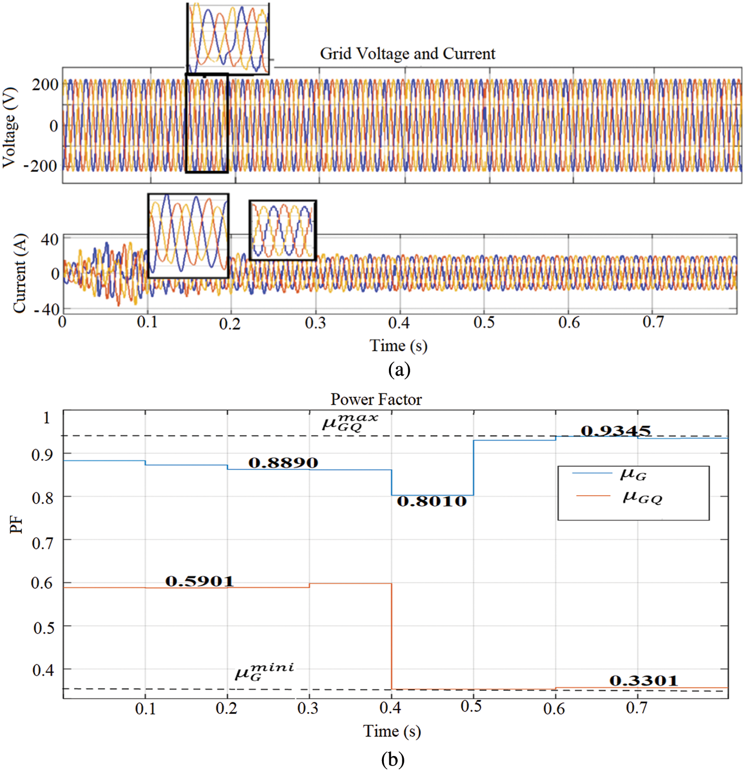

Figure 7: (a) PCC voltage and current (b) Power factor (c) Conformity factors

Figure 8: PCC voltage, grid and RDG current
6.2 Scenario 2: Balanced AC Voltages with RDG Active Power
The voltages are maintained sinusoidal and symmetric similar to scenario 1, RDG does not generate active power to the grid at the PCC while it is allowed to pre-compensate for the grid reactive power. The same condition for scenario 1 is also applied such that that
6.3 Distorted and Symmetrical Voltages without RDG’s Power to the Grid
This section discusses the outcome of the simulation when additional industrial or commercial loads are added to the network and observe if the proposed method is adequate and firm under such operation. The order of pre-compensation as scenario 1 is followed such that
6.4 Balanced AC Voltages with RDG Active Power Generation
This section discusses the simulation outcome when RDG generates active power to the network and the voltages are kept sinusoidal and symmetrical. The measured voltages in various buses are shown Table 1 and its graphical representation in Fig. 9. The system voltage profiles improved significantly with increase in the RDG penetration level. The voltage at the bus 9 (PCC) is slightly more than other buses voltage because of the active power generated by the RDG. The influence of the RDGs is obvious at the PCC’s voltage and the nearest buses. The network voltage profiles are within an acceptable limit as indicated by IEEE 1547 and the South Africa grid code act. The research work carried out in this paper showed that with the increase in RDG penetration level, there is an improved in the system voltage profiles in Fig. 9a which is also established in the research work carried out in [41]. Consequently, the weak network becomes an active system while incorporating an automation system, capable of monitoring power flows from points of generation to points of consumption. The measured values across the system buses at 69% penetration level causes an over-voltage as shown in Fig. 9b while the simulation result at t = 0.6 s around the PCC and in the grid are shown in Fig.10. At 1 s, the rise in voltage is higher on phases A and C while phase B voltage is within an acceptable range when the RDG’s penetration is 40% as observed in the grid. It is also observed that the voltages of all the phases are distorted, unbalanced, and the over-voltage is higher between 1 to 1.5 s, at 69% penetration at PCC which can be observed in Fig. 10. Morealso, the distortion increases when the connected loads drawn more current, phase shifted and unbalanced, then, harmonics current increases progressively. When the order of compensation is carried out with active power filter strategy only, such that


Figure 9: (a) Improved voltage profile with RDG (b) Voltage rise

Figure 10: Grid and PCC voltage rise
6.5 Balanced AC Voltages with FBMC Connection at PCC
This section presents the dynamic operation and performance analysis for reactive power generation/absorption and voltage control of proposed FBMC at PCC. Its act as a compensator to manage power quality challenges at PCC with RDG integration. The key purpose of employing the compensator is to improve the voltage rise, unbalanced current, minimize distortion and reactive power control at the PCC without RDG disconnection, to increase power flow capacity, release thermal capacity, reduce unbalance voltage/current, minimize harmonic and losses. Power transfer ability and grid strengthening should be enhanced with RDG integration to the power system without negative impacts. Usually, power quality problem arises in power system network due to the reactive power loss [42]. To achieve this aim, the dynamic performance analysis of the (FBMC) is investigated at PCC without RDG connection to the network and the simulation is carried out in the MATLAB/Simulink environment. The simulation analysis is depicted in Fig. 11, the proposed model has the capability to cope with voltage drops, unbalanced current/voltage originating from switching electrical loads and when the power supply is reduced due to intermittent of RDG. It possesses the ability to generate and absorb reactive power with fast response, which is performed through its phase reactance. The device behaves like inductance when the PCC voltage increases than the device voltage, it absorbs reactive power. But when PCC voltage is lower than the voltage of the device, it behaves like a capacitor thereby generating reactive power and it can also be regulated individualistically of the AC system voltage. Fig. 11a depicts the steady state operation strategy control of FBMC when the simulation run for at 0.1 s, where it produces in-phase voltage waveform with the PCC voltage such that the voltage generated is equal in magnitude to network voltage where there is no voltage rise issues and with zero current output, it does not absorb nor provide reactive power to the network. It is observed between 0 to 0.02 s, flow of switch-on surge current occurs, the FBMC quickly generates reactive power immediately to reduce the switching losses, its voltage is slightly increased than the PCC voltage which shows a fast response attribute of the device and quickly maintain the network voltage when the current goes off at t = 0.02 s. FBMC generates reactive power that is capacitive with leading output current flows across the grid and maintains zero after 0.02 s, showing that there is no exchange of power across the grid and there is no voltage rise occurrence at PCC above 0.02 s. The simulation results in Figs. 11b–11d depict the reactive power capability of the device when operating as purely inductive, capacitive, and as both such that, it generates a voltage waveform lower in magnitude than the network, enable the FBMC to perform as an inductive device and absorbing reactive power from the PCC. Likewise, it generates a voltage waveform higher in magnitude than the network, enable the FBSMC act as a capacitive device and generating reactive power to the grid.

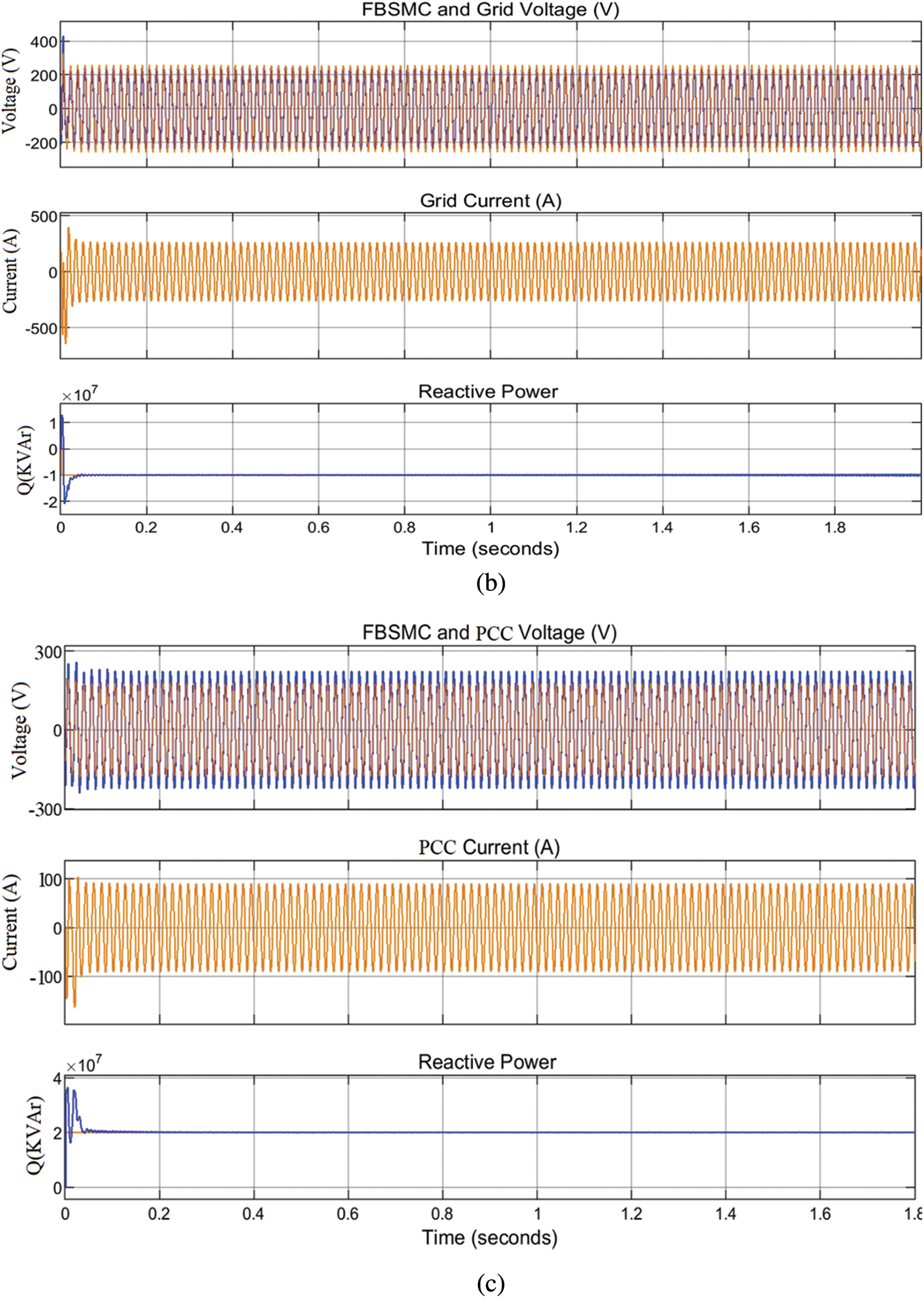
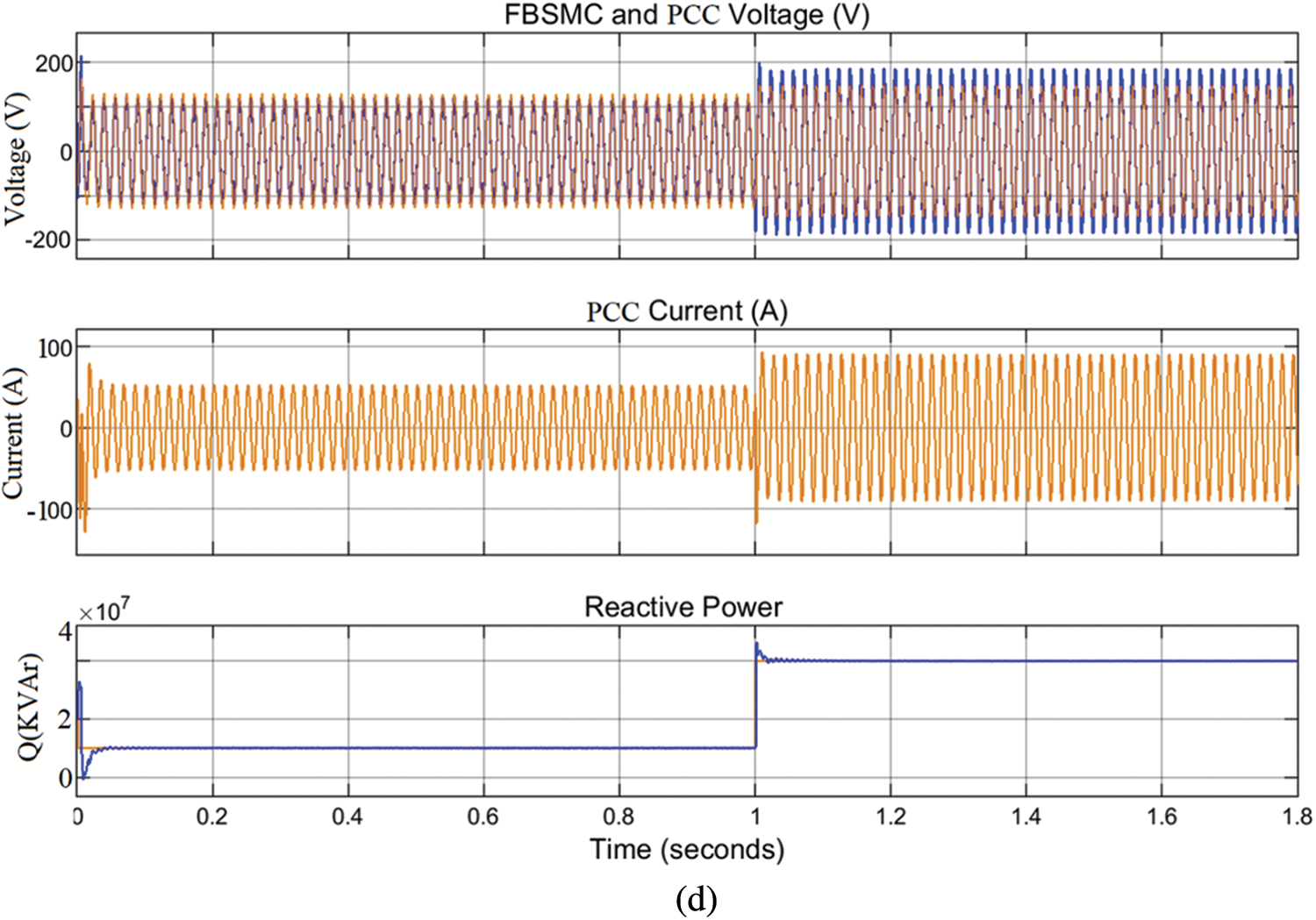
Figure 11: (a) FBMC in-phase voltage with PCC voltage, grid current and reactive power (b) FBSMC acts as inductive (c) FBMC acts at capacitive (d) FBMC acts as both
6.6 Reactive Power/Voltage Control at PCC
This section presents the impact of reactive power generation/absorption capability of FBMC at PCC when unbalanced and voltage rise occurs. For the coordination of the voltage control techniques at the PCC, online communication strategy is established between RDG units for the compensator to sense and communicate in case there is any voltage discrepancies or grid fault. The performance evaluation is carried out in the entire simulation 1.8 s at the PCC under normal operation condition. Integration of RGD to the network improves the network voltage profile while active power in Fig. 12a is being delivered to the grid, but when the penetration levels reach 69%, voltage rise occurs at the PCC as shown in Tables 1 and 2 of the voltage (per unit) measured across the buses of the network. IEEE-1547-2013 recommends disconnecting RDG at PCC whenever a voltage rise occurs to avoid distraction and damage to power equipment, whereas IEEE-1547-2018 recommends voltage rises regulation criteria at PCC, allowing RDG to ride through and remain connected [43,44]. At the 120% penetration levels of RDG into the network, the PCC voltage increases above 10% percent of its nominal value rating and the voltage rise in Figs. 12b–12e is not acceptable by the IEEE-1547-2013 specification, it is either the device is disconnected, or the voltage is regulated to an acceptable limit as specified by IEEE-1547-2018/2020. To compensate for the rise in voltage at PCC, FBMC is connected at PCC and the simulation procedures are repeated for 1.8 s. The simulation results are depicted in Figs. 12f–12i for 69% and 120% RDG penetration, respectively. The FBMC compensates for the voltage increase at PCC by absorbing reactive power from the PCC, such that the value of the reactive power absorbed by the device is equal to +0.18 Mvar at 1 s. The more RDG penetration at PCC, the more voltage rise overshoot increases the more FBMC compensate for this voltage increase by absorbing reactive power of +0.18 Mvar at 0.4 s in Figs. 12j–12m. The dynamic performance of the device is demonstrated at t = 1, when the device increases the reactive power for compensation from +0.18 Mvar to 0.2 Mvar. The calculated load current unbalance ratio is estimated to be 20%, the source current is quickly corrected to nearly balanced, and the source current unbalance ratio is improved to 2%. The converter produces the respective low-order harmonics with almost the same magnitude, hence, avoids them to appear in the output voltage. It shows that the highest low order harmonics having 12% with respect to the fundamental, while the harmonics lower than the 13% are successfully eliminated by the proposed method. FBMC produces high-quality AC and DC side waveforms, as well as a large number of output voltage levels per phase, the total voltage across the half bridge and full bridge chain-links of each arm are tightly controlled around the desired set-points. The total obstructing voltage of each half bridge chain-link in the FBMC arm is the full pole-to-pole dc link voltage, while the total obstructing voltage of each full bridge chain in the FBMC arm is half of the half bridge cell capacitor voltage. As a result, the total semiconductor loss associated with the addition of these extra full bridge chain-links is reduced. The full bridge chain-links function as active power filters, generating anti-phase voltage harmonics to cancel out the inherent harmonics in the arm voltages generated by the half bridge chain-links. The implementation of the proposed FBMC is exceedingly excellent considering the rapid reference tracking, fast response and convergence as shown in Fig. 12n. The assessment of THD during the voltage rise at PCC is depicted in Table 3. It is evidence that the voltage THD of the proposed FBMC at PCC during the occurrence of voltage rise is 0. 21% as compared to the inbuilt active power filter of the RDG which agrees with the IEEE requirements. Fig. 12m depicts the PCC and the grid voltage after the compensation activities. It shows that the over voltage, current ripples and the THD in the grid drop substantially faster while power quality remains within acceptable limit which agrees to the IEEE standard. The THDs analysis during the voltage rise, the compensating activities and the system measure voltages are shown in Tables 1–3, respectively. The FBMC continuously damps the PCC voltage rise, distortion, unbalanced current and harmonics during the PCC and grid disturbance. It supports the grid power quality parameters and maintains the network voltage throughout the simulation activities. Fig. 13 shows the sequence workflow of the simulations.
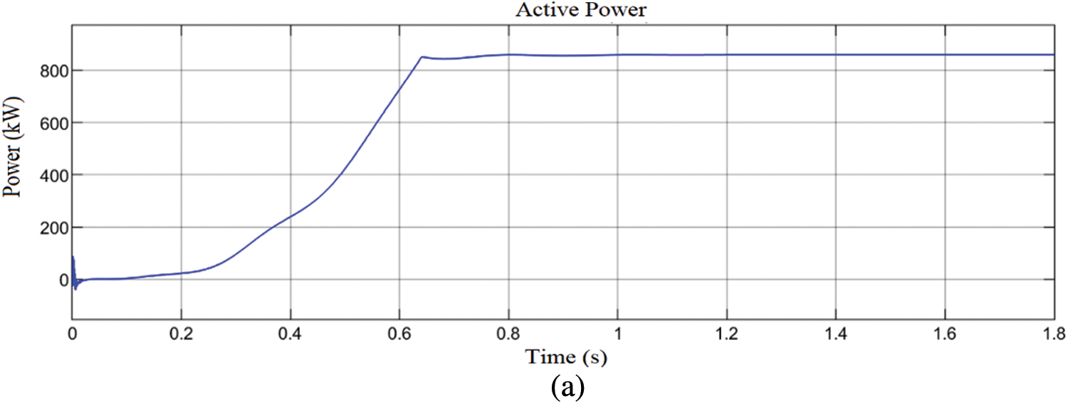
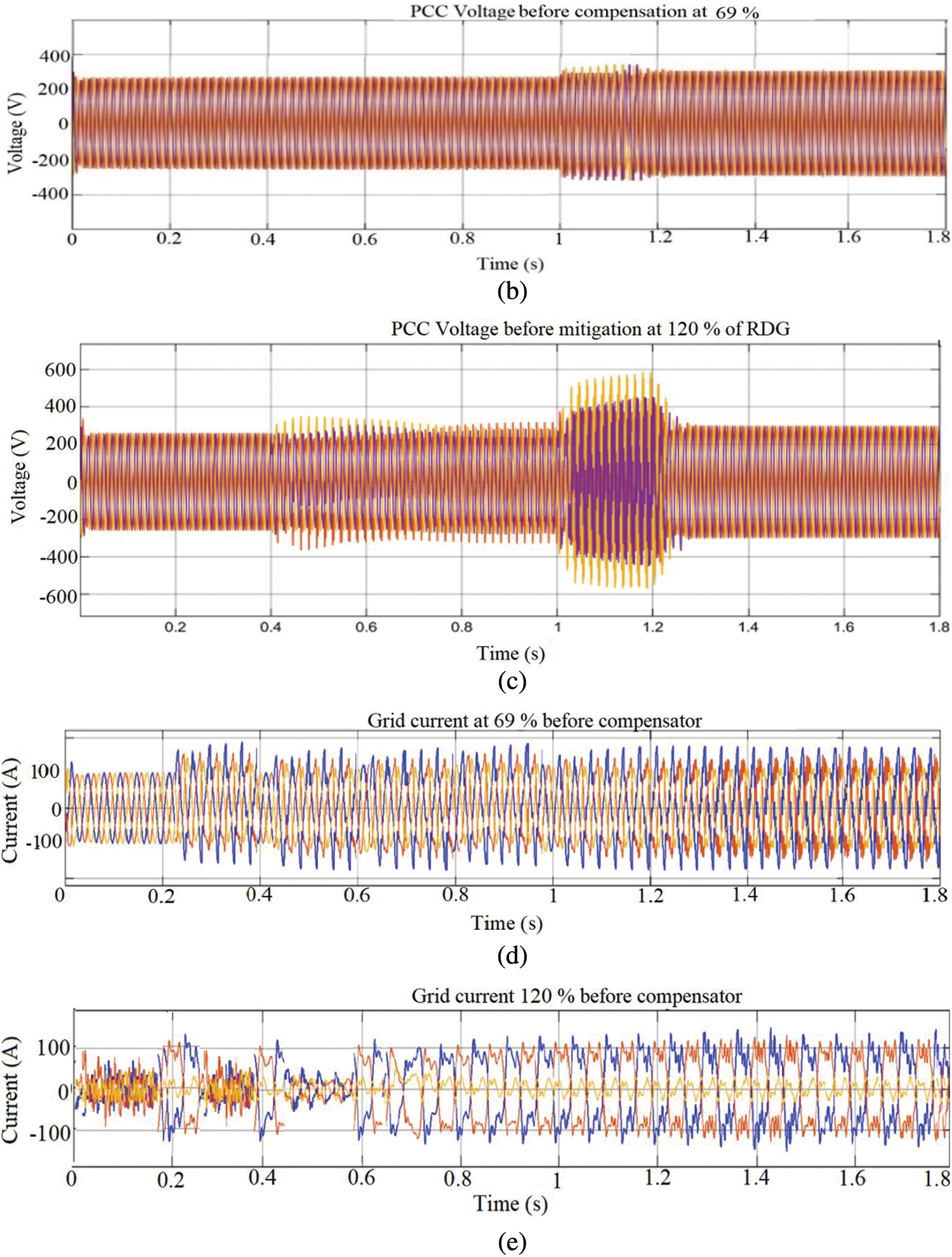


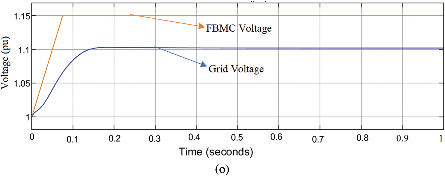
Figure 12: (a) Active power supplied to the grid (b) PCC voltage at 69% RDG before compensation (c) PCC voltage at 120% RDG before compensation (d) Grid current at 69% RDG before compensation (e) Grid current at 120% before compensation (f) PCC voltage at 69% RDG after compensation (g) PCC voltage at 120% RDG after compensation (h) Grid current at 69% RDG after compensation (i) Grid current at 120% after compensation Integration (j) FBMC current during compensation at 69% RDG (k) FBMC current during compensation at 120% (l) FBMC reactive power compensation at 69% RDG (m) FBMC reactive power compensation at 120% RDG (n) PCC voltage and FBMC voltage during compensation (o) Grid voltage and PCC voltage after compensation


Figure 13: Workflow chart
Sensitivity analysis of the FBMC is the study of how uncertainty in the output of a model can be apportioned to different sources of uncertainty in the model input [45], it is the measure of the effect of a given input on a given output. i.e., how sensitive the output is to a perturbation of the input. Each phase of FBMC is made up of two arms, each with three power cells (sub-module). A single power cell, as shown in Fig. 4, is made up of a DC capacitor, arm inductance, and four semiconductor switches that form a bidirectional chopper-cell. In addition to the main parameters, the power cell includes a dc-link capacitor, insulated gate bipolar transistor (IGBT) stray inductances, and busbar inductance. When the output is chosen to be the peak voltage across semiconductor devices of each sub-module, sensitivity analysis is performed at three different levels of sub-module, arm, and phase to predict the maximum voltage stress across semiconductor devices in the FBMC. The first order index of a power cell's dc-link capacitor, busbar stray inductance, IGBT stray inductance, and fall time is approximately 0.39, 0.119, 0.079, and 0.519, respectively, while the other switch parameters are less than 0.03. This indicates that, excluding the dc capacitance, busbar and IGBT stray inductances, and IGBT fall time, the relative merits of all parameters of a single power cell is negligible in establishing the power cell's peak voltage. Although the FBMC has nonlinear and time variant behavior as long as we are far away from the converter's resonant point. This paper's analysis is limited to only one switch in each sub-module. Switch 2 produces the same result. However, the busbar stray inductance for switches 3 and 4 would be different. This difference could be attributed to the different current commutation loops that each switch has when turned off.
The proposed strategy employed in this research paper successfully managed the PCC’s power quality to an acceptable range in relation to IEEE and South Africa grid voltage requirement. It limits the unbalanced current, distortion and voltage rise regulation at the PCC. It regulates the grid reactive power flow and minimizes the unbalanced current and distortion generated from the non-linear load. In steady state, the FBMC voltage and current at PCC has very low THD <0.4% and negative or zero sequence 0.0048 pu even with high penetration of RDG without any passive filter. The active power filter and FBMC utilized was able to compensate for the power quality challenge under grid disturbances such as voltage rise, unbalance load conditions. The FBMC's dynamic performance in terms of reactive power generation/absorption is adequate, with a fast response. The network accepts high concentration of RDG penetration power at PCC without disconnecting, while FBSMC regulates the voltage rise, harmonics distortion, unbalanced current and reverse power flow to be within an acceptable limit. The simulation analysis and experiment tests are presented over the whole power range and various operating modes. The results show that the proposed FBMC successfully mitigates the circulating fault current level, over-voltage, unbalance current and distortion. The FBMC enables more RDG penetrations into the network without overvoltage at the PCC, unbalanced current, or harmonic distortions to the system. The FBMC possesses a very high response time, higher accuracy, and harmonic mitigation capability as compared to active power filter. The application of voltage rise, revers power flow and distortion in different situations would have different impacts on the power flow at PCC and the grid if not for the variety of reactive power regulation and voltage rise control strategies at PCC for RDG integration to the power system. According to the findings of the paper, if the regulation capability of the active filter and FBMC are taken into account when determining the most practical and efficient method of regulating PCC voltage rise and distortion, the latter may be preferred. It has been demonstrated that the FBMC has the potential to reduce power circuit complexity, which is critical for condition monitoring and the protection of high-value assets such as high voltage direct current devices.
Funding Statement: The authors received no specific funding for this study.
Conflicts of Interest: The authors declare that they have no conflicts of interest to report regarding the present study.
References
1. Rezkallah, M., Chandra, A., Singh, B., Singh, S. (2019). Microgrid: Configurations, control and applications. IEEE Transaction on Smart Grid, 10(2), 1290–1302. DOI 10.1109/TSG.2017.2762349. [Google Scholar] [CrossRef]
2. Mohammad, S. G., David, J. H., Mehdi, B. (2021). A secondary control method for voltage unbalance compensation and accurate load sharing in networked microgrids. IEEE Transaction on Smart Grid, 12(4), 2822–2833. DOI 10.1109/TSG.2021.3062404. [Google Scholar] [CrossRef]
3. Ndamulelo, T., Ali, N. H., Thokozani, S. (2021). A fault level-based system to control voltage and enhance power factor through an on-load tap changer and distributed generators. IEEE Access, 9, 34023–34039. DOI 10.1109/ACCESS.2021.3061622. [Google Scholar] [CrossRef]
4. Bajaj, M., Singh, A. K. (2022). Optimal design of passive power filter for enhancing the harmonic-constrained hosting capacity of renewable DG systems. Computers and Electrical Engineering, 97, 107646. DOI 10.1016/j.compeleceng.2021.107646. [Google Scholar] [CrossRef]
5. Bajaj, M., Singh, A. K. (2022). Performance assessment of hybrid active filtering technique to enhance the hosting capacity of distorted grids for renewable energy systems. International Journal of Energy Research, 46(3), 2783–2809. DOI 10.1002/er.7345. [Google Scholar] [CrossRef]
6. IEEE (2019). IEEE approved draft guide for the application of shunt power capacitors. IEEE P1036/D9, 1–98. [Google Scholar]
7. Kalair, A., Abas, N., Kalair, A. R., Saleem, Z., Khan, N. (2017). Review of harmonic analysis, modeling and mitigation techniques. Renewable and Sustainable Energy Review, 78, 1152–1187. DOI 10.1016/j.rser.2017.04.121. [Google Scholar] [CrossRef]
8. Velásquez, M. A., Lara, V. M. (2019). Explosion of power capacitors in a change of transformers with reactive power compensation. Engineering Failure Analysis, 106, 104181. [Google Scholar]
9. Moreira, A. C., Paredes, H. K., Souza, W. A., Marafão, F. P., Silva, C. P. (2018). Intelligent expert system for power quality improvement under distorted and unbalanced conditions in three-phase AC micro-grids. IEEE Transaction on Smart Grid, 6(6), 6951–6960. [Google Scholar]
10. Moreira, A. C., Souza, W. A., Conrado, B. R., Morales-Paredes, H. K. (2022). Disturbing load classification based on the grey relational analysis method and load performance index. Journal of Control Automation and Electrical System, 31(1), 141–152. DOI 10.1007/s40313-019-00511-9. [Google Scholar] [CrossRef]
11. Arbab-Zavar, B., Palacios-Garcia, E., Vasquez, J., Guerrero, J. (2019). Smart inverters for microgrid applications: A review. Energies, 12(5), 840. DOI 10.3390/en12050840. [Google Scholar] [CrossRef]
12. Wang, L., Lam, C. S., Wong, M. C. (2018). Analysis, control, and design of a hybrid grid-connected inverter for renewable energy generation with power quality conditioning. IEEE Transaction on Power Electronics, 33(8), 6755–6768. DOI 10.1109/TPEL.2017.2753838. [Google Scholar] [CrossRef]
13. Mohamed, H. H., Salah, K., Mahmoud, A., Tahir, K., José, L. D. et al. (2021). Optimal reactive power dispatch with time-varying demand and renewable energy uncertainty using Rao-3 algorithm. IEEE Access, 9, 23264–23283. DOI 10.1109/ACCESS.2021.3056423. [Google Scholar] [CrossRef]
14. Sakib, M. N., Azad, S. P., Kazerani, M. (2022). A critical review of modular multilevel converter configurations and submodule topologies from DC fault blocking and ride-through capabilities viewpoints for HVDC applications. Energies, 15(11), 4176. DOI 10.3390/en15114176. [Google Scholar] [CrossRef]
15. Wang, K., Song, Q., Xu, S. (2022). Analysis and design of the energy storage requirement of hybrid modular multilevel converters using numerical integration and iterative solution. Energies, 15(3), 1225. DOI 10.3390/en15031225. [Google Scholar] [CrossRef]
16. Bajaj, M., Kumar, A. (2020). Singh grid integrated renewable DG systems: A review of power quality challenges and state-of-the-art mitigation techniques. International Journal of Energy Research, 44(1), 26–69. DOI 10.1002/er.4847. [Google Scholar] [CrossRef]
17. Zabihinejad, A., Viarouge, P. (2018). Global optimization of high-power modular multilevel active-front-end converter using analytical model. Electrical Engineering, 100(2), 509–518. DOI 10.1007/s00202-017-0523-5. [Google Scholar] [CrossRef]
18. Zhang, Y., Adam, G. P., Lim, T. C., Finney, S. J., William, B. W. (2012). Analysis of modular multilevel converter capacitor voltage balancing based on phase voltage redundant states. IET Power Electronics, 5(6), 726–738. DOI 10.1049/iet-pel.2010.0305. [Google Scholar] [CrossRef]
19. Adam, G. P., Anaya-Lara, O., Burt, G. M., Telford, B. W., Williams, D. et al. (2010). Modular multilevel inverter: Pulse width modulation and capacitor balancing technique. IET Power Electronics, 3(5), 702–715. DOI 10.1049/iet-pel.2009.0184. [Google Scholar] [CrossRef]
20. Giddani, O. A., Adam, G. P., Anaya-Lara, O., Burt, G., Lo, K. L. (2010). Control strategies of VSC-HVDC transmission system for wind power integration to meet GB grid code requirements. International Symposium on Power Electronics, Electrical Drives, Automation and Motion (SPEEDAM), pp. 385–390. Pisa, Italy. DOI 10.1109/SPEEDAM.2010.5542237. [Google Scholar] [CrossRef]
21. Du, S., Liu, J., Liu, T. (2014). Modulation and close-loop based DC capacitor voltage control for MMC with fundamental switching frequency. Power Electronics, IEEE Transactions, 30(1), 327–338. [Google Scholar]
22. Hagiwara, M., Akagi, H. (2009). Control and experiment of pulse width-modulated modular multilevel converters. Power Electronics, IEEE Transactions, 24(7), 1737–1746. DOI 10.1109/TPEL.2009.2014236. [Google Scholar] [CrossRef]
23. Parvin, K., Hossain-Lipu, M. S., Hannan, M. A., Abdullah, M. A., Jern, K. P. et al. (2021). Intelligent controllers and optimization algorithms for building energy management towards achieving sustainable development: Challenges and prospects. IEEE Access, 9, 41577–41602. DOI 10.1109/ACCESS.2021.3065087. [Google Scholar] [CrossRef]
24. Sajjad, H., Milad, Z. M., Behrooz, B. (2021). Optimal allocation and sizing of synchronous condensers in weak grids with increased penetration of wind and solar farms. IEEE Journal on Emerging and Selected Topics in Circuits and Systems, 11(1), 199–209. DOI 10.1109/JETCAS.2021.3053554. [Google Scholar] [CrossRef]
25. Tenti, P., Paredes, H. K., Mattavelli, P. (2011). Conservative power theory, a framework to approach control and accountability issues in smart microgrids. IEEE Transaction on Power Electronics, 26(3), 664–673. DOI 10.1109/TPEL.2010.2093153. [Google Scholar] [CrossRef]
26. Tenti, P., Mattavelli, P., Morales-Paredes, H. K. (2010). Conservative power theory, sequence components and accountability in smart grids. International School on Non-Sinusoidal Currents and Compensation, Lagow, Poland. [Google Scholar]
27. Souza, W. A., Liberado, E. V., Silva, L. C., Marafão, F. P., Morales-Paredes, H. K. (2013). Load analyzer using conservative power theory. International School on Non-Sinusoidal Currents and Compensation, Zielona, Gora. [Google Scholar]
28. Liu, J., Zhao, C. C., Xie, Z. H. (2021). Power and current limiting control of wind turbines based on PMSG under unbalanced grid voltage. IEEE Access, 9, 9873–9883. DOI 10.1109/ACCESS.2021.3049839. [Google Scholar] [CrossRef]
29. Oscar, C. Z., Jose, B. D., Fernando, M. D., Francisco, A. S., Rafael, C. N. (2021). Control of photovoltaic inverters for transient and voltage stability enhancement. IEEE Access, 9, 44363–44373. DOI 10.1109/ACCESS.2021.3066147. [Google Scholar] [CrossRef]
30. Gyu, S. L., Pyeong-Ik, H., Seung, M. (2021). Reactive power control of hybrid multi-terminal HVDC systems considering the interaction between the AC network and multiple LCCs. IEEE Transactions on Power Systems, 36(5), 4562–4574. DOI 10.1109/TPWRS.2021.3056565. [Google Scholar] [CrossRef]
31. Peng, L., Grain, P. A., Derrick, H., Barry, W. (2021). Controlled transition full-bridge hybrid multilevel converter with chain-links of full-bridge cells. IEEE Transactions on Power Electronics, 36(1), 23–38. [Google Scholar]
32. Hamasaki, S., Hadano, K., Eguchi, S., Tsuji, M. (2016). Control of full bridge type modular multilevel converter for single phase AC/AC conversion. International Conference on Electrical Machines and Systems (ICEMS), Chiba, Japan. [Google Scholar]
33. Miodrag, B., Dražen, D. (2021). Hybrid modular multilevel converter for variable DC link voltage operation. CPSS Transactions on Power Electronics and Applications, 6(2), 178–190. DOI 10.24295/CPSSTPEA.2021.00016. [Google Scholar] [CrossRef]
34. Zhang, Y., Zhang, J., Deng, F., Xu, Z., Zhao, J. (2021). Hybrid modular multilevel converter with self-balancing structure. IEEE Transactions on Industry Applications, 57(5), 5039–5051. DOI 10.1109/TIA.2021.3087669. [Google Scholar] [CrossRef]
35. Chen, Y., Pan, S., Huang, M., Zhu, Z., Liu, Y. et al. (2021). MMC-MTDC transmission system with partially hybrid branches. CES Transactions on Electrical Machines and Systems, 5(2), 124–132. DOI 10.30941/CESTEMS.2021.00016. [Google Scholar] [CrossRef]
36. Mohamed, A., Yousef, N., Fahad, A., Khaled, H., Ayman, S. et al. (2021). A new hybrid dual active bridge modular multilevel based DC-DC converter for HVDC networks. IEEE Access, 9, 62055–62073. DOI 10.1109/ACCESS.2021.3074543. [Google Scholar] [CrossRef]
37. IEEE (2020). IEEE standard for interconnection and interoperability of distributed energy resources with associated electric power systems interfaces—Amendment 1: To provide more flexibility for adoption of abnormal operating performance category III. IEEE. [Google Scholar]
38. Thakur, S. S., Odavic, M., Allu, A., Zhu, Z. Q., Atallah, K. (2022). Analytical modelling and optimization of output voltage harmonic spectra of full-bridge modular multilevel converters in boost mode. IEEE Transactions on Power Electronics, 3(37), 3403–3420. DOI 10.1109/TPEL.2021.3108877. [Google Scholar] [CrossRef]
39. Bojoi, R. I., Limongi, L. R., Roiu, D., Tenconi, A. (2011). Enhanced power quality control strategy for single-phase inverters in distributed generation systems. IEEE Transactions on Power Electronics, 26(3), 798–806. DOI 10.1109/TPEL.2010.2103572. [Google Scholar] [CrossRef]
40. Sakulphaisan, G., Junhuathon, N., Chayakulkheeree, K. (2022). Minimizing power loss in a DC distribution system through an analysis of the loss sensitivity factor and distributed generator loss characteristics. International Electrical Engineering Congress (IEECON), Khon Kaen, Thailand. [Google Scholar]
41. Akinyemi, A. S., Musasa, K., Davidson, I. E. (2022). Analysis of voltage rise phenomena in electrical power network with high concentration of renewable distributed generations. Scientific Reports, 12(1), 7815. DOI 10.1038/s41598-022-11765-w. [Google Scholar] [CrossRef]
42. Sultana, W., Jebaseelan, S. D. (2022). Improved grid power transmission using solar panel (PV-Statcom) in day and night. International Conference on Advances in Computing, Communication and Applied Informatics (ACCAI), Chennai, India. [Google Scholar]
43. IEEE (2020). IEEE approved draft standard for interconnection and interoperability of distributed energy resources with associated electric power systems interfaces-Amendment 1 to IEEE Std 1547-2018 to provide more flexibility for adoption of abnormal operating perf. IEEE. [Google Scholar]
44. IEEE (2022). IEEE draft application guide for IEEE Std 1547(TMIEEE standard for interconnecting distributed resources with electric power systems. IEEE. [Google Scholar]
45. Stefano, S. A., Campolongo, T. F., Ratto, M. (2004). Sensitivity analysis in practice: A guide to assessing scientific models. Ispra, Italy: John Wiley & Sons. [Google Scholar]
Cite This Article
 Copyright © 2022 The Author(s). Published by Tech Science Press.
This work is licensed under a Creative Commons Attribution 4.0 International License , which permits unrestricted use, distribution, and reproduction in any medium, provided the original work is properly cited.
 Downloads
 Citation Tools