
 Submit a Paper
 Propose a Special lssue
 Open Access
ARTICLE
A Novel Non-Isolated Cubic DC-DC Converter with High Voltage Gain for Renewable Energy Power Generation System
School of Electrical Engineering, Southwest Jiaotong University, Chengdu, 610036, China
* Corresponding Author: Yida Zeng. Email:
Energy Engineering 2024, 121(1), 221-241. https://doi.org/10.32604/ee.2023.041028
Received 08 April 2023; Accepted 14 July 2023; Issue published 27 December 2023
 View Full Text
 Download PDF
Abstract
In recent years, switched inductor (SL) technology, switched capacitor (SC) technology, and switched inductor-capacitor (SL-SC) technology have been widely applied to optimize and improve DC-DC boost converters, which can effectively enhance voltage gain and reduce device stress. To address the issue of low output voltage in current renewable energy power generation systems, this study proposes a novel non-isolated cubic high-gain DC-DC converter based on the traditional quadratic DC-DC boost converter by incorporating a SC and a SL-SC unit. Firstly, the proposed converter’s details are elaborated, including its topology structure, operating mode, voltage gain, device stress, and power loss. Subsequently, a comparative analysis is conducted on the voltage gain and device stress between the proposed converter and other high-gain converters. Then, a closed-loop simulation system is constructed to obtain simulation waveforms of various devices and explore the dynamic performance. Finally, an experimental prototype is built, experimental waveforms are obtained, and the experimental dynamic performance and conversion efficiency are analyzed. The theoretical analysis’s correctness is verified through simulation and experimental results. The proposed converter has advantages such as high voltage gain, low device stress, high conversion efficiency, simple control, and wide input voltage range, achieving a good balance between voltage gain, device stress, and power loss. The proposed converter is well-suited for renewable energy systems and holds theoretical significance and practical value in renewable energy applications. It provides an effective solution to the issue of low output voltage in renewable energy power generation systems.Keywords
The excessive utilization of conventional fossil fuels has been found to contribute significantly to the escalation of carbon emissions, thereby triggering a detrimental impact on the global environment, particularly through the exacerbation of global warming [1]. Moreover, due to the insufficient reserves of these traditional energy sources, the surging consumer demand remains unmet, necessitating the exploration of alternative avenues. Consequently, the pursuit of renewable energy sources has emerged as a paramount strategy to combat environmental pollution and address the ongoing energy crises, captivating the attention of researchers worldwide [2,3]. In order to facilitate the effective utilization of renewable energy, the development and implementation of renewable energy generation systems have become imperative. Nevertheless, the prevailing setback lies in the inability of current renewable energy generation systems to generate output voltage at levels sufficient to fulfill the requirements of the DC bus outputs [4,5]. This pressing challenge can be effectively surmounted through the application of DC-DC boost converter technology, as illustrated in Fig. 1. By employing the aforementioned DC-DC boost converter, the electricity derived from renewable energy sources can be effectively elevated to meet the voltage requirements of the DC bus, ensuring the smooth transmission of power to the load side. Consequently, the significance and demand for boost converters continue to experience an upward trajectory.
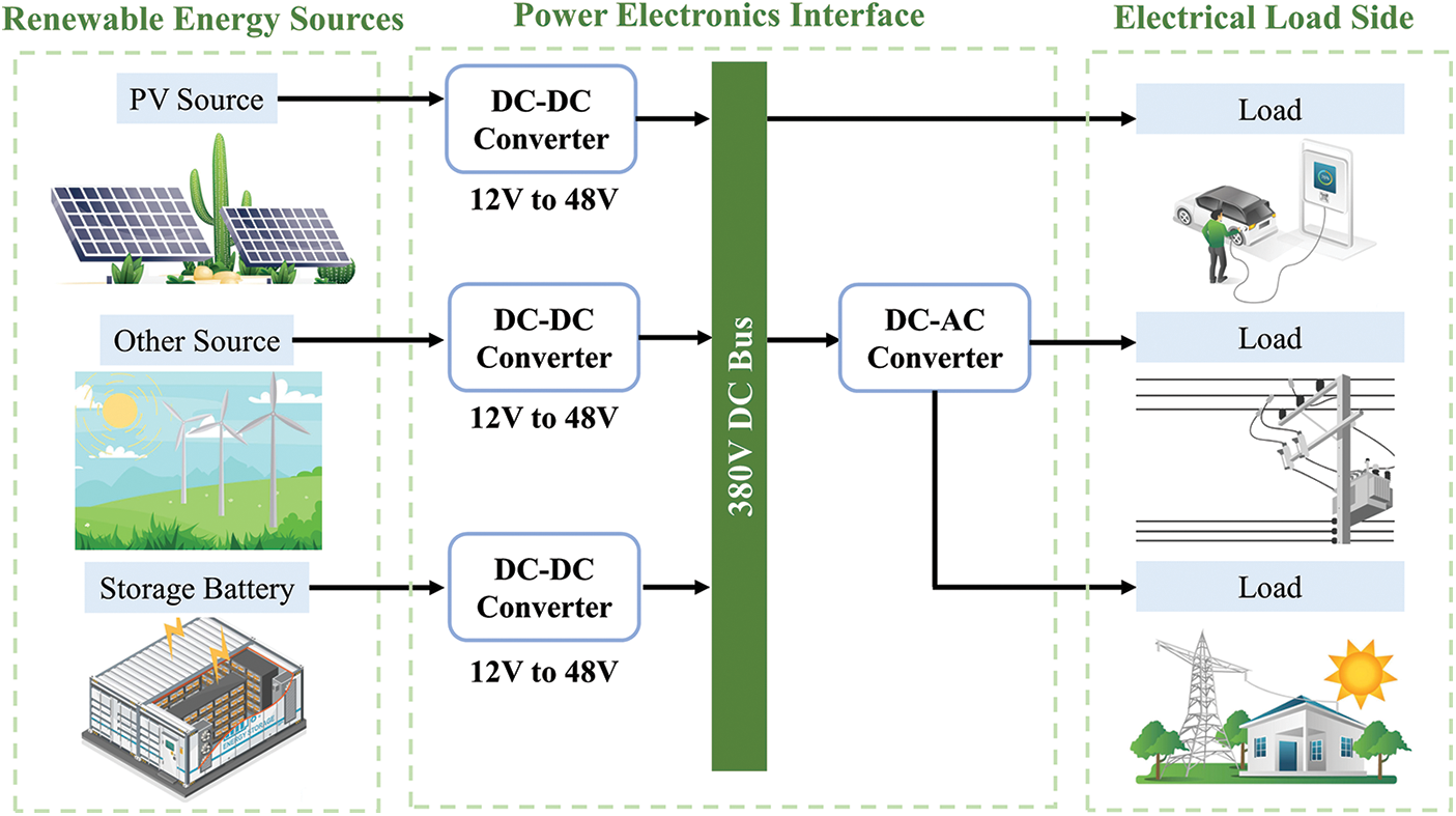
Figure 1: Typical application of DC-DC converter
Among the array of boost converters available, non-isolated DC-DC converters have garnered considerable interest owing to their relatively diminutive size, reduced losses, and cost-effectiveness [6]. With their uncomplicated structure and the ability to amplify voltage by adjusting the duty cycle, traditional non-isolated DC-DC converters have witnessed widespread adoption in industrial production settings [7]. The voltage gain ideally tends toward infinity as the duty cycle approaches unity. However, this amplified voltage gain can precipitate complications such as diode reverse recovery and transient response issues [8–10]. Additionally, the heightened current stress imposed on devices accentuates conduction losses, consequently impeding converter efficiency. Hence, while traditional DC-DC converters boast simplicity and affordability, their limited voltage boost ratio characteristics serve to restrict their range of application scenarios.
To achieve high voltage gain, researchers have conducted extensive investigations on high-gain DC-DC converters [11–14], such as quadratic DC-DC converters [15–17], two-switch DC-DC converters [18] and single-switch DC-DC converters [19–20]. For instance, references [21–23] proposed a cascade structure in the topology that enhances the overall output voltage by connecting two boost converters together in a back-to-back configuration. However, this particular topology necessitates the utilization of numerous components, engendering an enlargement in size, augmented costs, and increased power losses. References [24,25] introduced a quadratic DC-DC converter that exhibited high-voltage boost characteristics. Nonetheless, to attain a voltage gain of 10, this converter necessitates operation at an exceedingly high duty cycle, resulting in heightened device stress, which compromises the efficiency. The converter proposed in reference [26] attains an ultra-high voltage gain of 10 by operating at a duty cycle of 0.5. Alas, the associated topology manifests significant complexity, with the doubling unit alone comprising one inductor, three capacitors, and two diodes, resulting in a grand total of 18 components. As a consequence, this intricacy incurs elevated costs and power losses. Consequently, an only pursuit of voltage gains in DC-DC converters may inadvertently give rise to adverse implications such as escalated device stress and diminished conversion efficiency. Thus, for DC-DC boost converters, it is crucial to strike a balance among voltage gain, device stress, and power loss.
Switched-capacitor (SC) and switched-inductor (SL) technologies offer solutions to the above limitations. SC and SL possess the advantage of simple structures and low costs. The incorporation of SC and SL technology into a simple DC-DC boost converter holds the potential to optimize performance, enabling higher voltage gains while mitigating voltage stress on components. This approach facilitates the attainment of a harmonious balance between voltage gain, device stress, and power loss [12,20,27–30]. Furthermore, the amalgamation of SC and SL technology, leading to the emergence of switched inductor-capacitor (SL-SC) technology, presents an additional avenue to diminish voltage stress and power loss within DC-DC boost converters, attracting considerable attention in recent years [31–33]. Consequently, this paper proposes a novel cubic high-gain DC-DC boost converter that utilizes the incorporation of a SC unit and a SL-SC unit into the conventional quadratic DC-DC boost converter.
Section 2 provides a detailed description of the proposed converter, including its topology, operating mode, voltage gain, device stress, converter parameter design, and power loss. Section 3 presents an analysis that compares the converter in this paper with other converters. The simulation analysis results are presented in Section 4. Finally, Section 5 presents an experimental prototype that validates the theoretical analysis through experiments.
2 Details of the Proposed Converter
2.1 Configuration of the Proposed Converter
The topology of the proposed converter is illustrated in Fig. 2. This work suggests a novel non-isolated cubic DC-DC converter that incorporates a switched capacitor (SC) unit and a switched inductor-capacitor (SL-SC) unit into the traditional quadratic boost converter, resulting in a cubic boost ratio. SL-SC and SC may require more space due to the larger volume of inductors and capacitors. Additionally, fast charging and discharging in SL-SC and SC necessitate the use of high-speed switching devices, which may result in compromised performance and noise interference in high-frequency applications. Despite the aforementioned disadvantages of the converter, the advantages of the converter are significant, with the main benefits being:
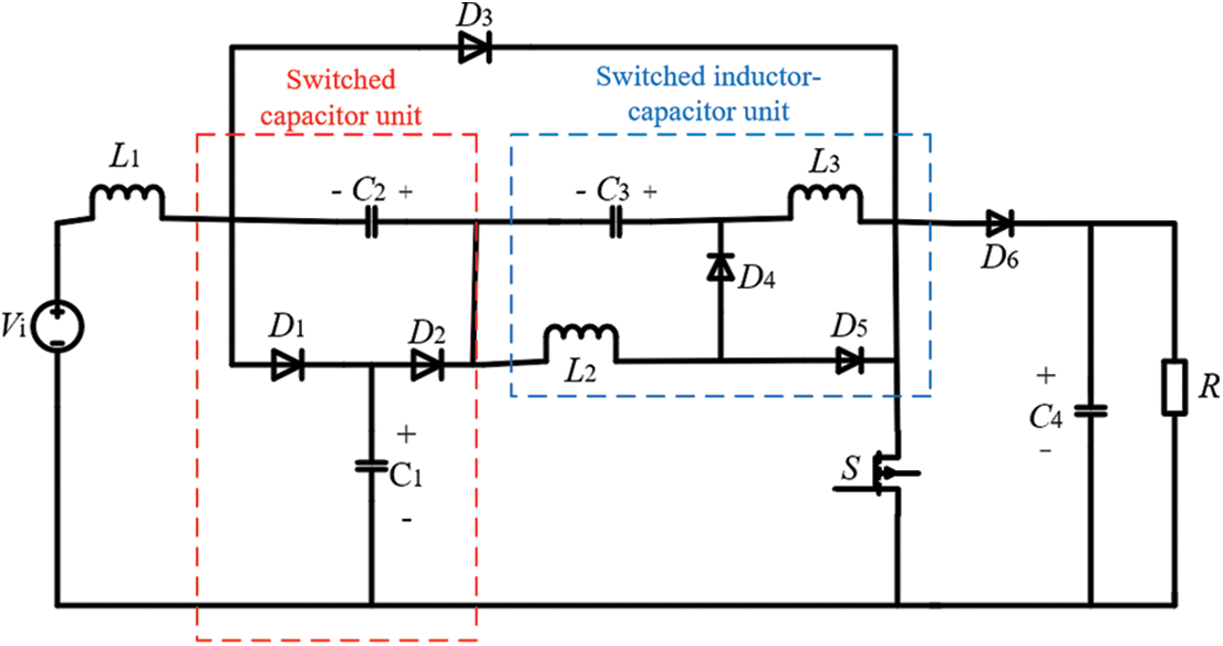
Figure 2: A novel non-isolated cubic DC-DC converter
(1) The converter delivers high voltage gain while maintaining low device stress and high conversion efficiency.
(2) The cubic voltage gain of the converter results in an extensive input voltage range.
(3) Utilizing a single switch structure simplifies the control of the converter.
(4) The converter requires fewer components than the high-gain converters presented in references [22] and [26].
(5) The input current remains continuous, with shared ground facilities between the input and load terminals.
The converter comprises a switch (S), inductors (L1–L3), capacitors (C1–C4), diodes (D1–D6), and a resistance (R). Fig. 3 illustrates the switching characteristics of the proposed converter. The analysis of the operating principle of the proposed converter in the subsequent sections is based on the hypotheses: (1) the switch and diodes are considered ideal devices, (2) the capacitance is sufficiently large to maintain the capacitance voltage constant for one cycle, and (3) inductors L1, L2, and L3 all function in continuous conduction mode (CCM).
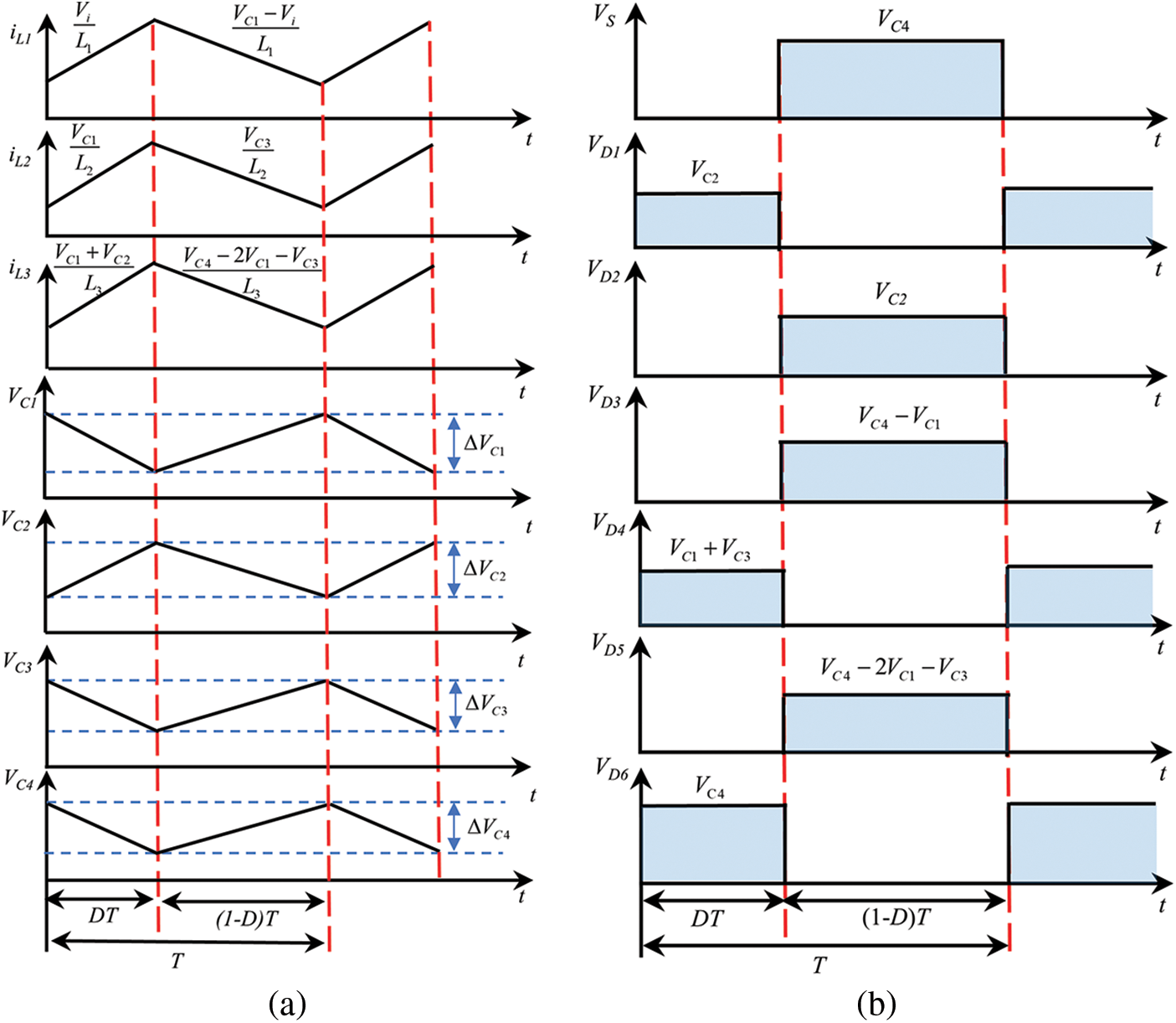
Figure 3: Switching characteristics of the converter: (a) Signals of reactive elements. (b) Signals of semiconductor elements
The converter features only one switch S, resulting in two operating modes within a single switching cycle TS, namely, conduction and off mode. Figs. 4 and 5 show the equivalent circuits of the two modes, with D representing the converter duty cycle. Detailed elaboration on the working principles of these modes will be provided in the subsequent sections.
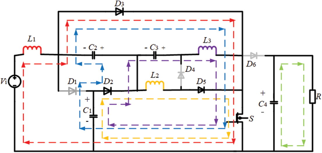
Figure 4: Switch tube conduction mode of the proposed converter, 0 < t ≤ DTS
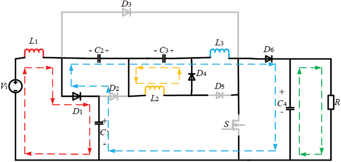
Figure 5: Switch tube off mode of the proposed converter, DTS<t ≤ TS
2.2 Switch Tube Conduction Mode
In the present mode (Fig. 4), the switch tube S is turned on, causing diodes D1, D4, and D6 to turn off by reverse voltage drop, while diodes D2, D3, and D5 turn on by forward voltage drop. The input voltage Vi transfers energy to the inductor L1; Capacitor C1 charges capacitor C2; The capacitor C1 charges the energy storage inductor L2; The capacitors C1 and C3 are connected in series to convey power to L3; The resistance R is powered by the capacitor C4. The waveform of inductive current iL1, iL2, and iL3 shows a linear upward trend. This process encompasses the following:
In switch tube off mode (Fig. 5), the switch tube S is turned off, D2, D3, and D5 are deactivated by withstanding a reverse voltage drop, and D1, D4, D6 are conducted by withstanding a forward voltage drop. The input voltage Vi and the input inductor L1 charge the capacitor C1; Vi, L1, C2, C3, L3 charge C4; L2 charges C3; The resistance R is powered by C4. The waveform of inductive current iL1, iL2, and iL3 shows a linear downward trend. This process includes:
Based on the volt-second balance principle on the inductors within a single switching period TS, we can deduce that:
The voltage stress equations for capacitors C1~C4 can be obtained from Eq. (3):
The mathematical expression for the voltage gain of the converter can be derived by using Eqs. (3)~(4):
where Vi, Vo, M, and D are the input voltage, output voltage, voltage gain, and duty cycle of the converter, respectively. Therefore, the final output voltage of the proposed converter can be calculated using the subsequent expression:
2.5 Calculation of Voltage Stress and Current Stress
In the conduction mode, the diodes D1, D4, and D6 are turned off; In the off mode, the diodes D2, D3, and D5 are turned off. The voltage across the switch tube S equals the voltage across the capacitor C4. The following formula is the voltage stress expression for switch tube S and diodes D1~D6:
According to the ampere-second balance principle on the capacitors, the current stress expressions for D1~D6 can be obtained:
The capacitive current stress can be obtained under the switch tube conduction and off mode:
The mean current passing through the switch during the conduction mode is:
2.6 Converter Parameter Design
Under lossless conditions, the input power and output power of the converter should be equivalent, so it can be expressed as:
According to the ampere-second balance principle on C3 and C4, and combining Eqs. (1)~(2), it can be obtained that:
The expressions of IL1~IL3 can be obtained from Eqs. (11)~(12):
After turning on the switch tube, the voltages of the inductors L1~L3 can be obtained from Eq. (1), and we can derive the formula for the inductor current ripple as follows:
According to the boundary conditions when the inductive current operates at CCM:
By substituting Eqs. (13)~(14) into Eq. (15), the subsequent expression can be derived:
After activating the switch tube S, the current of the capacitors C1 to C4 can be obtained from Eq. (9), and the expression of the capacitor voltage ripple is obtained as follows:
If the capacitance voltage ripple value does not exceed 1% of the average capacitance voltage, there are:
The converter’s power loss is composed of four primary components: capacitance loss, switch loss, diode loss, and inductance loss. Fig. 6 displays the equivalent circuit of the proposed converter, incorporating parasitic parameters, to investigate its power consumption. rs1 represents the parasitic resistance of the power switch, and ton and toff represent the conduction and off delay times of the switch, respectively. VF1~VF6 are the forward conduction voltage drops of diodes D1~D6, individually. rD1~rD6 are the forward conduction resistances of diodes D1~D6. rC1~rC4 represent the series parasitic resistance of capacitors C1~C4, respectively. rL1~rL3 represent the series parasitic resistance of inductors L1~L3, correspondingly.
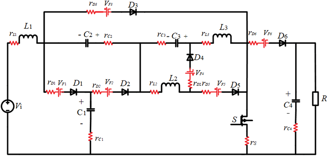
Figure 6: Equivalent circuit of the converter considering parasitic parameters
When S is activated, the power loss produced by it is primarily categorized into conduction and switching losses. The total loss of the switch tube can be calculated using Eq. (19). Where Vds and Id are the average voltage and average current of the switch tube, IS_rms represents the effective value of the switch current.
The power loss in diodes primarily results from forward conduction resistance and forward conduction voltage drop. The power loss of the diode can be calculated by Eq. (20). Where ID_ rms represents the effective value of diode current, ID_avg represents the average value of diode current.
The inductance loss and capacitance loss are mainly generated by their respective series parasitic resistors. The calculation formula is shown as Eq. (21). Where IL_ rms and IC_ rms represent the effective value of the inductive current and the effective value of the capacitive current, respectively.
The total power loss of the converter is:
The conversion efficiency of the converter can be obtained from Eq. (23), where Po represents the output power.
3 Comparison with Other Converters
The present study compares the voltage gain, switch voltage stress, and switch quantity of the proposed converter with other high-gain converters, as outlined in Table 1. For equitable comparison, this study selects the capacitor and the diode with the lowest stress values from each converter. The minimum voltage stress of the capacitor and diode for various converters is also presented in Table 1.
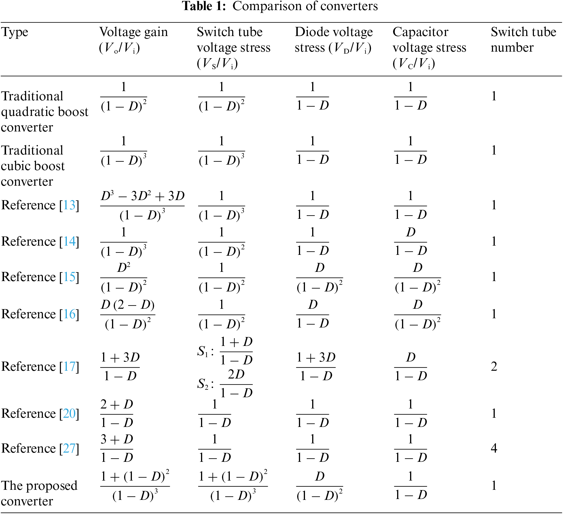
The findings indicate that the proposed converter offers decreased switch tube quantity and simpler control when compared to the references [17] and [27]. While the number of switching tubes in other references aligns with that in this study, there are variations in voltage gain and device stress. To provide a visual comparison, Figs. 7a~7d display the curve of voltage gain vs. duty ratio D (D = 0.2 to 0.7), the curve of diode stress vs. voltage gain, the curve of capacitor stress vs. voltage gain, and the curve of switch stress vs. voltage gain, respectively. Under the same duty ratio, the proposed converter has a larger gain value compared to converters [13–17,20,27], conventional quadratic boost converter and conventional cubic boost converter, as depicted in Fig. 7a. At a duty cycle of 0.4, the proposed converter achieves a voltage gain of 6.3, which is 1.73, 1.34, 3.57, 1.71, 1.56 and 1.17 times the voltage gain in references [13,14,16,17,20] and [27], respectively, and even 15.36 times the voltage gain in reference [15], reflecting the high gain advantage of the proposed converter. Furthermore, Figs. 7b and 7c suggest that the proposed converter provides the advantage of low voltage stress for the capacitor and diode. As depicted in Fig. 7d, the voltage stress on the power switch of the proposed converter is less than that in references [13,15–16], and is flush with traditional quadratic and traditional cubic boost converters. While the switch voltage stress in converters [14,17,20] and [27] is lower, these converters require higher duty ratios to obtain the desired voltage boost ratio. This can lead to transient response issues [19]. Additionally, the capacitor and diode stress in these converters is higher. Therefore, overall, when compared to other converters, the proposed converter offers significant advantages in terms of both device stress and voltage gain.
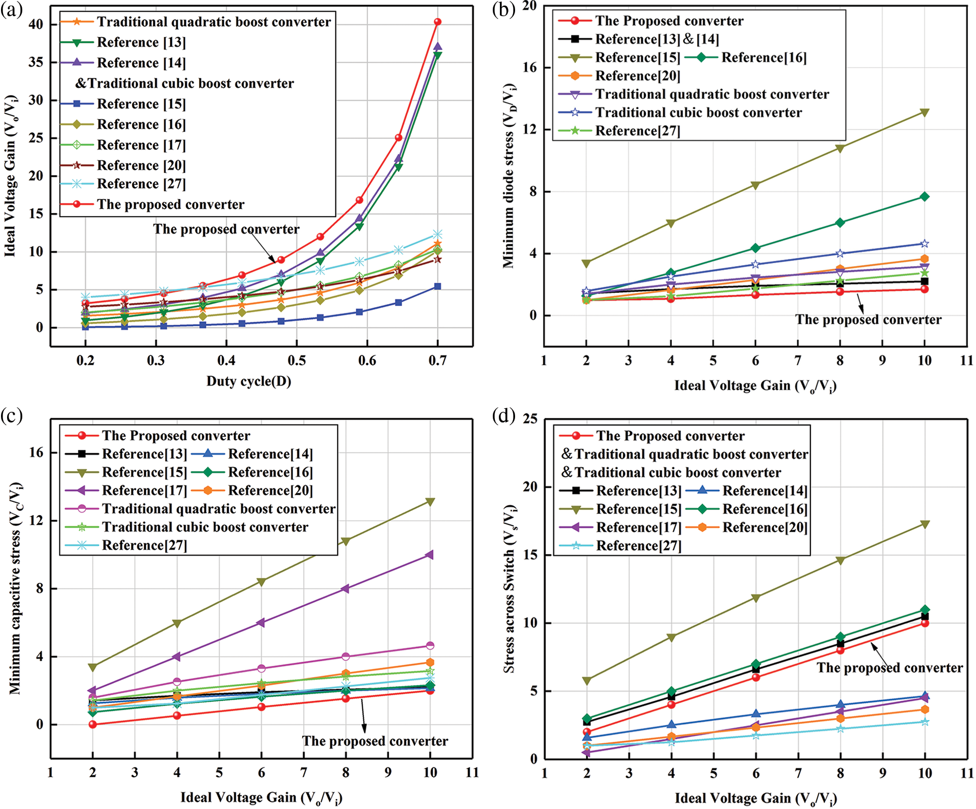
Figure 7: Comparison of converters: (a) voltage gain vs. duty ratio, (b) diode stress vs. voltage gain, (c) capacitor stress vs. voltage gain, (d) switch stress vs. voltage gain
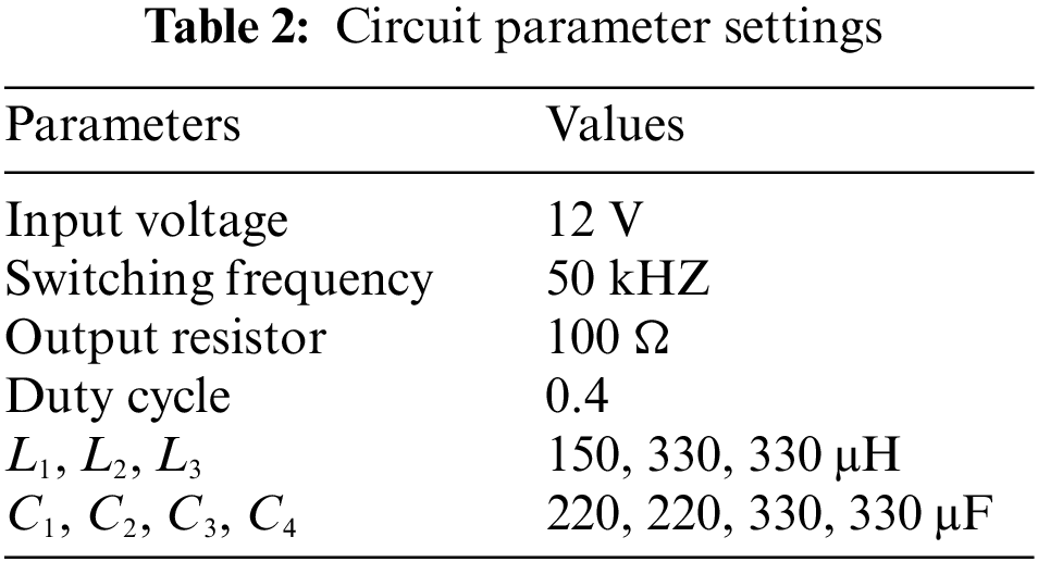
Table 2 lists the main circuit parameters for closed-loop simulation. The selection of inductor values L1, L2, and L3 considers the minimum inductance requirement specified in Eq. (16), while retaining a certain margin and taking into account cost and performance. Similarly, capacitor parameters C1, C2, C3, and C4 are chosen to meet the minimum capacitance value requirement stated in Eq. (18), while also retaining a certain margin and considering cost and performance.
The simulation waveforms of different devices with a duty ratio of 0.4 are presented in Fig. 8. Figs. 8a~8c indicate that the average currents of inductors L1, L2, and L3 are 4.71, 1.98, and 1.25 A, respectively, which are consistent with the results obtained from Eq. (13). Fig. 8a shows that the input current (equal to inductance L1 current) is essentially continuous, which is crucial for the application of new energy [20]. Additionally, the average output current is around 0.75 A, as shown in Fig. 8d, which confirms the theoretical analysis results. The capacitor voltage waveform is shown in Figs. 8e~8h, the average voltages of capacitors C1, C2, C3, and C4 are approximately 20, 20, 13.3, and 75.5 V, respectively, consistent with the theoretical analysis results obtained in Eq. (4). Figs. 8i~8p display the semiconductor voltage and output voltage waveforms. For the proposed converter, the load voltage is equal to the output voltage. According to Fig. 8j, the output voltage (load voltage) is around 75.5 V, which is achieved with an input voltage of 12 V. The voltage gain is 6.3. The simulation results verify the high-gain advantage of the proposed converter. Moreover, the voltage of the switch tube is about 75.5 V, as shown in Fig. 8i. The voltages of diodes D1, D2, D3, D4, D5, and D6 in Figs. 8k~8p are approximately 20, 20, 55.5, 33.3, 22.25, and 75.5 V, respectively, consistent with the theoretical calculation results in Eq. (7).
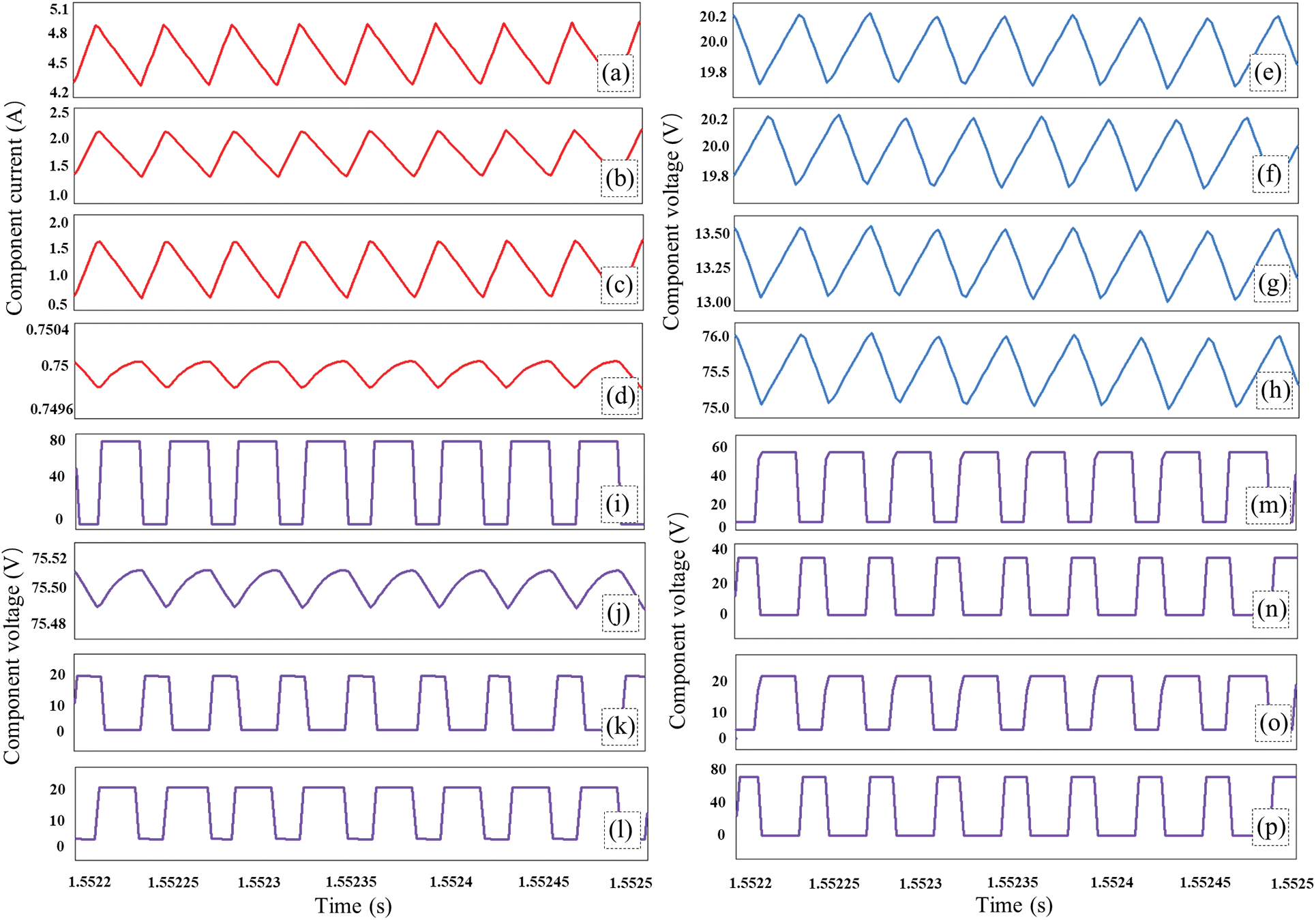
Figure 8: Simulation results: (a) current through the L1, (b) current through the L2, (c) current through the L3, (d) ouput current Io, (e) voltage across the C1, (f) voltage across the C2, (g) voltage across the C3, (h) voltage across the C4, (i) voltage across the S, (j) output voltage Vo (i.e., load voltage VR), (k) voltage of the D1, (l) voltage of the D2, (m) voltage of the D3, (n) voltage of the D4, (o) voltage of the D5, (p) voltage of the D6
In summary, the simulation analysis results confirm the validity of the theoretical analysis and demonstrate the excellent boost and device stress characteristics of the suggested converter.
The proposed converter employs the UC3842AN chip and peak current control (PCM) as its control strategy. Under this control strategy, dynamic simulation waveforms of the output voltage when input voltage jumps (Fig. 9a) are obtained, as shown in Fig. 9b. Additionally, dynamic simulation waveforms of the converter’s output voltage and output current during the transition from half to full load are acquired, as depicted in Figs. 9c and 9d, respectively. As demonstrated in Fig. 9b, when the input voltage changes in steps between 10 and 16 V, the output voltage undergoes dynamic responses. The overshoot of the output voltage is small, less than 0.8 V in both cases, and the adjustment time is short, less than 15 ms in both cases. Observations from Figs. 9c and 9d reveal that when output power jumps from half load, 28.5 W, to full load, 57 W, the output voltage experiences a small overshoot, approximately 1 V, while the adjustment time is approximately 16 ms. Subsequently, the output voltage stabilizes at around 75.5 V, and the output current stabilizes at around 0.75 A. These dynamic simulation results suggest that the proposed converter exhibits excellent dynamic performance.
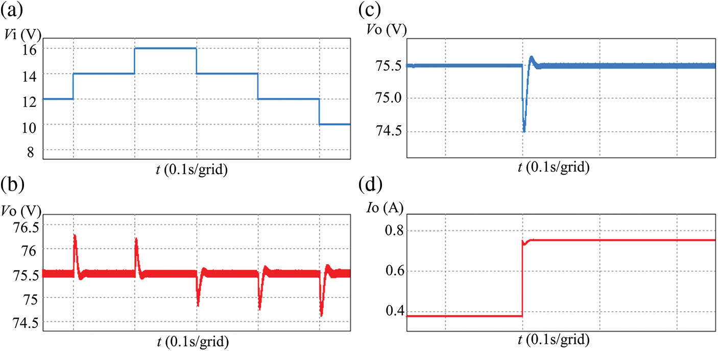
Figure 9: The dynamic simulation waveforms: (a) input voltage with a step change; (b) output voltage dynamic response; (c) output voltage in the transition from 28.5 to 57 W; (d) output current in the transition from 28.5 to 57 W
To further verify the accuracy and validity of the theoretical model, this study constructs an experimental prototype for testing. The prototype operates on an input voltage of 12 V, produces an output voltage of 75.5 V, and has a full load power of 57 W. Table 3 presents the key parameters of the experimental prototype. The values of capacitors and inductors in the experiment are consistent with the simulation, while also meeting the requirements of Eqs. (16) and (18), retaining a certain margin and considering performance and cost comprehensively. Then, device models are selected based on the values of capacitors and inductors. Fig. 10 showcases the physical appearance of the experimental prototype. Fig. 11 illustrates the experimental waveforms of the switch driving voltage VGS, power switch voltage VS, output voltage Vo (i.e., load voltage VR), capacitor C1 voltage VC1, diode D1 voltage VD1, diode D4 voltage VD4, inductor L1 current IL1, and output current Io at a duty cycle of 0.4.
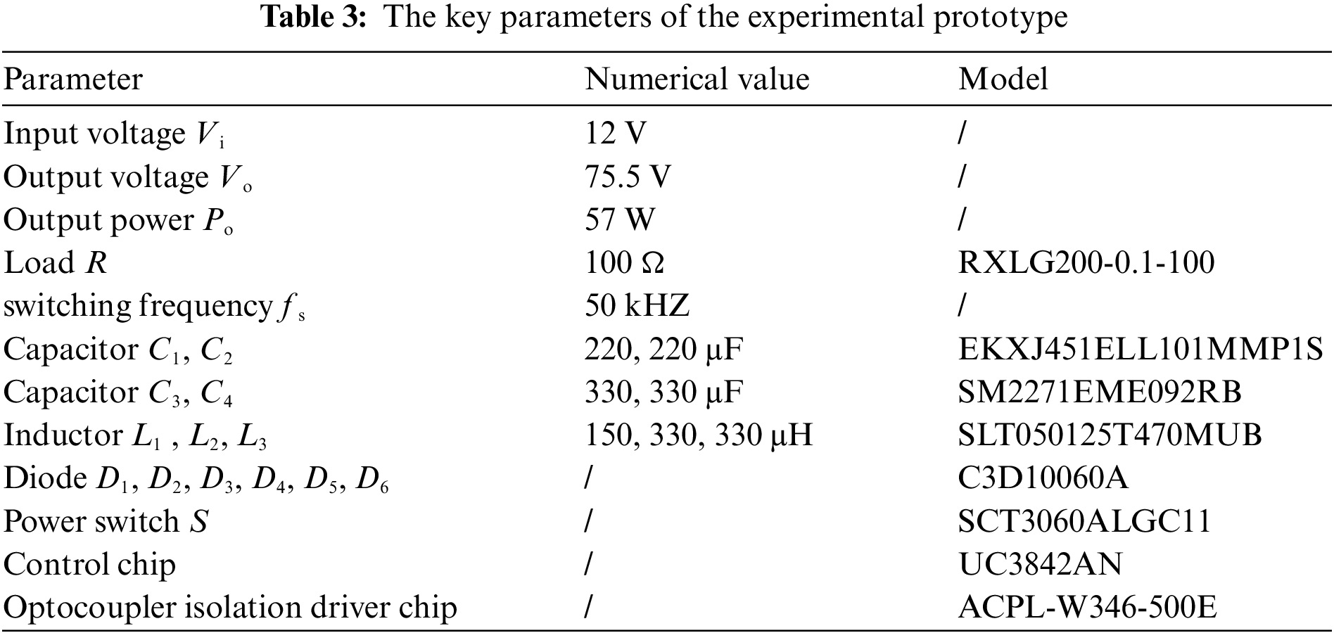
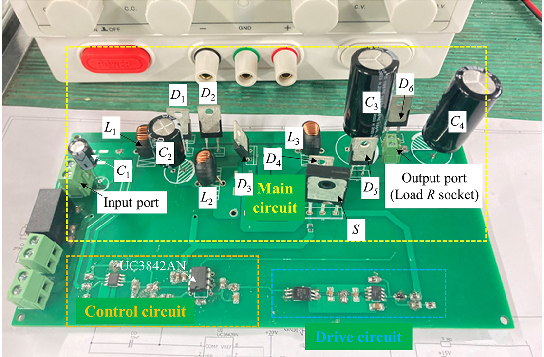
Figure 10: The physical appearance of the experimental prototype
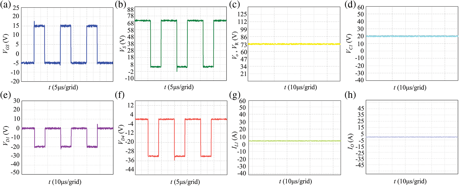
Figure 11: Experimental waveforms: (a) switching tube drive voltage VGS, (b) switching tube voltage VS, (c) output voltage Vo (i.e., load voltage VR), (d) capacitor C1 voltage VC1, (e) VD1 voltage across D1, (f) diode D4 voltage VD4, (g) inductor L1 current IL1, (h) output current Io
As depicted in Fig. 11a, the switch tube’s driving voltage VGS signal cycle is approximately 20 μs (frequency f = 50 kHz). The conduction drive voltage is 15 V, while the turn-off drive voltage is −5 V. The drive voltage signal meets the requirements of the SiC switch tube. Experimental results in Figs. 11b~11h are basically in agreement with theoretical calculation results. Nonetheless, the components are actually not ideal, and there are slight discrepancies between experimental and theoretical results. From Figs. 11c and 11h, the prototype’s output voltage Vo (i.e., load voltage) and output current Io are about 72.9 V and 0.72 A, respectively. However, the theoretical calculated values for Vo and Io are 75.5 V and 0.75 A, respectively. The experimental values for Vo and Io are lower by 3.44% and 4%, respectively, due to power loss of the devices. Fig. 11d illustrates that the capacitor voltage Vc1 is consistent with the theoretical value of 20 V. The capacitor voltage stress is relatively low. From Figs. 11e~11f, diode voltages VD1 and VD4 are approximately 19.8 and 32.2 V, respectively, consistent with theoretical calculation results. The experimental prototype has a higher voltage gain and lower device stress at a lower duty cycle. Table 4 presents a comprehensive comparison of the theoretical calculations, simulations, and experimental results for each parameter of the converter proposed in this paper. Table 4 indicates that the simulation and experimental results are largely consistent with the theoretical calculations, exhibiting minor errors, which affirms the accuracy of the theoretical analysis.
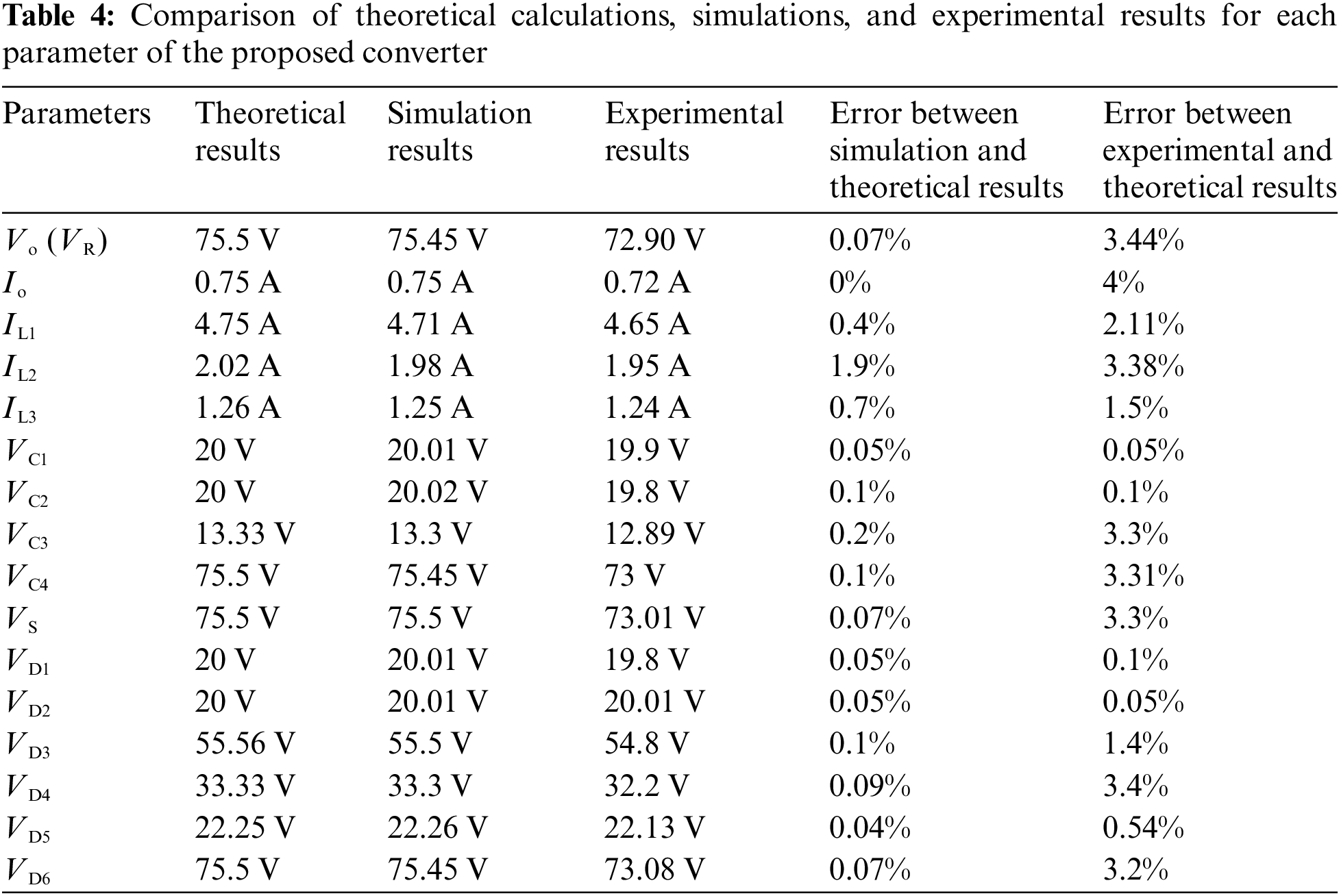
Fig. 12 illustrates the dynamic experimental waveform of the output voltage when the converter transitions from half load to full load. As indicated by Fig. 12, when the output power jumps from 28.5 to 57 W, the output voltage experiences a dynamic response, demonstrating a slight overshoot of approximately 2.1 V and a short adjustment time of approximately 18 ms. The experimental dynamic analysis results also attest to the proposed converter’s excellent dynamic performance.
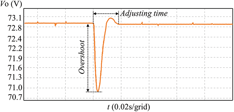
Figure 12: Output voltage dynamic experimental waveform
The power loss and conversion efficiency of the converter proposed in this paper are further analyzed. The theoretical efficiency and experimental efficiency of the converter are compared under varying duty ratios, as illustrated in Fig. 13a. While the experimental efficiency is slightly lower than the theoretical efficiency, the two measures remain generally close, exhibiting an error of less than 3%. This validates the accuracy of the theoretical calculation. Moreover, as the duty cycle increases, the theoretical and experimental efficiencies first increase and then decrease. Notably, when the duty ratio is 0.4, the power loss is found to be the smallest, and the theoretical and experimental efficiencies are the highest, reaching 93% and 91.9%, respectively. This observation confirms that the converter proposed in this study boasts high voltage gain and low device stress, while also achieving high conversion efficiency.
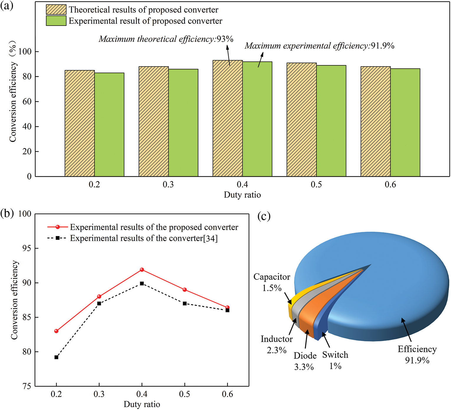
Figure 13: Power loss, conversion efficiency, and comparison: (a) the theoretical conversion efficiency and experimental efficiency of the proposed converter, (b) the experimental efficiency comparison, (c) the power loss distribution of the proposed converter
Furthermore, a comparison is made between the experimental efficiency of the proposed converter and that of a converter presented in a prior study [34], both under the same input voltage of 12 V, as illustrated in Fig. 13b. Although the efficiency of the proposed converter is almost identical to that of the converter [34] at a duty ratio of 0.6, the proposed converter exhibits a higher efficiency than the latter at duty ratios of 0.2, 0.3, 0.4, and 0.5, thus presenting a notable conversion efficiency advantage. Finally, Fig. 13c illustrates the power loss distribution of the proposed converter at a duty ratio of 0.4. The switch tube loss is the smallest, accounting for only 1% of the total loss. Meanwhile, the capacitor, inductor, and diode losses are found to account for 1.5%, 2.3%, and 3.3%, respectively. To further enhance the efficiency of the converter proposed in this work, high-quality circuit devices could be utilized.
This study introduces a novel non-isolated cubic high-gain DC-DC converter based on the traditional quadratic DC-DC boost converter by incorporating a SC and a SL-SC unit. Firstly, the proposed converter’s details are elaborated, including its topology structure, operating mode, voltage gain, device stress, and power loss. Subsequently, a comparative analysis is conducted on the voltage gain and device stress between the proposed converter and other high-gain converters. Then, a closed-loop simulation system is constructed to obtain simulation waveforms of various devices and explore the dynamic performance. Lastly, an experimental prototype is built, experimental waveforms are obtained, and the experimental dynamic performance and conversion efficiency are analyzed. The theoretical analysis’s correctness is verified through simulation and experimental results. The proposed converter achieves a high voltage gain at low device stress and high conversion efficiency, realizing a good balance between voltage gain, device stress, and power loss. The proposed converter is well-suited for renewable energy systems and holds theoretical significance and practical value in renewable energy applications. It offers a viable solution to the issue of low output voltage in renewable energy power generation systems. In future research, the emphasis will be placed on verifying the practical application effect of the proposed converter in renewable energy systems, exploring its working performance in various renewable energy systems such as new energy vehicles and photovoltaic power generation, and targeting improvements and optimizations to enhance its practicality.
Acknowledgement: The authors express their gratitude to the editor and anonymous reviewers for their reviews and valuable comments.
Funding Statement: This work was supported by China Railway Corporation Science and Technology Research and Development Project (P2021J038).
Author Contributions: The authors confirm their contribution to the paper as follows: Qin Yao: Conceptualization, Methodology, Simulation, Experiment, Drawing, Data processing, Writing-original draft, Writing-review & editing; Yida Zeng: Communication, Resources; Qingui Jia: Experimental support.
Availability of Data and Materials: Data supporting this study are included within the article.
Conflicts of Interest: The authors declare that they have no conflicts of interest to report regarding the present study.
References
1. Liang, T. J., Luo, P., Chen, K. H. (2021). A high step-up DC-DC converter with three-winding coupled inductor for sustainable energy systems. IEEE Transactions on Industrial Electronics, 69(10), 10249–10258. https://doi.org/10.1109/TIE.2021.3123683 [Google Scholar] [CrossRef]
2. Majeed, Y. E., Ahmad, I., Habibi, D. (2018). A multiple-input cascaded DC-DC converter for very small wind turbines. IEEE Transactions on Industrial Electronics, 66(6), 4414–4423. https://doi.org/10.1109/TIE.2018.2863214 [Google Scholar] [CrossRef]
3. Tan, K., Song, X., Peng, C., Liu, P., Huang, A. Q. (2016). Hierarchical protection architecture for 380V DC data center application. In 2016 IEEE Energy Conversion Congress and Exposition (ECCE), pp. 1–8. Milwaukee, WI, USA. https://doi.org/10.1109/ECCE.2016.7855145 [Google Scholar] [CrossRef]
4. Boroyevich, D., Cvetkovic, I., Burgos, R., Dong, D. (2013). Intergrid: A future electronic energy network? IEEE Journal of Emerging and Selected Topics in Power Electronics, 1(3), 127–138. https://doi.org/10.1109/JESTPE.2013.2276937 [Google Scholar] [CrossRef]
5. Ai, J., Lin, M., Yin, M. (2019). A family of high step-up cascade DC-DC converters with clamped circuits. IEEE Transactions on Power Electronics, 35(5), 4819–4834. https://doi.org/10.1109/TPEL.2019.2943502 [Google Scholar] [CrossRef]
6. Freitas, A. A. A., Tofoli, F. L., Sá Júnior, E. M., Daher, S., Antunes, F. L. M. (2015). High-voltage gain dc-dc boost converter with coupled inductors for photovoltaic systems. IET Power Electronics, 8(10), 1885–1892. https://doi.org/10.1049/iet-pel.2014.0520 [Google Scholar] [CrossRef]
7. Khalili, S., Esteki, M., Packnezhad, M., Farzanehfard, H., Khajehoddin, S. A. (2022). Fully soft-switched non-isolated high step-down DC-DC converter with reduced voltage stress and expanding capability. IEEE Journal of Emerging and Selected Topics in Power Electronics, 11(1), 796–805. https://doi.org/10.1109/JESTPE.2022.3180782 [Google Scholar] [CrossRef]
8. Hu, R., Zeng, J., Liu, J., Guo, Z., Yang, N. (2020). An ultrahigh step-up quadratic boost converter based on coupled-inductor. IEEE Transactions on Power Electronics, 35(12), 13200–13209. https://doi.org/10.1109/TPEL.2020.2995911 [Google Scholar] [CrossRef]
9. Maalandish, M., Hosseini, S. H., Ghasemzadeh, S., Babaei, E., Shalchi Alishah, R. (2017). Six-phase interleaved boost dc/dc converter with high-voltage gain and reduced voltage stress. IET Power Electronics, 10(14), 1904–1914. https://doi.org/10.1049/iet-pel.2016.1029 [Google Scholar] [CrossRef]
10. Saadat, P., Abbaszadeh, K. (2016). A single-switch high step-up DC-DC converter based on quadratic boost. IEEE Transactions on Industrial Electronics, 63(12), 7733–7742. https://doi.org/10.1109/TIE.2016.2590991 [Google Scholar] [CrossRef]
11. Izadi, M., Mosallanejad, A., Lahooti Eshkevari, A. (2023). A non-isolated quadratic boost converter with improved gain, high efficiency, and continuous input current. IET Power Electronics, 16(2), 193–208. https://doi.org/10.1049/pel2.12376 [Google Scholar] [CrossRef]
12. Hao, Y., Guo, K., Liu, L., Cai, W., Liu, F. (2022). Improved cubic boost converter based on voltage closed-loop control. Energy Reports, 8(4), 87–95. https://doi.org/10.1016/j.egyr.2022.03.069 [Google Scholar] [CrossRef]
13. Botila, D. A., Pop-Calimanu, I. M., Lascu, D. (2022). Cubic buck-boost converter with high step-up capability. In 2022 International Symposium on Electronics and Telecommunications (ISETC), pp. 1–4. Timisoara, Romania. https://doi.org/10.1109/ISETC56213.2022.10010074 [Google Scholar] [CrossRef]
14. Mahdizadeh, S., Alhashem, M. K., Kargar, H. K. (2022). A new cubic transformerless converter for applying in renewable applications. In 2022 13th Power Electronics, Drive Systems, and Technologies Conference (PEDSTC), pp. 515–519. Tehran, Iran. https://doi.org/10.1109/PEDSTC53976.2022.9767499 [Google Scholar] [CrossRef]
15. Zhang, N., Zhang, G., See, K. W., Zhang, B. (2017). A single-switch quadratic buck-boost converter with continuous input port current and continuous output port current. IEEE Transactions on Power Electronics, 33(5), 4157–4166. https://doi.org/10.1109/TPEL.2017.2717462 [Google Scholar] [CrossRef]
16. Gorji, S. A., Mostaan, A., Tran My, H., Ektesabi, M. (2019). Non-isolated buck-boost DC-DC converter with quadratic voltage gain ratio. IET Power Electronics, 12(6), 1425–1433. https://doi.org/10.1049/iet-pel.2018.5703 [Google Scholar] [CrossRef]
17. Gupta, N., Bhaskar, M. S., Almakhles, D., Sanjeevikumar, P., Subramaniam, U. (2020). Novel non-isolated quad-switched inductor double-switch converter for DC microgrid application. In 2020 IEEE International Conference on Environment and Electrical Engineering and 2020 IEEE Industrial and Commercial Power Systems Europe (EEEIC/I&CPS Europe), pp. 1–6. Madrid, Spain. https://doi.org/10.1109/EEEIC/ICPSEurope49358.2020.9160839 [Google Scholar] [CrossRef]
18. Wu, B., Li, S., Smedley, K. M., Singer, S. (2014). A family of two-switch boosting switched-capacitor converters. IEEE Transactions on Power Electronics, 30(10), 5413–5424. https://doi.org/10.1109/TPEL.2014.2375311 [Google Scholar] [CrossRef]
19. Banaei, M. R., Bonab, H. A. F. (2016). A novel structure for single-switch nonisolated transformerless buck-boost DC-DC converter. IEEE Transactions on Industrial Electronics, 64(1), 198–205. https://doi.org/10.1109/TIE.2016.2608321 [Google Scholar] [CrossRef]
20. Porselvi, T., Arounassalame, M. (2018). A novel single switch high gain DC-DC converter. 2018 8th IEEE India International Conference on Power Electronics (IICPE), pp. 1–6. Jaipur, India. https://doi.org/10.1109/IICPE.2018.8709508 [Google Scholar] [CrossRef]
21. Naresh, S. V. K., Peddapati, S. (2021). New family of transformer-less quadratic buck-boost converters with wide conversion ratio. International Transactions on Electrical Energy Systems, 31(11), e13061. https://doi.org/10.1002/2050-7038.13061 [Google Scholar] [CrossRef]
22. Ahmad, S., Nasir, M., Dąbrowski, J., Guerrero, J. M. (2021). Improved topology of high voltage gain DC-DC converter with boost stages. International Journal of Electronics Letters, 9(3), 342–354. https://doi.org/10.1080/21681724.2020.1744040 [Google Scholar] [CrossRef]
23. Tewari, N., Sreedevi, V. T. (2018). A novel single switch DC-DC converter with high voltage gain capability for solar PV based power generation systems. Solar Energy, 171, 466–477. https://doi.org/10.1016/j.solener.2018.06.081 [Google Scholar] [CrossRef]
24. Li, G., Jin, X., Chen, X., Mu, X. (2020). A novel quadratic boost converter with low inductor currents. CPSS Transactions on Power Electronics and Applications, 5(1), 1–10. https://doi.org/10.24295/CPSSTPEA.2020.00001 [Google Scholar] [CrossRef]
25. Naresh, S. V. K., Peddapati, S., Alghaythi, M. L. (2021). Non-isolated high gain quadratic boost converter based on inductor’s asymmetric input voltage. IEEE Access, 9, 162108–162121. https://doi.org/10.1109/ACCESS.2021.3133581 [Google Scholar] [CrossRef]
26. Rahimi, T., Ding, L., Gholizadeh, H., Shahrivar, R. S., Faraji, R. (2021). An ultra high step-up DC-DC converter based on the boost, Luo, and voltage doubler structure: Mathematical expression, simulation, and experimental. IEEE Access, 9, 132011–132024. https://doi.org/10.1109/ACCESS.2021.3115259 [Google Scholar] [CrossRef]
27. Chen, J., Ding, K., Zhong, Y., Deng, F., Abulanwar, S. (2020). A double input-parallel-output-series hybrid switched-capacitor boost converter. Chinese Journal of Electrical Engineering, 6(4), 15–27. https://doi.org/10.23919/CJEE.2020.000027 [Google Scholar] [CrossRef]
28. Maalandish, M., Hosseini, S. H., Jalilzadeh, T. (2018). High step-up DC/DC converter using switch-capacitor techniques and lower losses for renewable energy applications. IET Power Electronics, 11(10), 1718–1729. https://doi.org/10.1049/iet-pel.2017.0752 [Google Scholar] [CrossRef]
29. Tekin, H., Bulut, K., Ertekin, D. (2022). A novel switched-capacitor and fuzzy logic-based quadratic boost converter with mitigated voltage stress, applicable for DC micro-grid. Electrical Engineering, 104, 1–23. https://doi.org/10.1007/s00202-022-01631-3 [Google Scholar] [CrossRef]
30. Sadaf, S., Bhaskar, M. S., Meraj, M., Iqbal, A., Al-Emadi, N. (2020). A novel modified switched inductor boost converter with reduced switch voltage stress. IEEE Transactions on Industrial Electronics, 68(2), 1275–1289. https://doi.org/10.1109/TIE.2020.2970648 [Google Scholar] [CrossRef]
31. Stala, R., Waradzyn, Z., Folmer, S. (2022). Input current ripple reduction in a step-up DC-DC switched-capacitor switched-inductor converter. IEEE Access, 10, 19890–19904. https://doi.org/10.1109/ACCESS.2022.3152543 [Google Scholar] [CrossRef]
32. Tang, Y., Wang, T., Fu, D. (2014). Multicell switched-inductor/switched-capacitor combined active-network converters. IEEE Transactions on Power Electronics, 30(4), 2063–2072. https://doi.org/10.1109/TPEL.2014.2325052 [Google Scholar] [CrossRef]
33. Kumar, A., Wang, Y., Pan, X., Raghuram, M., Singh, S. K. et al. (2020). Switched-LC based high gain converter with lower component count. IEEE Transactions on Industry Applications, 56(3), 2816–2827. https://doi.org/10.1109/TIA.2020.2980215 [Google Scholar] [CrossRef]
34. Subhani, N., May, Z., Alam, M. K., Khan, I., Hossain, M. A. et al. (2023). An improved non-isolated quadratic DC-DC boost converter with ultra high gain ability. IEEE Access, 11, 11350–11363. https://doi.org/10.1109/ACCESS.2023.3241863 [Google Scholar] [CrossRef]
Cite This Article
 Copyright © 2024 The Author(s). Published by Tech Science Press.
This work is licensed under a Creative Commons Attribution 4.0 International License , which permits unrestricted use, distribution, and reproduction in any medium, provided the original work is properly cited.
 Downloads
 Citation Tools