
 Login
Login Register
 Submit a Paper
 Propose a Special lssue
 Open Access
ARTICLE
MMC Submodule Topology for Integrated Photovoltaic and Energy Storage Converters and Its Double-Layer Balance Control Strategy
Economic and Technical Research Institute of State Grid Sichuan Electric Power Company, Chengdu 610000, China
* Corresponding Author: Fan Shao. Email:
(This article belongs to the Special Issue: Operation and Control of Grid-connected New Energy and Emerging Loads)
Energy Engineering 2026, 123(11), 13 https://doi.org/10.32604/ee.2025.072469
Received 27 August 2025; Accepted 10 November 2025; Issue published 24 September 2026
 View Full Text
 Download PDF
Abstract
The rapid growth of distributed photovoltaic (PV) power generation has led to higher requirements for reliable and efficient photovoltaic-storage integrated converters. Traditional half bridge sub-module structures face significant challenges, including limited DC fault-blocking capability and uneven loss distribution among sub-modules due to variations in the conduction characteristics of power devices. To address these issues, this study proposes innovations in both topology and control strategy. A clamp double energy storage submodule (CDESSM) with inherent fault self-blocking capability is designed, improving system safety under fault conditions. Furthermore, a nearest level modulation (NLM) algorithm based on conduction time equalization is developed, combined with a dual-layer sub-module capacitor voltage balancing scheme to maintain uniform voltage distribution across sub-modules. The proposed design effectively reduces voltage deviation, balances losses, and enhances overall converter performance. Simulation demonstrates that the improved system maintains stable output under normal operating conditions and can isolate DC faults within milliseconds, validating its reliability. RT-LAB testing further confirms the engineering feasibility of the proposed topology and control strategy, indicating its potential for practical applications in PV-storage integrated systems. The combination of structural innovation and advanced control methods provides a promising approach for enhancing the performance, safety, and longevity of next generation PV-storage converters.Keywords
In recent years, the development of clean energy has gained increasing attention. Among them, solar power generation technology has occupied a significant position in the field of distributed energy due to its economic efficiency and environmental friendliness [1,2]. However, this technology has inherent defects such as large output fluctuations and uncontrollability, which restrict its large-scale development. To address this technical bottleneck, the photovoltaic (PV) and energy storage collaborative system has emerged, becoming a key technical solution to maintain the stable operation of the power grid [3,4].
As the core component of this system, traditional two-level converters exhibit significant limitations when applied to large-capacity, high-voltage scenarios [5–7]. The multi-module cascading approach not only increases harmonic distortion and reduces efficiency but also introduces the risk of system failure due to single-point faults, thereby compromising power supply reliability. In contrast, the Modular Multilevel Converter (MMC) offers an effective solution for photovoltaic-storage systems, thanks to its superior output waveform quality, high efficiency, and modular architecture. Its unique submodule design supports redundancy and enables distributed integration of energy storage units, substantially reducing the voltage and capacity requirements for individual batteries [8–10].
Research on MMC has made progress in multiple aspects. In terms of topological structures, scholars have proposed different technical schemes: Reference [11] designed a bidirectional switch diode-clamped submodule, which can effectively clear DC faults. However, the increase in the number of nonlinear devices leads to a decline in the steady-state operation performance of the system. The clamp double energy storage submodule structures studied in References [12,13] have prominent economy and simple structures, but suffer from insufficient fault isolation response speed. In the field of control strategies, References [14,15] improved the traditional voltage balancing algorithm, significantly enhancing calculation efficiency, but the program implementation is relatively complex. Reference [16] applied the NLC-SHE hybrid modulation strategy to improve harmonic characteristics, but this offline algorithm struggles to adapt to the fluctuating characteristics of new energy power generation. Aiming at DC fault issues, References [17–19] studied the half-full bridge hybrid sub-module topology and determined the optimal configuration ratio of full-bridge sub-modules. The virtual impedance method proposed in Reference [20,21] has adaptive adjustment capabilities, enabling simultaneous control of fault current and arm current, but requires additional current limiting devices, increasing system costs. Research on coordinated PV–ES scheduling [22,23] has focused on optimizing multi-energy interactions and improving energy utilization efficiency in distributed systems. Existing studies show that the MMC topologies suitable for photovoltaic-storage systems are limited, control methods are difficult to match the characteristics of new energy power generation, and the DC fault suppression effect needs improvement.
This study focuses on the topological characteristics of the clamp double energy storage submodule, innovatively combining nearest level modulation (NLM) with double-layer capacitor voltage balancing control. By establishing a complete control system, it realizes dynamic balance of capacitor voltage and rapid isolation of DC faults, providing new ideas for the optimization of photovoltaic-storage integrated converters. Simulation and experimental results show that the proposed control strategy has good engineering application value.
In summary, although various MMC-based converter topologies and control strategies have been reported in recent years, most of them either focus on improving fault blocking capability [11–13] or enhancing voltage balancing performance [14–16], but few studies integrate both aspects in a unified framework suitable for photovoltaic–storage systems. To address these gaps, this work makes the following key contributions:
(1) A novel clamp double energy storage submodule (CDESSM) is proposed, featuring an intrinsic fault self-blocking mechanism. Compared with conventional half-bridge and diode-clamped structures [11–13], the CDESSM effectively suppresses DC-side fault currents without relying on external current-limiting devices.
(2) A conduction-time-equalized nearest level modulation (NLM) scheme is developed to ensure uniform loss distribution among power devices, overcoming the uneven switching losses commonly observed in conventional NLM-based MMCs [14,15].
(3) An internal–external double-layer capacitor voltage balancing control strategy is designed, which achieves fast voltage equalization between submodules and capacitors, enhancing overall system stability under dynamic photovoltaic and storage conditions.
The proposed topology and control framework are comprehensively validated through both detailed simulations and real-time RT-LAB experiments, demonstrating strong potential for scalable application in next-generation photovoltaic–energy storage integrated converters.
2 Structure and Mathematical Model of Photovoltaic-Storage Integration System
2.1 Overall Structure of Photovoltaic-Storage Integration System
Fig. 1a presents the overall architecture of the photovoltaic-storage integration system. The key component of this system is the MMC-based photovoltaic-storage power conversion device, whose main function is to regulate the direction of energy flow within the system. Structurally, the conversion device includes six power arms in three phases, while integrating a photovoltaic cell array PV and a parallel DC filter capacitor. Each power arm adopts a modular design, consisting of several Energy Storage Submodules (ESSMs) connected in series with an inductive component Larm.
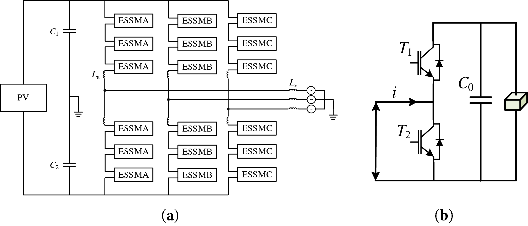
Figure 1: The topology of MMC. (a) Topology of MMC-type Integrated PV and ES converter. (b) Topology of the ESSM
Fig. 2 illustrates the specific circuit design of the improved energy storage unit clamp double energy storage submodule (CDESSM), which aims to address the inherent defects of the traditional half-bridge structure. The traditional ESSM adopts the half-bridge architecture shown in Fig. 1b, comprising a pair of IGBT switching tubes (T1, T2), parallel diodes (D1, D2), a support capacitor, and a battery pack. This design has obvious limitations: due to the effect of the freewheeling diodes, it is difficult to quickly cut off the current when a short-circuit fault occurs in the DC side, thus threatening the operational stability of the system. In contrast, the newly proposed clamp double energy storage submodule effectively overcomes this technical bottleneck through innovative topology optimization.
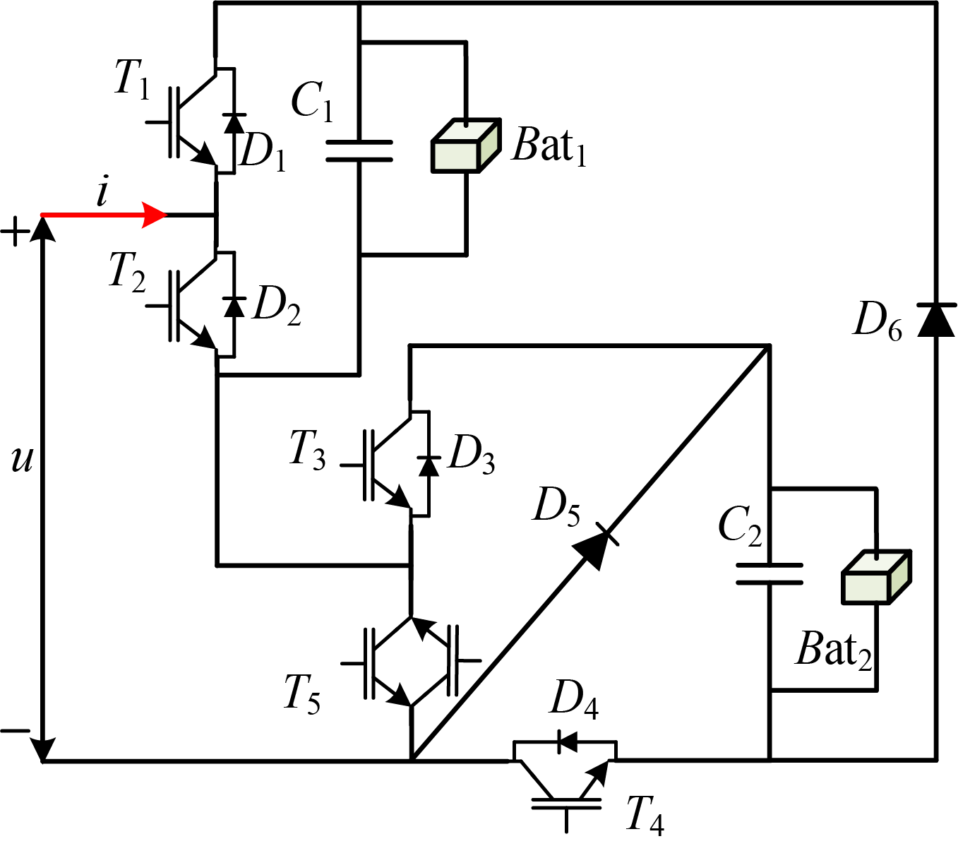
Figure 2: The topology of CDESSM
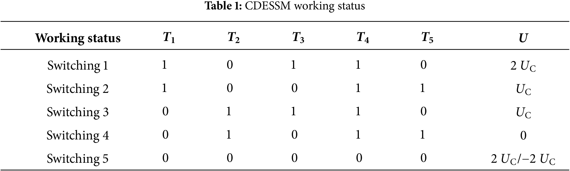
CDESSM adopts a multi-device composite structure, including four groups of IGBT switches (T1–T4), corresponding anti-parallel diodes (D1–D4), RB-IGBT with reverse blocking capability (T5), parallel capacitor banks (C1, C2), and dual battery configurations (Bat1, Bat2). By controlling the conduction combination of power switching tubes, the circuit produces three discrete voltage levels, which corresponding to the submodule switching states: 0, single-capacitor voltage (UC), and dual-capacitor voltage (2 UC). 2 UC represents the terminal voltage when the arm current flows in the forward direction, and −2 UC represents the terminal voltage when the current flows in the reverse direction. The specific operation modes can be divided into four typical working conditions, and the detailed parameter correspondence is shown in Table 1.
2.3 Mathematical Model of Photovoltaic-Storage Integration System Converter
Existing studies have established a relatively complete mathematical description system for MMC. Based on this theoretical foundation, this section focuses on deriving the mathematical characterization of CDESSM and its operation mechanism. With reference to the circuit parameter definitions shown in Fig. 1, the current characteristics of the topology’s AC side can be fully described by Eqs. (1)–(4).
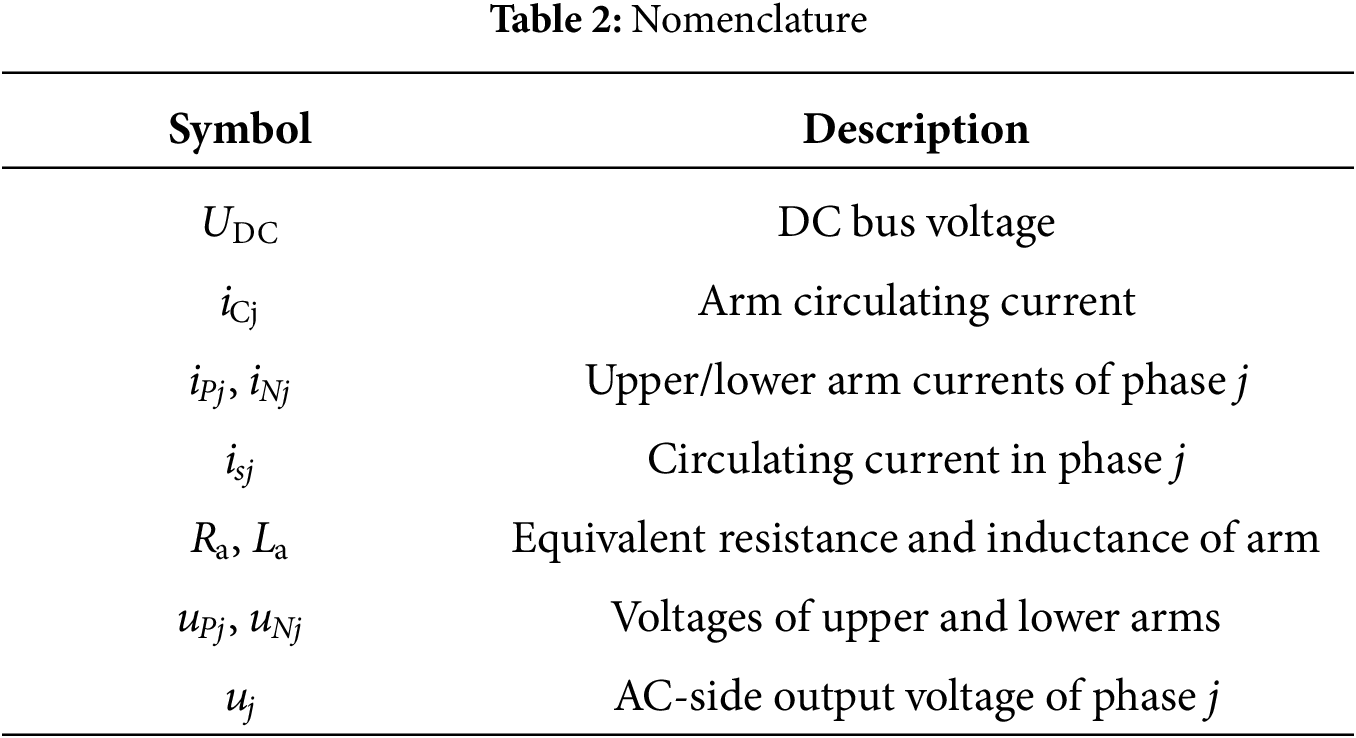
Among them, IDC represents the DC-side current component, iCj represents the arm circulating current, and isj corresponds to the current of the j-phase AC port. During the operation of the converter, the currents of the upper and lower arms are recorded as iPj and iNj, respectively. The arm circulating current izj, as a current component, transfers active power between the upper and lower arms to ensure that the voltage of each arm remains dynamically balanced.
Regarding the voltage characteristics of CDESSM, the mathematical constraint relationship between the arm output voltage and the AC-side voltage is as follows:
Among them, Ra represents the arm equivalent impedance parameter, and UDC is the DC bus voltage. In the working state of phase j, the output voltage of the converter’s AC side is denoted as uj, while the voltages of the upper and lower arms are expressed as uPj and uNj, respectively.
By performing addition and subtraction operations on Eqs. (5) and (6), it can be derived that:
Analysis of the above mathematical expressions shows that under normal operating conditions, the working mechanism of CDESSM is highly consistent with that of the traditional MMC. However, when a short-circuit anomaly occurs in the DC side, the traditional structure struggles to achieve fault ride-through capability. Aiming at this critical issue, based on the unique circuit architecture of CDESSM, an effective fault blocking strategy must be designed to reliably cut off the fault current path. Table 2 presents the Nomenclature table for the a forementioned mathematical analysis.
DC-side faults that may occur in flexible DC transmission systems mainly include three types: bipolar short circuit, monopolar grounding, and DC disconnection. Among them, bipolar short-circuit faults pose the most serious threat to system operation. Based on this consideration, this study selects the bipolar short-circuit condition as a typical case to deeply discuss the dynamic response and blocking mechanism of CDESSM under fault conditions. Fig. 3 shows the current path distribution of this topology in the locked state.
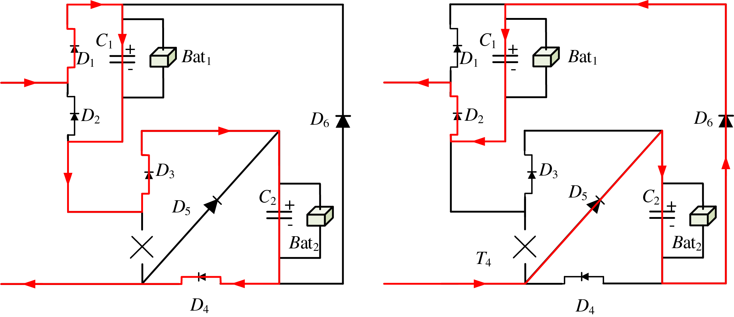
Figure 3: Fault current flow path
When a fault is detected, all submodule IGBTs in the converter are blocked. When the fault current flows forward into the submodule, the current passes through diodes D1, D3, and D4, charging capacitors C1 and C2 in the circuit. The charged capacitors generate a reverse electromotive force (EMF) that suppresses the fault current. Conversely, when the fault current flows in the reverse direction, it conducts through diodes D2, D5, and D6, charging the same capacitors C1 and C2, which again provide a reverse EMF to interrupt the fault current. It is noteworthy that, regardless of the current direction, the submodule is electrically equivalent to two series-connected capacitors, supplying twice the EMF to block the fault current, as illustrated in Fig. 3.
During the continuous operation of the CDESSM system, the DC bus status is continuously detected by the real-time monitoring device. When a short-circuit fault is identified, the control unit immediately issues a blocking command to make all IGBTs enter the blocking state to cut off the fault path. For transient faults, the system automatically releases the blocking after the current is blocked, and reactivates the power devices to restore the DC voltage establishment process; for permanent faults, it maintains the IGBT trigger pulse blocking state, and at the same time disconnects the AC side circuit breaker to achieve the safe isolation of the converter device and the power grid. The complete fault handling logic is shown in the control flow chart of Fig. 4.
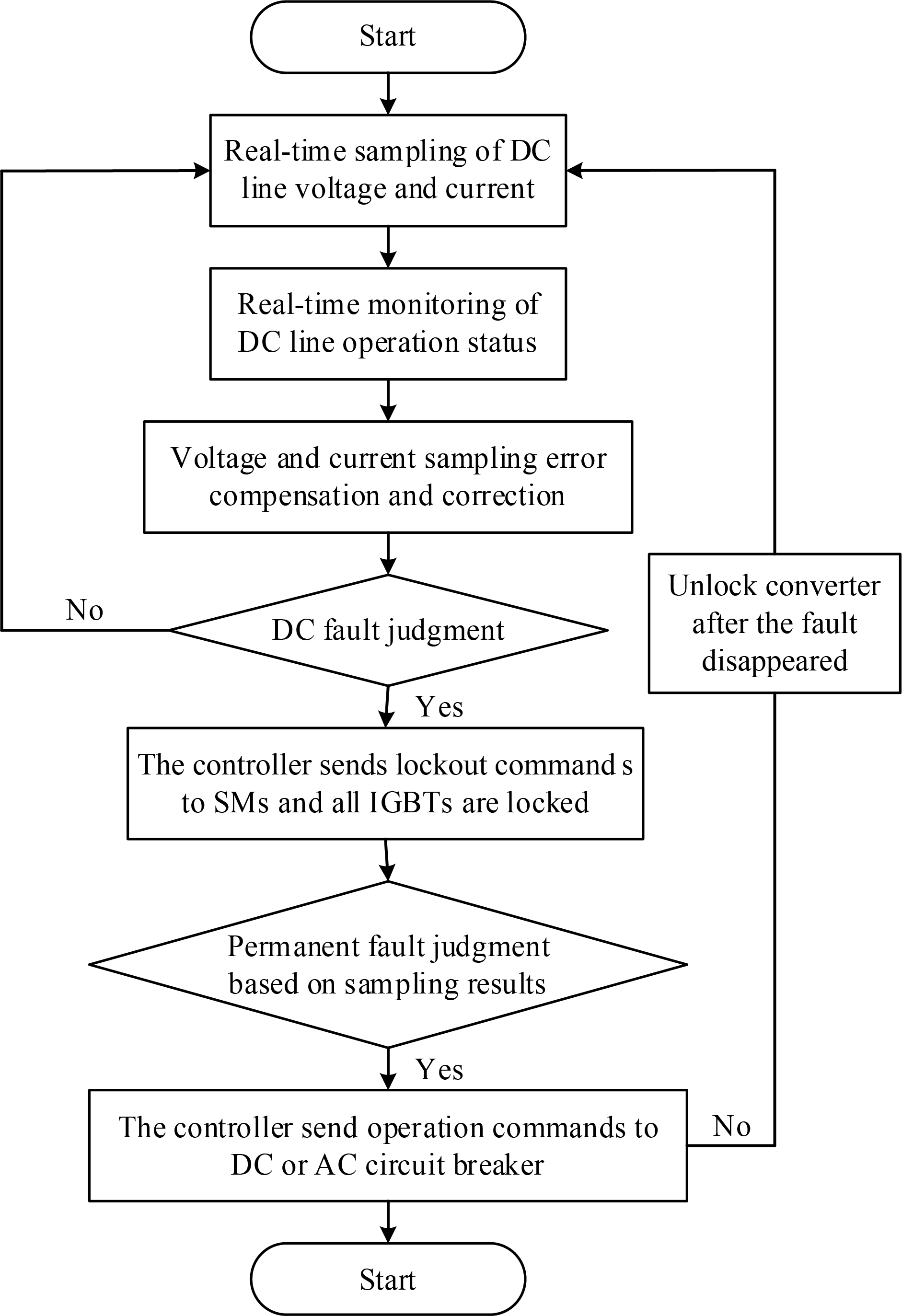
Figure 4: Control flow chart of DC fault
4 Control Strategy of Photovoltaic-Storage Integration System Converter
Based on the traditional nearest level modulation principle, this section proposes an improved NLM control scheme to adapt to the special working characteristics of CDESSM. Considering that this topology has dual-level output capability, a time-division conduction technology is adopted. By accurately allocating the conduction periods of each device, the unbalanced loss caused by differences in switching probability is improved. Furthermore, combined with this time-division modulation method, a new capacitor voltage balancing control system is developed. Using an internal and external double-layer regulation architecture, it realizes more precise voltage equalization management.
4.1 NLM Strategy for Time-Equally-Conducted CDESSM
Aiming at the modular architecture of CDESSM, take the a-phase circuit shown in Fig. 1 as an example for analysis. This phase includes two symmetric arms, each arm contains N energy storage modules, and each module is equipped with two capacitor elements, so the total number of capacitors n = 2 N. During system operation, each phase always keeps n capacitors in working state. In the balanced working condition, when the number of capacitors in the upper and lower arms is equal, the phase voltage output is zero, as shown in Fig. 5. With the dynamic adjustment of the modulation signal, the number of capacitors invested in the arm changes accordingly, so as to achieve the precise tracking of the output voltage to the modulation wave.
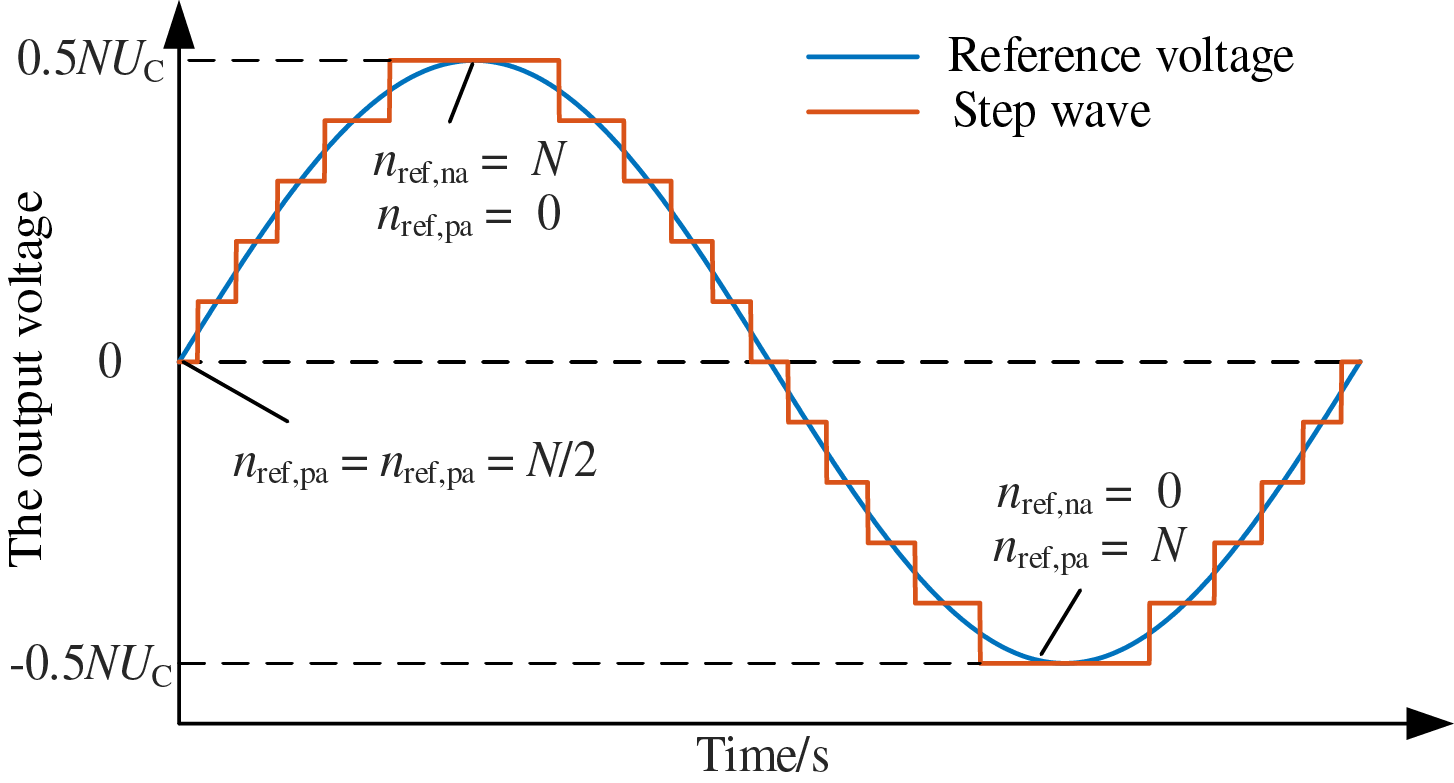
Figure 5: Principle of nearest level modulation
The number of capacitors required to be invested in the upper and lower arms at any time can be determined by the following formula:
This expression uses the round(x) function to implement numerical rounding operations, where Udc represents the amplitude of the DC bus voltage, m denotes the modulation ratio, and φ is the phase angle of the current phase modulation signal.
At a certain moment, it is assumed that the upper arm of phase a needs to invest K energy storage modules. Considering that CDESSM has the capability to output three levels of 0, UC, and 2 UC, which is fundamentally different from the traditional half-bridge structure, the simple input/resect control mode is no longer applicable. To address this issue, this study adopts a grouping modulation method, dividing the sub-modules into three working states: the first type outputs 2 UC, the second type generates UC, and the third type maintains zero-level output. Let the quantities of these three types of modules be K1, K2, and K3, and their mathematical relationships can be expressed as:
Among them, K1 is the integer part of K divided by two, K2 corresponds to the remainder of K divided by two, and K3 represents the number of remaining modules not put into operation.
To achieve the balanced operation of Switching 2 and Switching 3 listed in Table 1, a time-division scheme is designed: the working cycle of the second-type modules is divided into two equal periods. The first half-period is provided with UC level by Switching 2, and the second half-period is switched to Switching 3. This alternating working mode significantly improves the loss distribution characteristics among power devices.
4.2 Internal and External Double-Layer Balance Control Strategy for CDESSM Capacitor Voltage
Aiming at the three-level output characteristics of CDESSM, the working state allocation of sub-modules requires a special control strategy. After obtaining the required number of capacitors through modulation wave setting, differentiated processing should be adopted according to the parity of the value. The voltage balancing control architecture shown in Fig. 6 uses a sorting algorithm to dynamically select the sub-modules put into operation and their internal capacitor configurations.
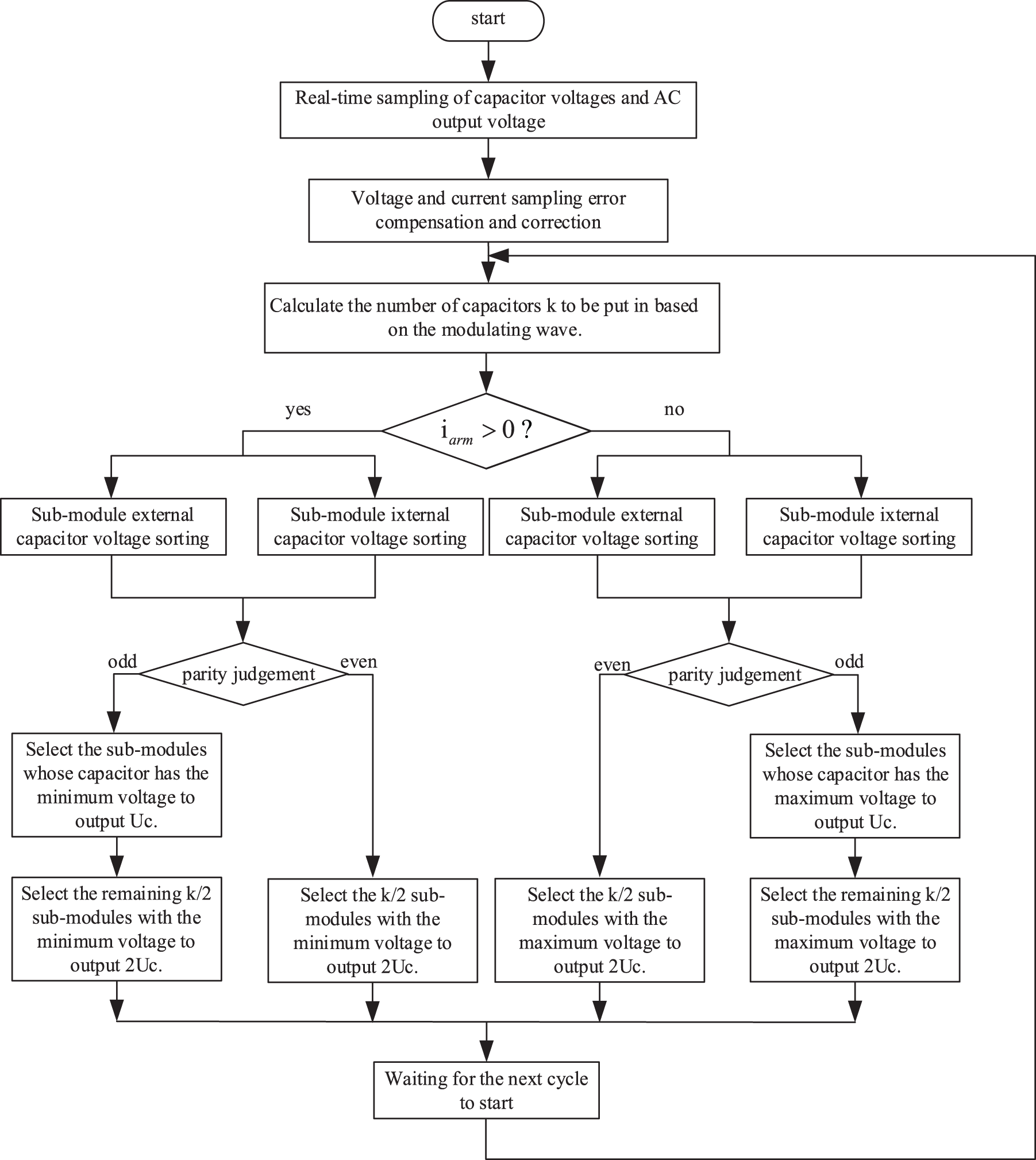
Figure 6: Double-layer equalization control strategy of internal and external capacitor voltage of SM
The specific implementation process is as follows: it is assumed that after time-division modulation, the upper arm of phase a needs to invest k capacitors, and the arm current iarm is greater than 0. The system first sorts and detects the internal and external capacitor voltages of all sub-modules. When k is odd, select k/2 sub-modules with the lowest voltage to output 2 UC, and specify a module with the lowest internal capacitor voltage to output UC, while the rest remain in a zero state. If k is even, only k/2 sub-modules are required to output 2 UC. At the beginning of each control cycle, the system re-executes the dynamic selection process to ensure voltage balance and uniform loss distribution.
5 Simulation and Experimental Verification
5.1 System Steady-State Operation Simulation
This section verifies the steady-state performance of the CDESSM system through simulation experiments, adopting the improved time-division NLM modulation method and the dual-layer capacitor voltage balancing control scheme. A 0.2-s simulation test is conducted under a single-terminal system architecture, and the obtained steady-state operation characteristics are shown in Figs. 7–9, fully presenting the dynamic waveforms of key electrical parameters.
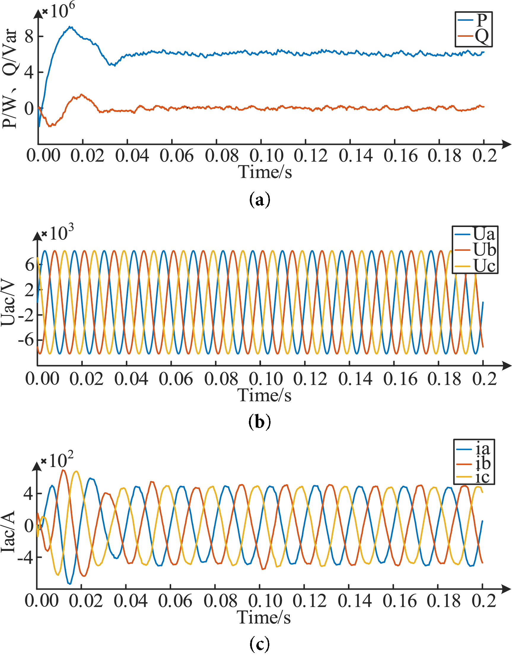
Figure 7: Waveform of steady-state running. (a) Waveform of active and reactive power. (b) Waveform of AC side voltage. (c) Waveform of AC side current
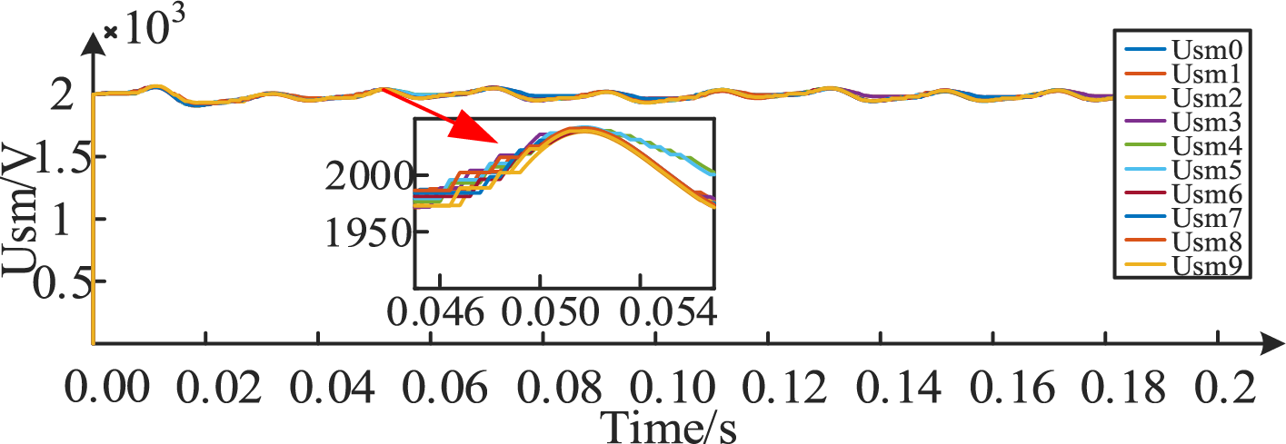
Figure 8: SM voltage waveform of upper bridge arm of phase A
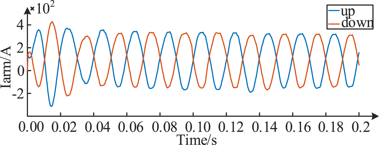
Figure 9: Arm current of bridge A
Fig. 7a illustrates the dynamic response process of the system’s power characteristics, where the reference value of active power on the AC side is set to 6 mw, and the reactive power maintains zero output. From the waveform, it can be observed that after a 30 ms adjustment process, the actual power value converges to the vicinity of the command value, with the active power tracking error controlled within 6%, achieving a stable operation state. Fig. 7b,c presents the voltage and current characteristics of the AC port: the voltage exhibits a standard 50 Hz/10 kV three-phase sine waveform, while the current shows transient fluctuations at the initial startup stage and stabilizes at an effective value of 350 A after a 30 ms transition period.
Figs. 8 and 9 detail the dynamic operation process of the sub-modules. When the arm current is in the positive direction, the capacitor is in a charging state, and the voltage gradually rises; when the current reverses, it switches to a discharging mode, and the voltage decreases accordingly. This periodic charging and discharging keep the capacitor voltage fluctuating around the 2 kV reference value. The measured maximum value is 2.052 kV, the minimum value is 1.942 kV, and the voltage ripple amplitude is 5.5%, verifying the effectiveness of the proposed voltage balancing strategy. The voltages of each sub-module maintain good consistency, and the system operation state meets the design requirements.
5.2 Comparison between the Proposed Method and Traditional Method
This section compares the proposed method with existing methods in terms of total harmonic distortion rate, loss characteristics, and capacitor voltage ripple characteristics during steady-state operation of MMC. Figs. 10 and 11 compared the harmonic distortion of the upper/lower arm currents and AC output current under the conventional nearest level modulation (NLM) method and the proposed conduction-time-equalized control strategy. The results, shown in Figs. 10 and 11, indicate that the THD values remain almost unchanged between the two methods. Since the arm current inherently contains a large DC component, the THD values are 24.45% and 24.37%, respectively.
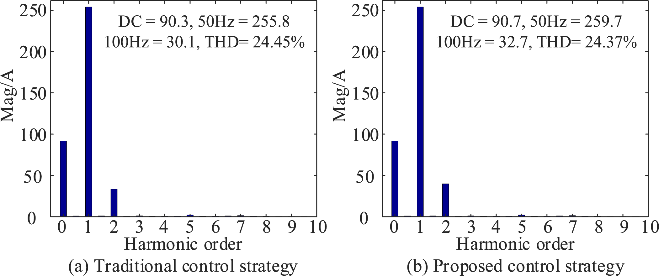
Figure 10: Bridge arm current thd analysis for traditional methods and the proposed method
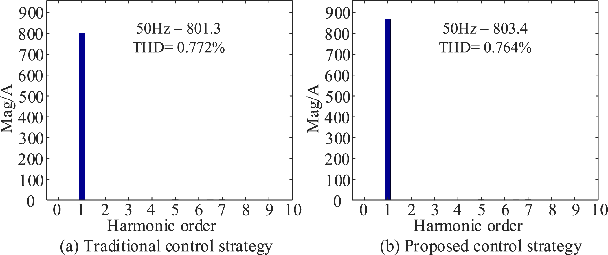
Figure 11: AC THD analysis of traditional methods and the proposed method in this paper
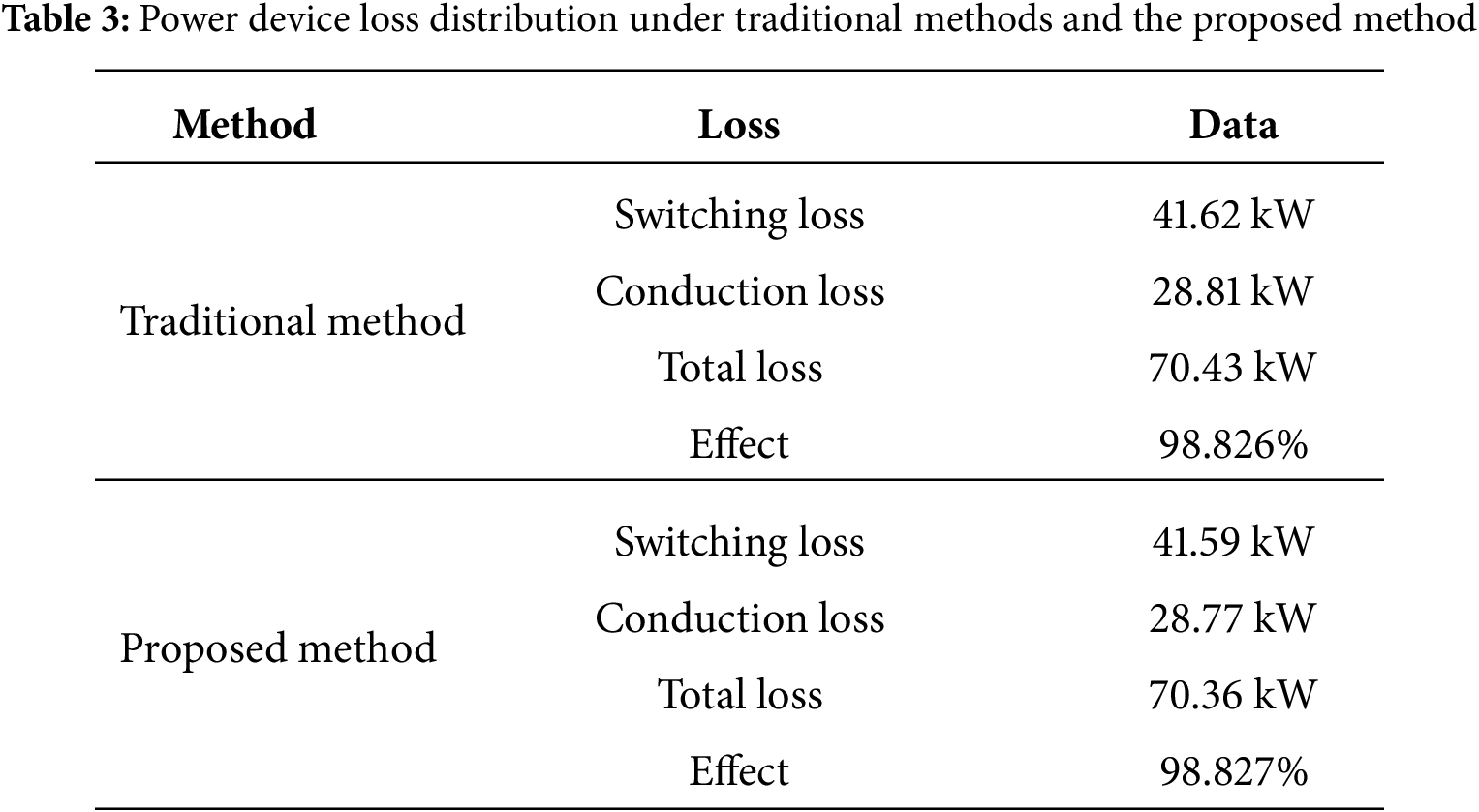
Referring to the converter loss calculation method in Reference [24], the total semiconductor loss and overall converter efficiency under both modulation schemes are evaluated. The quantitative results are summarized in Fig. 12 and Table 3. It can be observed that the total converter loss and efficiency under the two methods are nearly identical, confirming that the proposed control strategy does not introduce additional losses.
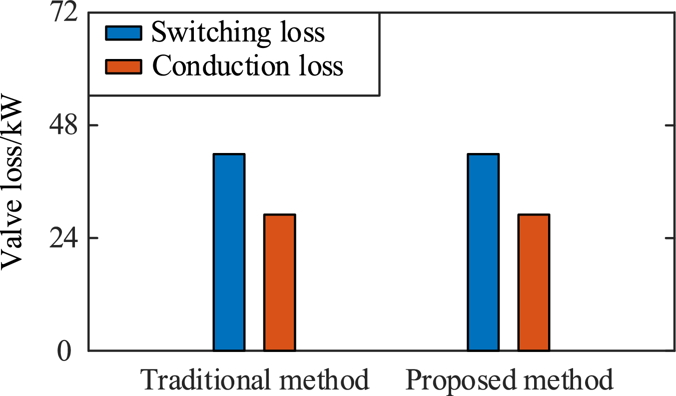
Figure 12: Power device loss distribution under traditional methods and the proposed method
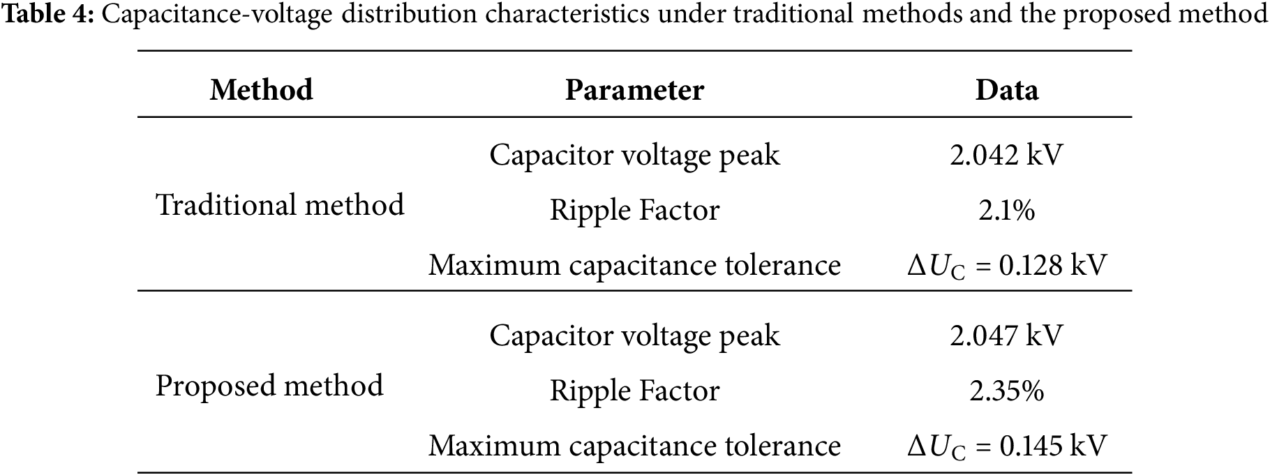
The capacitor voltage waveforms under the two modulation methods are shown in Fig. 13, with data comparisons presented in Table 4. For the conventional method, the peak capacitor voltage is 2.042 kV with a ripple factor of 2.1%, and the maximum voltage deviation is ΔUC = 0.128 kV. Under the proposed method, the peak voltage is 2.047 kV, the ripple factor is 2.35%, and ΔUC = 0.145 kV. The results show that the capacitor voltage ripple characteristics of the proposed control method are consistent with those of the conventional scheme.
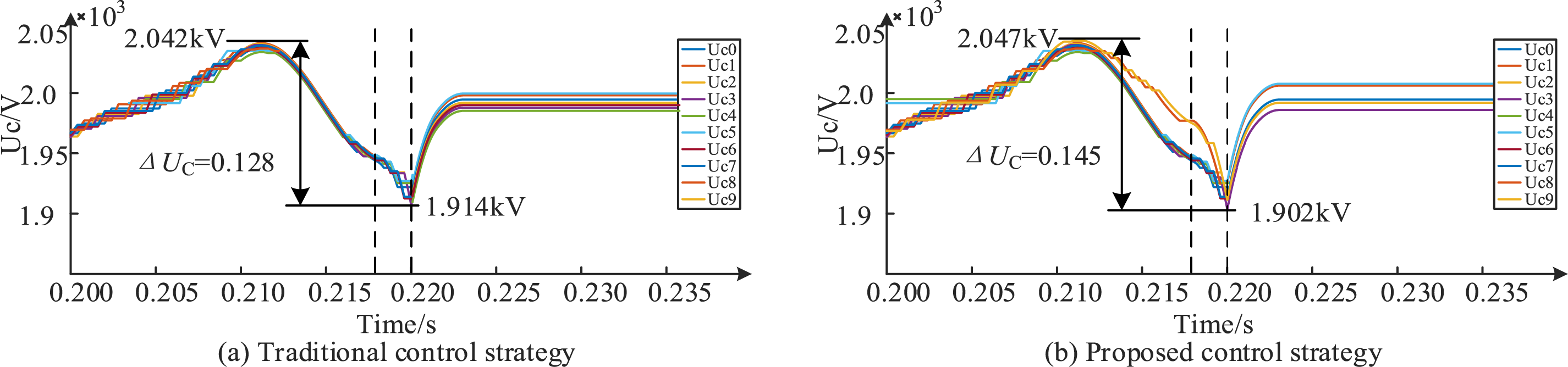
Figure 13: Capacitance-voltage distribution characteristics under traditional methods and the proposed method
5.3 System Fault Condition Simulation
To verify the system’s fault protection performance, this section focuses on simulating the severe fault condition of DC bipolar short circuit. The simulation sets the system to maintain stable operation in the interval of 0–0.218 s, and a permanent bipolar short-circuit fault signal on the DC side is artificially injected at 0.218 s. After a detection delay of 2 ms, the control system successfully blocks all IGBT trigger signals at 0.22 s. The waveform diagrams in Figs. 14 and 15 clearly show the dynamic changes of key parameters during the fault, including the characteristics of DC bus voltage and current, the voltage fluctuation of energy storage module capacitors, and the electrical quantity response process of the AC port.
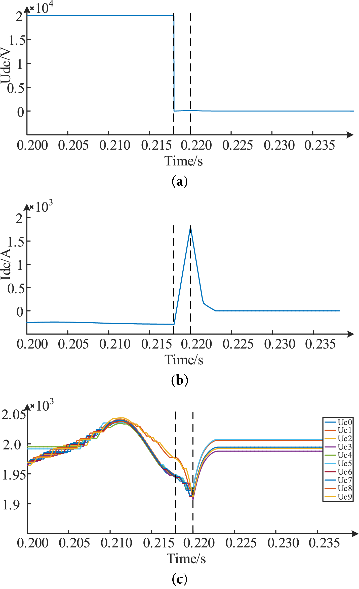
Figure 14: DC waveform of failure. (a) voltage waveform of DC side. (b) current waveform of DC side. (c) capacitor voltage waveform
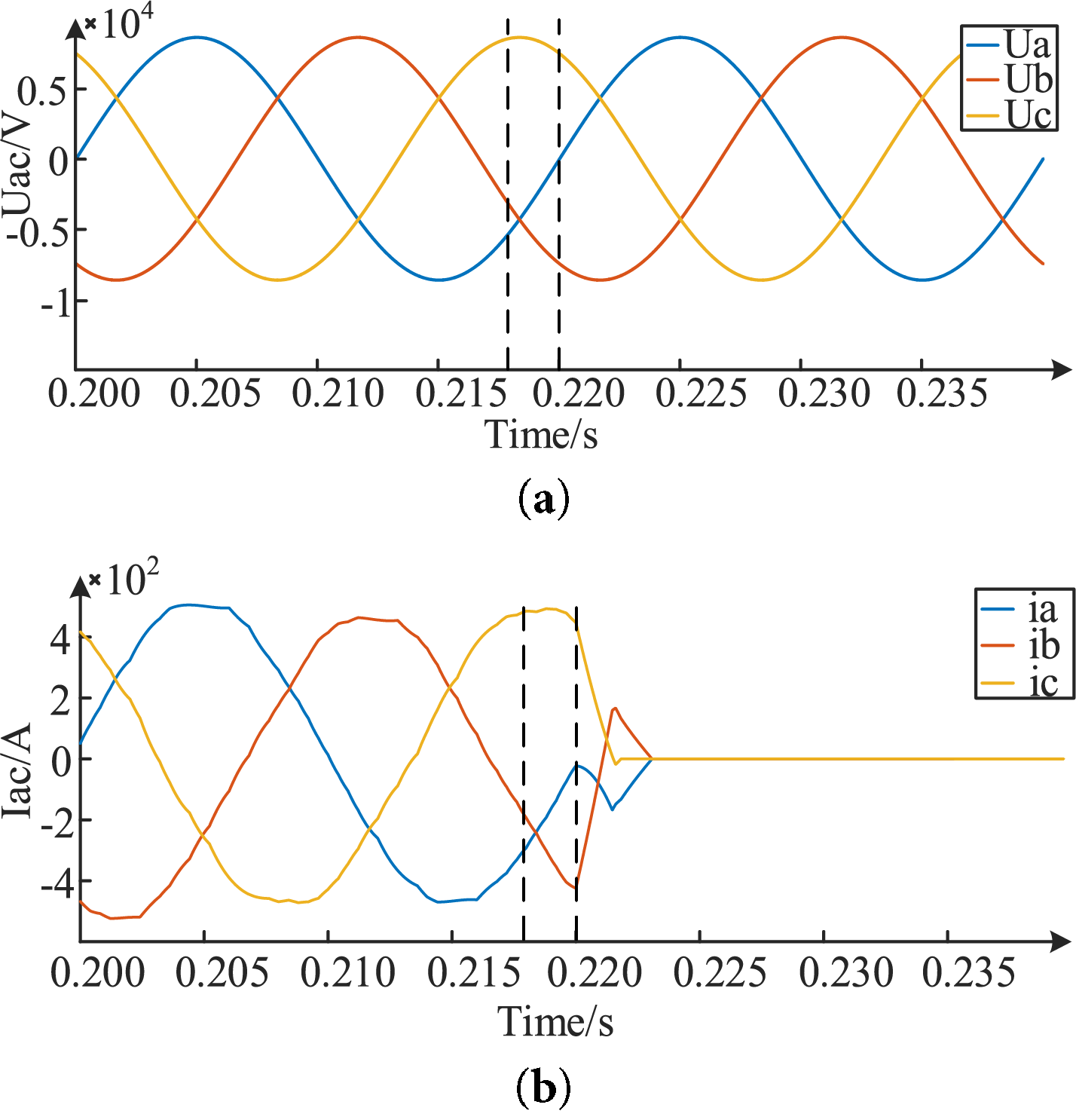
Figure 15: AC waveform of failure. (a) voltage waveform of AC side. (b) current waveform of AC side
The waveform analysis of Fig. 14a,b shows that the system was in a stable operating state before the fault occurred, with the DC bus voltage maintained at 20 kV and the current stabilized at −300 A. In Fig. 14a, when a bipolar short circuit occurred at 0.218 s, the DC voltage instantly dropped to zero. As shown in Fig. 14b, during the fault detection period (0.218–0.22 s), the DC current surged sharply from the initial value of −300 A to a peak of 1.8 kA. The fault current in this stage was mainly supplied by the discharge of energy storage capacitors. Observing Fig. 14c, it can be seen that the capacitor voltage continued to decrease in the early stage of the fault, indicating that the energy storage elements were releasing energy. As shown in the second half of Fig. 14b, after the system was blocked, the capacitor switched to the charging mode, and the established back electromotive force effectively suppressed the fault current. This process caused the current to rapidly decay from 1.8 kA to zero, successfully achieving fault clearance. The rise trend of the capacitor voltage intuitively reflects the formation process of the back electromotive force, verifying the effectiveness of the fault blocking mechanism.
Analysis of the waveform data in Fig. 15 shows that before the DC bipolar short-circuit fault occurred, the voltage and current characteristics of the AC port were completely consistent with those during steady-state operation. In the initial fault stage (0.218–0.22 s), since the IGBTs had not yet been blocked, the sub-modules continued to perform switching operations in the normal working mode, and the fault current persisted during this period. When the system implemented full blocking at 0.22 s, the AC current rapidly decayed to zero. Throughout the entire process from fault occurrence to complete clearance, the AC voltage waveform remained stable without obvious distortion, and its amplitude and phase characteristics were consistent with the voltage waveform under normal operating conditions.
In order to compare the fault blocking capability of the proposed topology and the traditional CDSM, the time of fault current clearing of the two topologies is shown in Fig. 16. After blocking, the arm current and the DC current of proposed topology are reduced to zero in about 2.5 ms, while the fault clearing time of the traditional CDSM is about 5 ms, which doubles the fault clearing speed and is more conducive to the safe and stable operation of the system.
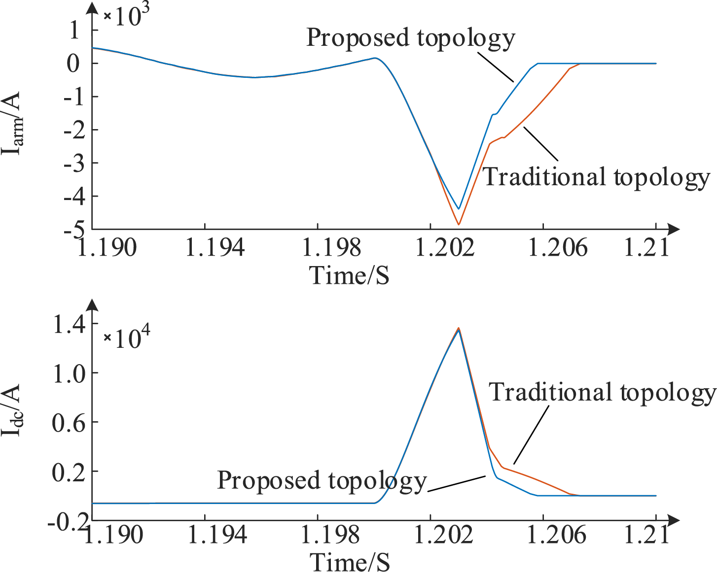
Figure 16: Comparison of fault clearing speed
For quantitative analysis the delay-tolerance discussion, the simulations with fault delay times ranging from 2 to 10 ms are conducted to verify the blocking effectiveness of the proposed topology. The results are presented in Figs. 17–19 and Table 5, showing that the peak current increases with longer blocking delay times. Considering that the peak current becomes excessively high when the blocking delay exceeds 6 ms, due to space limitations, only the peak fault current and fault clearing time for blocking delays from 6 to 10 ms are listed in the table. As shown in the figures and table, although the blocking delay time increases, the proposed topology can still effectively clear faults.
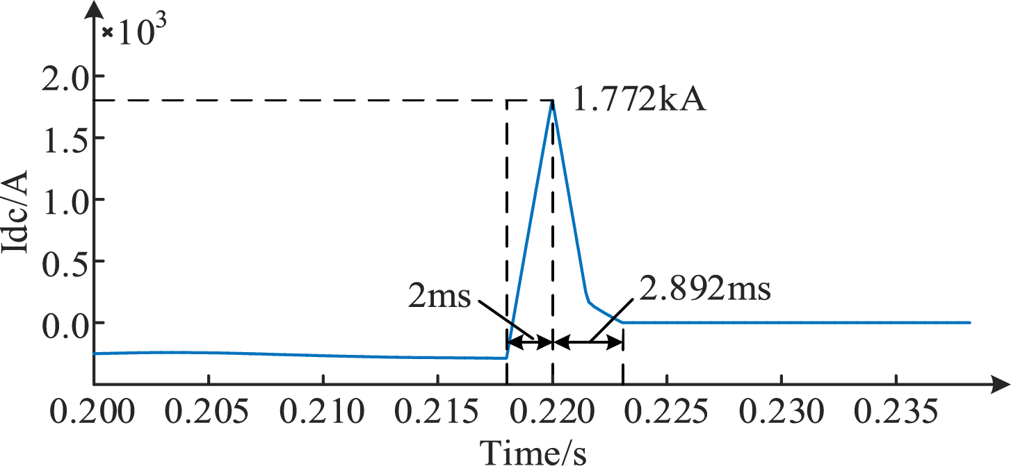
Figure 17: The current waveform of DC side when the delay time is 2 ms
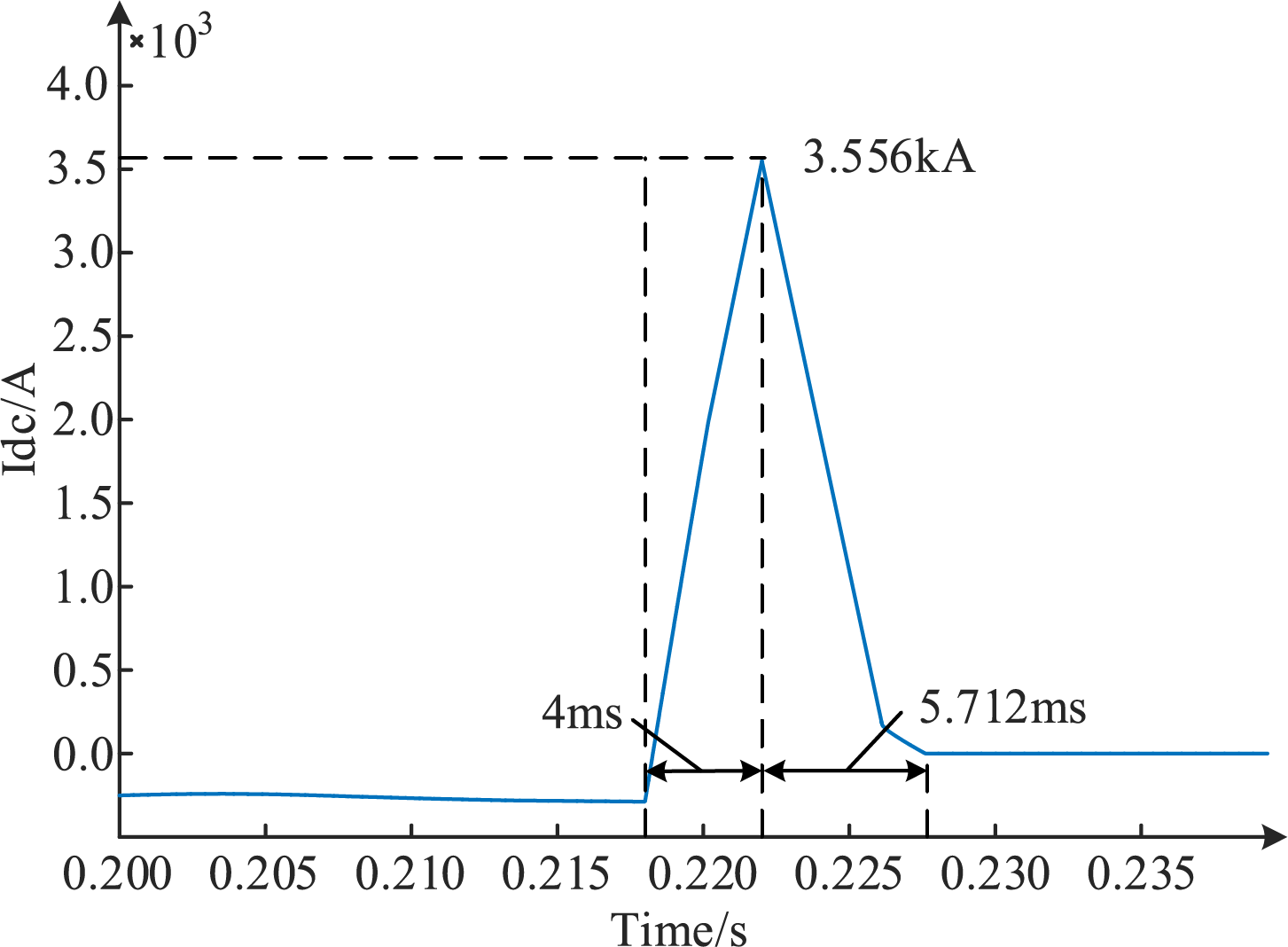
Figure 18: The current waveform of DC side when the delay time is 4 ms
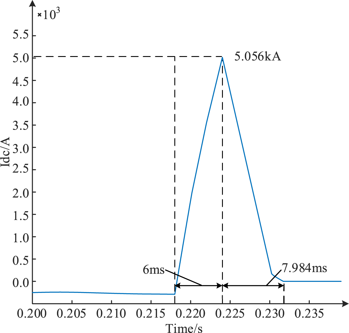
Figure 19: The current waveform of DC side when the delay time is 6 ms

To experimentally validate the performance of the proposed control scheme, a real-time simulation platform was established using RT-LAB. As illustrated in Fig. 20 and detailed in Table 6, the platform comprises an OPAL-RT OP5600 (Chongqing University, Chongqing, China), real-time simulator and a StarSim MT1070 unit for rapid control prototyping (RCP). In this configuration, the OP5600 emulates the plant model (i.e., the grid-connected photovoltaic-storage integration system), while the control algorithms are executed on the MT1070. The two units are interfaced via TCP/IP communication with a sampling period of 50 μs. To address the critical issue of communication delays and ensure closed-loop stability, the StarSim synchronization module was employed for real-time delay compensation.
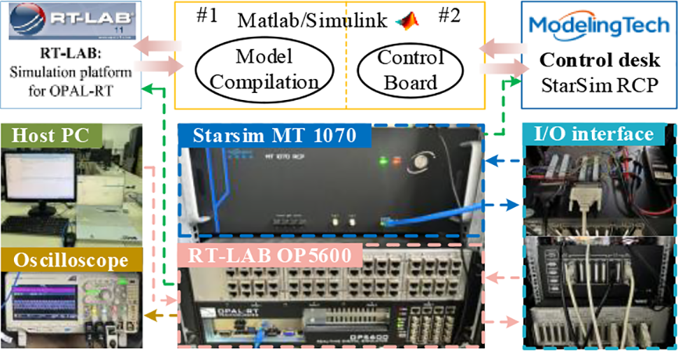
Figure 20: Real-time simulation verification platform
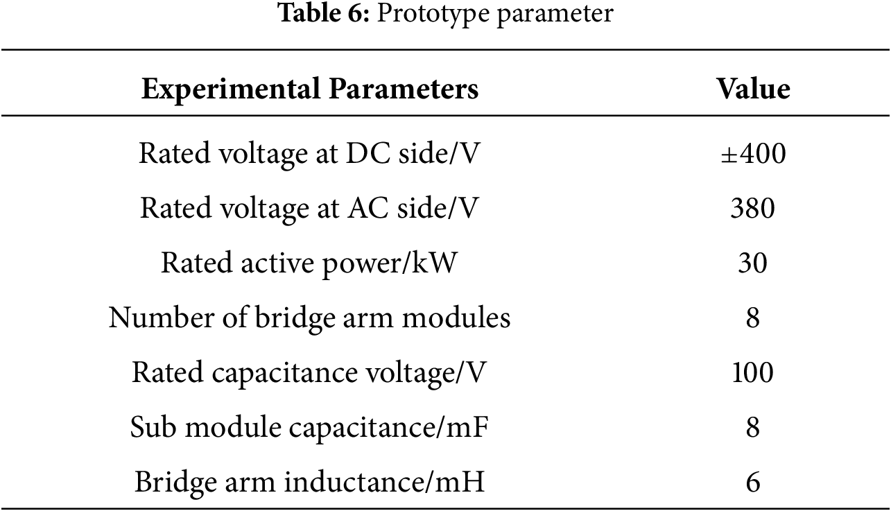
Fig. 21 shows the key electrical quantity waveforms during the stable operation of the system. With the new control scheme, the characteristics of the a-phase port are as follows: the peak value of the AC voltage reaches 307 V, the peak value of the current is 67 A, and the two are strictly synchronized. Observing the working state of the arm energy storage module, it can be seen that the voltage of each capacitor is maintained at around the design value of 100 V with small fluctuations, and the voltage deviation between different modules is controlled within a reasonable range.
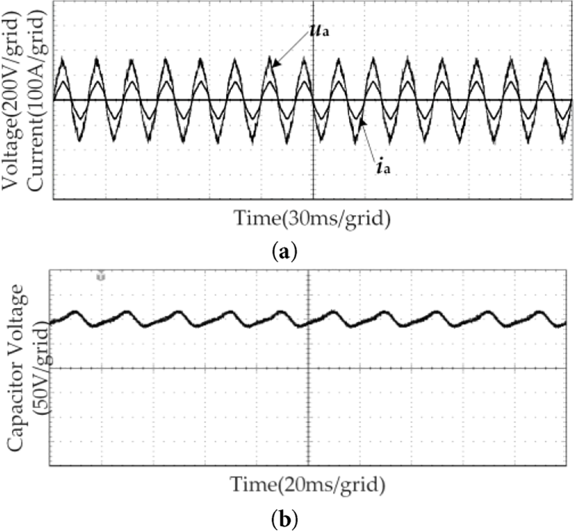
Figure 21: Steady-state operation waveform of integrated PV energy storage prototype. (a) AC side voltage and current waveform. (b) Capacitor voltage waveform
To evaluate the protection performance of the system under extreme fault conditions, a severe short-circuit condition was simulated by disconnecting the DC-side bipolar contactor. The dynamic response process of the AC port current measured in the experiment is shown in Fig. 22.
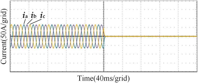
Figure 22: Fault cutting waveform of integrated PV energy storage prototype
In conclusion, under normal operating conditions, the CDESSM topology studied in this paper, combined with the developed control scheme, demonstrates good operational stability. Especially when a severe fault such as DC bipolar short circuit occurs, the topology can quickly block the fault current path through the back electromotive force established by the energy storage capacitor, achieving effective isolation of the DC-side fault.
To further enhance the engineering relevance of the proposed converter system, a long-duration real-time operation test was conducted using the RT-LAB platform. The objective of this test was to evaluate the endurance and long-term stability of the control algorithm and power-stage parameters under continuous operation. In the experiment, the PV–storage integrated converter was operated continuously for 60 s on the RT-LAB platform under rated conditions (30 kW, ±400 V DC bus). During the test, the AC-side current and controller computational load were continuously monitored, and the waveforms were recorded for the periods of 6–6.02 s and 54–54.02 s, as shown in Fig. 23. During the test, real-time data were recorded for the AC-side current, and controller computation load.
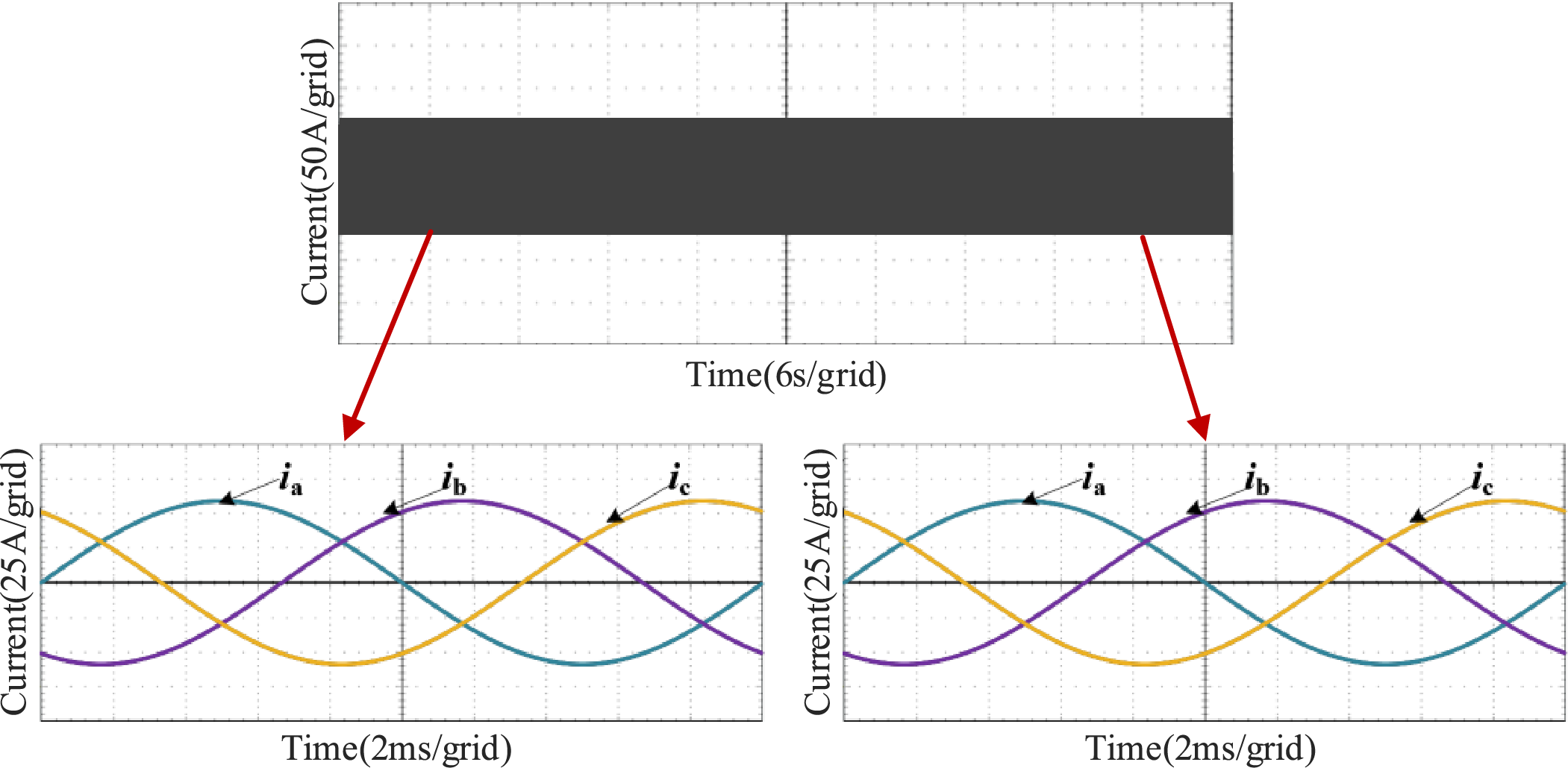
Figure 23: AC-side current
The recorded results demonstrate that all submodule capacitor voltages remained within ±5.2% of the nominal 100 V reference value throughout the entire period. The AC-side voltage and current maintained stable 50 Hz sinusoidal waveforms, with negligible harmonic distortion or phase drift. In addition, the processor utilization of the control algorithm remained steady at around 35%, and no cumulative delay or instability was observed.
These findings confirm that the proposed CDESSM topology and its dual-layer balancing control strategy are capable of maintaining reliable operation during long-term continuous operation, without noticeable degradation in voltage balancing or modulation performance.
Beyond the numerical simulations and prototype experiments, the proposed CDESSM-based photovoltaic-storage integration system demonstrates strong potential for practical deployment. Its inherent ability to independently clear DC faults and maintain balanced power device losses makes it particularly suitable for distributed PV plants, industrial energy storage parks, and off-grid microgrids that demand high reliability and rapid fault protection.
5.5 Scalability and Computational Load Analysis
To further evaluate the applicability of the proposed converter for MW-level photovoltaic-storage systems, a theoretical scalability assessment is performed. When system capacity increases from several tens of kilowatts to several megawatts, both the DC-link voltage and phase current scale approximately linearly with rated power. Since each Clamp Double Energy Storage Submodule (CDESSM) maintains a fixed capacitor voltage (typically 1–2 kV) and switching frequency, the total number of submodules N grows proportionally with the DC bus voltage UDC, which can be expressed as
For a 20 kV DC bus and submodule capacitor voltage UC = 2 kV, about five submodules per arm are required, and even at higher voltages the computational load increases only linearly with N.
The proposed control scheme mainly involves sorting capacitor voltages and allocating switching states in each sampling cycle. Its algorithmic complexity is approximately O(N log N). Considering the same 50 μs sampling period used in the prototype, the estimated execution time per cycle is less than 25 μs on a 200 MHz digital signal processor, corresponding to around 50% processor utilization. This indicates that real-time operation can be achieved without additional hardware acceleration, even when dozens of submodules are used.
Moreover, the DC fault-blocking mechanism of the CDESSM depends primarily on the local capacitor back-EMF and arm inductance. These parameters are determined by submodule design and do not vary with overall system scale. Therefore, when identical submodule parameters are maintained, the DC fault clearing time (approximately 2–3 ms as observed in Section 5.2) remains nearly unchanged for MW-level operation.
In summary, the above theoretical analysis confirms that both the computational complexity and fault-handling performance of the proposed CDESSM topology scale favorably with system capacity. Hence, the converter and control framework can be feasibly extended to MW-level photovoltaic–storage integration without excessive computational or hardware burden.
This study presents a photovoltaic–energy storage integrated converter based on the clamped dual-energy storage submodule (CDESSM) topology. A conduction-time-balanced nearest level modulation (NLM) algorithm and a dual-layer capacitor voltage balancing control strategy are developed to enhance voltage equalization and device utilization. Simulation and RT-LAB prototype results confirm that the proposed system operates stably under laboratory conditions, with submodule capacitor voltage deviation maintained within 5.5%. Under DC fault conditions, the converter achieves rapid fault current suppression and isolation within the millisecond range. Furthermore, long-term RT-LAB operation tests verify the system’s stability during continuous operation, with no observable controller drift. Overall, the proposed topology and control strategy demonstrate excellent dynamic performance, stability, and engineering feasibility within the tested scope.
Acknowledgement: This work was supported by Science and Technology Project of State Grid Sichuan Electric Power Company.
Funding Statement: This work was supported by the Science and Technology Project of State Grid Sichuan Electric Power Company, Grant No. SGSCJY00NYJS2400066.
Author Contributions: Conceptualization, Fan Shao; methodology, Xingqi He; validation, Fan Shao, Ao Li and Yalu Hu; writing—original draft preparation, Fan Shao and Yufan Chen; writing—review and editing, Fan Shao. All authors reviewed the results and approved the final version of the manuscript.
Availability of Data and Materials: Not applicable.
Ethics Approval: Not applicable.
Conflicts of Interest: The authors declare no conflicts of interest to report regarding the present study.
References
1. Dabra V, Paliwal KK, Sharma P, Kumar N. Optimization of photovoltaic power system: A comparative study. Prot Control Mod Power Syst. 2017;2(1):1–11. doi:10.1186/s41601-017-0036-2. [Google Scholar] [CrossRef]
2. Mahmood H, Michaelson D, Jin J. Decentralized power management of a PV/Battery hybrid unit in a droop-controlled islanded Microgrid. IEEE Trans Power Electron. 2015;30(12):7215–29. doi:10.1109/TPEL.2015.2394351. [Google Scholar] [CrossRef]
3. Chen J, Chen H, Liang Z. An exergy analysis model for the optimal operation of integrated heat-and-electricity-based energy systems. Prot Control Mod Power Syst. 2024;9:1–18. doi:10.23919/PCMP.2023.000270. [Google Scholar] [CrossRef]
4. Li X, Yao L, Hui D. Optimal control and management of a large-scale battery energy storage system to mitigate fluctuation and intermittence of renewable generations. J Mod Power Syst Clean Energy. 2016;4:593–603. doi:10.1007/s40565-016-0247-y. [Google Scholar] [CrossRef]
5. Chen W, Wang G. Decentralized voltage-sharing control strategy for fully modular input-series-output-series system with improved voltage regulation. IEEE Trans Ind Electron. 2015;62:2777–87. doi:10.1109/TIE.2014.2365433. [Google Scholar] [CrossRef]
6. Li X, Wang L, Yan N, Ma R. Cooperative dispatch of distributed energy storage in distribution network with PV generation systems. IEEE Trans Appl Supercond. 2021;31(8):1–4. doi:10.1109/TASC.2021.3117750. [Google Scholar] [CrossRef]
7. Sutikno T, Arsadiando W, Wangsupphaphol A, Yudhana A, Facta M. A review of recent advances on hybrid energy storage system for solar photovoltaics power generation. IEEE Access. 2022;10:42346–64. doi:10.1109/ACCESS.2022.3165798. [Google Scholar] [CrossRef]
8. Zhang X, Jin J. MMC-based PV grid-connected system with SMES-battery hybrid energy storage. In: Proceedings of the 2023 IEEE International Conference on Applied Superconductivity and Electromagnetic Devices (ASEMD); 2023 Oct 27–29; Tianjin, China. p. 1–2. [Google Scholar]
9. Yan S, Shen Q, Li X, Li S, Chu E. SOC balancing control based on multi-agent for multiple energy storage units in MMC high power energy storage system. CSEE J Power Energy Syst. 2025;11(3):1253–61. doi:10.17775/CSEEJPES.2021.08350. [Google Scholar] [CrossRef]
10. Zhang X, Feng G. MMC-based PV grid-connected system with SMES-battery hybrid energy storage system. IEEE Trans Appl Supercond. 2024;34(8):1–4. doi:10.1109/TASC.2024.3420187. [Google Scholar] [CrossRef]
11. Wang R, Li Z, Wen X, Liu N, Wang X. A novel MMC sub-module topology with DC fault clearance capability. IEEE Access. 2019;7:96085–93. doi:10.1109/ACCESS.2019.2923268. [Google Scholar] [CrossRef]
12. Shen Z, Dinavahi V. Real-time MPSoC-based electrothermal transient simulation of fault tolerant MMC topology. IEEE Trans Power Deliv. 2019;34(1):260–70. doi:10.1109/TPWRD.2018.2866562. [Google Scholar] [CrossRef]
13. Wang B, Tian J, Zhang X, Yang R, Mu W, Zhou X. Integration of a clamp double submodule based on integrated chips for MMC reliability improvement. IEEE J Emerg Sel Top Power Electron. 2024;12(6):5817–27. doi:10.1109/JESTPE.2024.3380904. [Google Scholar] [CrossRef]
14. Song Y, Luo Y, Xiong X. Loss distribution analysis and accurate calculation method for bulk-power MMC. Prot Control Mod Power Syst. 2023;8(1):1–15. doi:10.1186/s41601-023-00313-x. [Google Scholar] [CrossRef]
15. Siemaszko D. Fast sorting method for balancing capacitor voltages in modular multilevel converters. IEEE Trans Power Electron. 2015;30(1):463–70. doi:10.1109/TPEL.2014.2312101. [Google Scholar] [CrossRef]
16. Jin Y, Wang S, Xiao Q. A novel harmonic control method for MMC combining improved nearest level control and selective harmonic elimination method. In: Proceedings of the 2019 IEEE Energy Conversion Congress and Exposition (ECCE); 2019 Sep 29–Oct 3; Baltimore, MD, USA. [Google Scholar]
17. Huang M, Zou J, Ma X. Hybrid modular multilevel converter with redistributed power to reduce submodule capacitor voltage fluctuation. IEEE Trans Power Electron. 2018;33:6595–607. doi:10.1109/TPEL.2017.2755763. [Google Scholar] [CrossRef]
18. Zeng R, Xu L, Yao L, Williams BW. Design and operation of a hybrid modular multilevel converter. IEEE Trans Power Electron. 2015;30:1137–46. doi:10.1109/TPEL.2014.2320822. [Google Scholar] [CrossRef]
19. Lin Y, Lin L, Xu C, Hu J. A design method of hybrid modular multilevel converter with negative output generated by FBSM. In: Proceedings of the IECON 2017-43rd Annual Conference of the IEEE Industrial Electronics Society; 2017 Oct 29–Nov 1; Beijing, China. p. 4465–71. [Google Scholar]
20. Jiang Q, Tao Y, Li B. Joint limiting control strategy based on virtual impedance shaping for suppressing DC fault current and arm current in MMC-HVDC systems. J Mod Power Syst Clean Energy. 2023;11:2003–14. doi:10.35833/MPCE.2022.000571. [Google Scholar] [CrossRef]
21. Lai J, Chen J, Yin X, Liang J, Jiang L, Zeng X, et al. Principle and implementation of active ground fault arc suppression based on hybrid MMC in AC/DC distribution network. IEEE Trans Power Deliv. 2024;40:2503–19. doi:10.1109/TPWRD.2025.3577921. [Google Scholar] [CrossRef]
22. Uwagboe JO, Saha AK. A comprehensive review of multilevel inverter topologies and control strategies for grid-connected photovoltaic battery energy storage systems integrating active power filter. IEEE Access. 2025;13:169989–70016. doi:10.1109/ACCESS.2025.3615104. [Google Scholar] [CrossRef]
23. Hong Y, Apolinario GFD, Lee Y, Jiang J, Yeh J. Short-circuit analysis of inverter-based distributed generation and energy storage system with different control modes. IEEE Trans Power Electron. 2025;40:17218–33. doi:10.1109/TPEL.2025.3588845. [Google Scholar] [CrossRef]
24. Zhang Z, Xu Z, Xue Y. Valve losses evaluation based on piecewise analytical method for MMC-HVDC links. IEEE Trans Power Deliv. 2014;29(3):1354–62. doi:10.1109/TPWRD.2014.2304724. [Google Scholar] [CrossRef]
Cite This Article
 Copyright © 2026 The Author(s). Published by Tech Science Press.
This work is licensed under a Creative Commons Attribution 4.0 International License , which permits unrestricted use, distribution, and reproduction in any medium, provided the original work is properly cited.
 Downloads
 Citation Tools
