
 Submit a Paper
 Propose a Special lssue
 Open Access
ARTICLE

DFT-Based Study of Structural, Electronic, Optical and Elastic Properties of CdGeAs2 and CdSnAs2 Chalcopyrires
1 UDERZA Unit, Faculty of Technology, University of El Oued, El Oued, Algeria
2 Institute of Sciences, University Center of Tipaza, Tipaza, Algeria
3 LPR Laboratory, Department of Physics, Faculty of Science, Badji Mokhtar University, Annaba, Algeria
4 L3M Metallurgy Materials and Mining Laboratory, National Higher School of Technology and Engineering, Annaba, Algeria
5 Algeria Civil Engineering Department, Institute University of Tipaza, Tipaza, Algeria
6 École Normale Supérieure de Ouargla, Ouargla, Algeria
* Corresponding Authors: Y. Megdoud. Email: ; Y. Benkrima. Email:
Chalcogenide Letters 2026, 23(2), 5 https://doi.org/10.32604/cl.2026.076585
Received 13 September 2025; Accepted 23 November 2025; Issue published 28 February 2026
 View Full Text
 Download PDF
Abstract
This study reports a comprehensive first-principles investigation of the chalcopyrite semiconductors CdGeAs2 and CdSnAs2, with particular emphasis on their structural, electronic, optical, and elastic properties. The calculations were carried out within the density functional theory (DFT) framework using the full-potential linearized augmented plane wave (FP-LAPW) method. The optimized equilibrium structural parameters, including lattice constants a and c as well as the internal coordinate u, show very good consistency with available experimental measurements and earlier theoretical predictions. Band structure calculations confirm that both compounds exhibit direct band gaps, which makes them attractive candidates for photovoltaic and optoelectronic devices. Additionally, the optical response exhibits strong absorption within the visible region, while the calculated elastic constants confirm the mechanical stability of these materials.Keywords
Rising global energy needs coupled with environmental challenges have intensified the search for sustainable energy technologies. Among the various alternatives, solar energy conversion is recognized as one of the most effective substitutes for fossil fuels. Solar radiation is practically unlimited on the human timescale, positioning it as a clean and renewable source that minimizes ecological impact. Achieving efficient solar utilization requires the design of advanced semiconductors with well-suited optoelectronic characteristics. In this context, compounds belonging to the I–III–VI2 and II–VI–V2 families [1,2,3] have attracted particular attention for photovoltaic devices, owing to their appropriate bandgap ranges and high absorption capabilities in the visible spectrum (on the order of 105 cm−1). Among these materials, CdXAs2 (X = Ge and Sn) compounds belong to the I-III-VI2 class, which can be derived from binary II-VI semiconductors such as ZnS, which crystallize in a zinc blende structure. The ordered substitution of Zn cations by Cu (group I) and X (group III: Al, Ga, In) leads to structural modifications, transforming the symmetry from cubic to tetragonal, with a space group I̅42d [4,5]. This structural change also affects the lattice parameter ratio (c/a), which typically approaches or slightly deviates from 2 in most cases. The anisotropic nature of these compounds results in birefringence, which plays a crucial role in their optical behavior. This birefringence enables phase-matching conditions by angular tuning, making these materials highly relevant for laser applications, such as CO2 lasers. In high-altitude regions, where solar radiation remains intense and nearly four times stronger than at the Earth’s surface, high-power lasers based on CdXAs2 compounds [6,7,8] could be deployed in geostationary orbits to capture and redirect solar energy toward terrestrial photovoltaic systems. This strategy reduces lateral dispersion and improves the efficiency of energy transfer. A number of theoretical studies have previously investigated the electronic and optoelectronic behavior of CdXAs2 compounds. For example, Zhang Xian-Zhou reported their band structures using the Perdew–Burke–Ernzerhof (PBE-GGA) functional, while Anima Ghosh applied the Tran–Blaha modified Becke–Johnson (mBJ-GGA) scheme to obtain more accurate bandgap estimations. Further analyses by Wenfeng Li and Xue Li addressed both electronic and thermoelectric characteristics of these materials within the mBJ-GGA framework. On the experimental side, Bodnar provided measurements of the thermal behavior of the CdXAs2 family.
Despite earlier contributions, several important features of CdXAs2 compounds have not yet been thoroughly investigated. In particular, systematic analyses of the optoelectronic response of CdGeAs2 and CdSnAs2, with emphasis on their birefringence, are still limited. The present study seeks to fill this gap by offering the first theoretical prediction of birefringence in these systems. In contrast to previous works that concentrated mainly on electronic aspects, we highlight how the substitution of the X-cation (Ge versus Sn) influences the structural, electronic, and optical behavior of the crystals [9,10,11]. Such knowledge is vital for tailoring these semiconductors for photovoltaic and broader optoelectronic applications. Furthermore, little attention has been devoted to thermal characteristics in past computational efforts [12,13,14,15]. Except for the contribution of Sheetal Sharma et al. [16,17,18], where CdGeAs2 and CdSnAs2 were examined, first-principles investigations into their thermal performance remain rare. Evaluating thermal properties is fundamental to understanding their stability under different pressure and temperature regimes [19], especially in cases lacking experimental confirmation [20]. These insights also help refine crystal growth procedures and ensure the fabrication of high-quality samples for technological use. Objective of the Study: The central objective of this work is to close the identified research gaps by carrying out an extensive first-principles study of CdXAs2 semiconductors (X = Ge, Sn). Within the framework of density functional theory (DFT) and using the FP-LAPW approach, we investigate their structural, electronic, optical, and thermal characteristics. Particular attention is given to the influence of X-site substitution on lattice parameters, band structures, and optical responses such as birefringence and phase-matching, in order to evaluate their potential for photovoltaic and laser applications. In addition, thermal behavior under different pressure and temperature conditions is analyzed to determine performance in demanding environments. Theoretical outcomes are compared with reported experimental data to verify accuracy and reliability. Through this integrated approach, the study provides meaningful guidance for experimental advancements and the deployment of CdXAs2 compounds in cutting-edge optoelectronic and energy-conversion devices.
In this work, the WIEN2k_2021 computational package [21] was employed to study the structural, electronic, elastic, and optical properties of CdGeAs2 and CdSnAs2. This code is grounded in the full-potential linearized augmented plane wave (FP-LAPW) formalism implemented within the framework of density functional theory (DFT) [22]. The FP-LAPW method is widely acknowledged for its high precision in describing low-symmetry crystal structures and materials containing heavy elements, as it treats both the potential and charge density without shape approximations. To describe the exchange–correlation effects (Vxc), which account for many-body electron interactions, different approximations were adopted depending on the targeted physical properties. Structural optimizations were carried out using the Wu–Cohen generalized gradient approximation (WC-GGA), known for its reliable description of equilibrium geometries through the inclusion of both local electron density and its gradient. In contrast, electronic band gap calculations were performed using the modified Becke–Johnson (mBJ) potential [23], a semi-empirical approach that significantly improves band gap predictions for insulators and semiconductors. Inside the FP-LAPW framework, the two distinct regions resulting from the division of the unit cell. Inside the muffin-tin spheres surrounding each atomic site, the wave functions are expanded in spherical harmonics up to a maximum angular momentum of ℓmax = 10. In the interstitial region between these spheres, both the wave functions and the potential are described using plane-wave expansions. the parameter RMT·Kmax is the controller of the plane-wave basis set, which was fixed at a value of 8 for all calculations, wherever RMT denotes the minutest muffin-tin ambit and Kmax represents the maximum mutual lattice vector. Additionally, the Fourier expansion cutoff for the charge density was set to Gmax = 12 Ry, ensuring an accurate representation of the total electrostatic potential [24]. Overall, the chosen computational settings and methodological approach were carefully optimized to guarantee robust and reliable predictions of the physical properties of the studied chalcopyrite materials.
3.1 Structural Characterization
In Fig. 1, structural analysis forms the basis of our research. If the structure is not correctly determined, subsequent predictions regarding the mechanical and optoelectronic properties of the material will not be reliable. The crystal geometry plays a decisive role in governing atomic arrangements and electronic interactions within the material. Consequently, achieving an optimized structural configuration is a prerequisite before undertaking more advanced computational analyses. In this context, the present study aims to accurately determine key crystallographic parameters, including the lattice amounts a0 and c0, the tetragonal distortion ratio (c/a), the equilibrium volume V0, the interior positional constraint u, the isothermal bulk modulus B0, and its first pressure derivative B′0 [25].
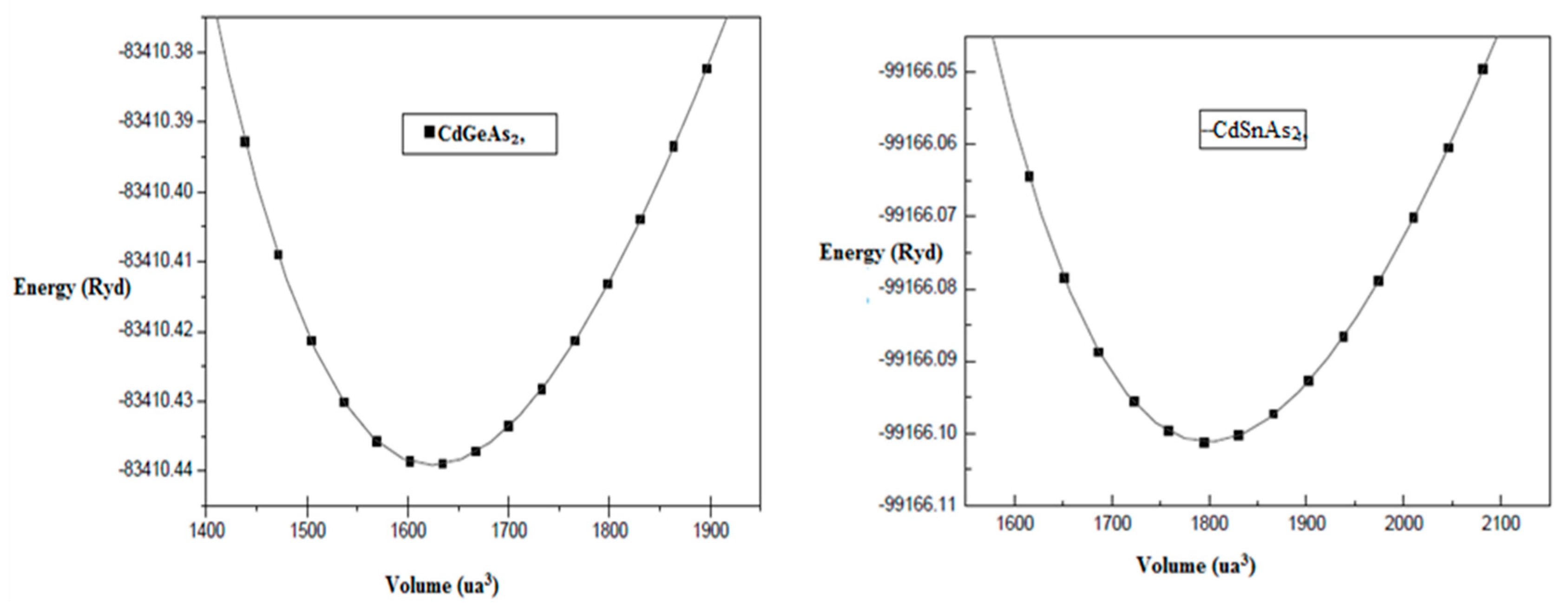
Figure 1: Total energy as a function of unit-cell volume for CdGeAs2 and CdSnAs2 compounds.
We calculate the energy volume data Etot is fitted to the Murnaghan equation of state:
- This formalism enables the determination of several fundamental physical parameters, namely: E0, corresponding to the minimum full energy at the pounded state; V0, representing the equilibrium volume;
- B0, which quantifies the material’s resistance to volumetric compression; and B′0, denoting the first pressure derivative of the bulk modulus and reflecting the nonlinear elastic response under applied pressure.
The lattice parameters a0, c0, equilibrium volume V0 the bulk modulus B0, and its pressure derivative
From Table 1, we observe that:
The calculated lattice parameters for CdGeAs2 and CdSnAs2 show excellent agreement with both experimental values and previous theoretical studies, with deviations generally below 1%. This level of agreement demonstrates the reliability of the FP-LAPW method used within the DFT formalism, particularly with the WC-GGA approximation known to improve structural predictions compared to standard GGA or LSDA functionals. The calculated lattice constants follow the expected chemical trend: CdSnAs2 has larger lattice constants than CdGeAs2, which is unswerving with the higher atomic radius of in related to Ge, this reflects a natural expansion of the unit cell when Ge is replaced by In, leading to an increased interatomic spacing.
The bulk modulus B0 is a measure of the material’s resistance to volume compression and provides insight into its mechanical stiffness. The value obtained for CdGeAs2 is in good agreement with previously reported theoretical studies [13,15], confirming the reliability of the present computational approach. In contrast, no experimental bulk modulus data are available for CdSnAs2. However, the predicted lower B0 value follows the expected chemical trend, since the larger atomic size and weaker bonding of Sn compared to Ge result in reduced mechanical rigidity.
This is physically meaningful and supports the idea that CdGeAs2 is mechanically more robust, making it potentially more suitable for applications where mechanical stability under pressure is important (e.g., thin-film photovoltaic devices). The pressure derivative
The detailed structural analysis confirms the thermodynamic and mechanical stability of both CdGeAs2 and CdSnAs2 in their chalcopyrite forms. The observed trends in lattice parameters and bulk moduli align with chemical intuition and available experimental data, validating the accuracy of the FP-LAPW method and the choice of the WC-GGA functional for these materials [27].
These results serve as a solid foundation for the subsequent electronic, optical, and thermoelectric analyses, and support the use of these compounds especially CdGeAs2 in applications re-quiring both stability and tunable properties, such as in photovoltaics, optoelectronics, and thermo-electric [28].
3.2 Analysis of the Structure Band of Electronic
The importance of theoretical research on solids based on electronic band structures, as it reveals their conductive behavior, semiconducting or metallic nature, and optical response. In this work, we analyzed the band structures of CdGeAs2 and CdSnAs2 chalcopyrite compounds, focusing on the band gap type and magnitude as well as the dispersion of electronic states [29].
The relative positioning of the VBM and CBM provides a definitive way to identify a material’s gap type. If both the highest energy of the valence band and the lowest energy of the conduction band occur at the same momentum point, the material is direct-gap. This specific electronic arrangement is ideal for high-performance photovoltaics because it significantly enhances how the material interacts with light.
A material’s interaction with radiation is fundamentally determined by its band gap (the energy offset between the VBM and CBM). For photovoltaic purposes, the optimal window is approximately 0.8 to 1.8 eV. Materials falling below this range may boost carrier concentration but risk higher leakage currents, whereas those with larger gaps are specifically advantageous for high-voltage systems and UV sensors, even if they absorb less of the visible spectrum.
Furthermore, the shape of the bands provides evidence on carrier agility: flat bands imply localized electrons with limited mobility, while dispersive bands indicate delocalized states and improved transport characteristics, this analysis is therefore crucial in evaluating the suitability of CdGeAs2 and CdSnAs2 for energy conversion applications.
Fig. 2 shows the structure of the calculated electronic energy bands for the chalcopyrite compounds CdGeAs2 and CdSnAs2 along the principal symmetry directions of the Brillouin zone, calculated using the modified Beck-Johnson potential (mBJ). These diagrams are fundamental to understanding the electronic behavior of the compounds and allow for the determination of the type and value of the band gap (Eg).
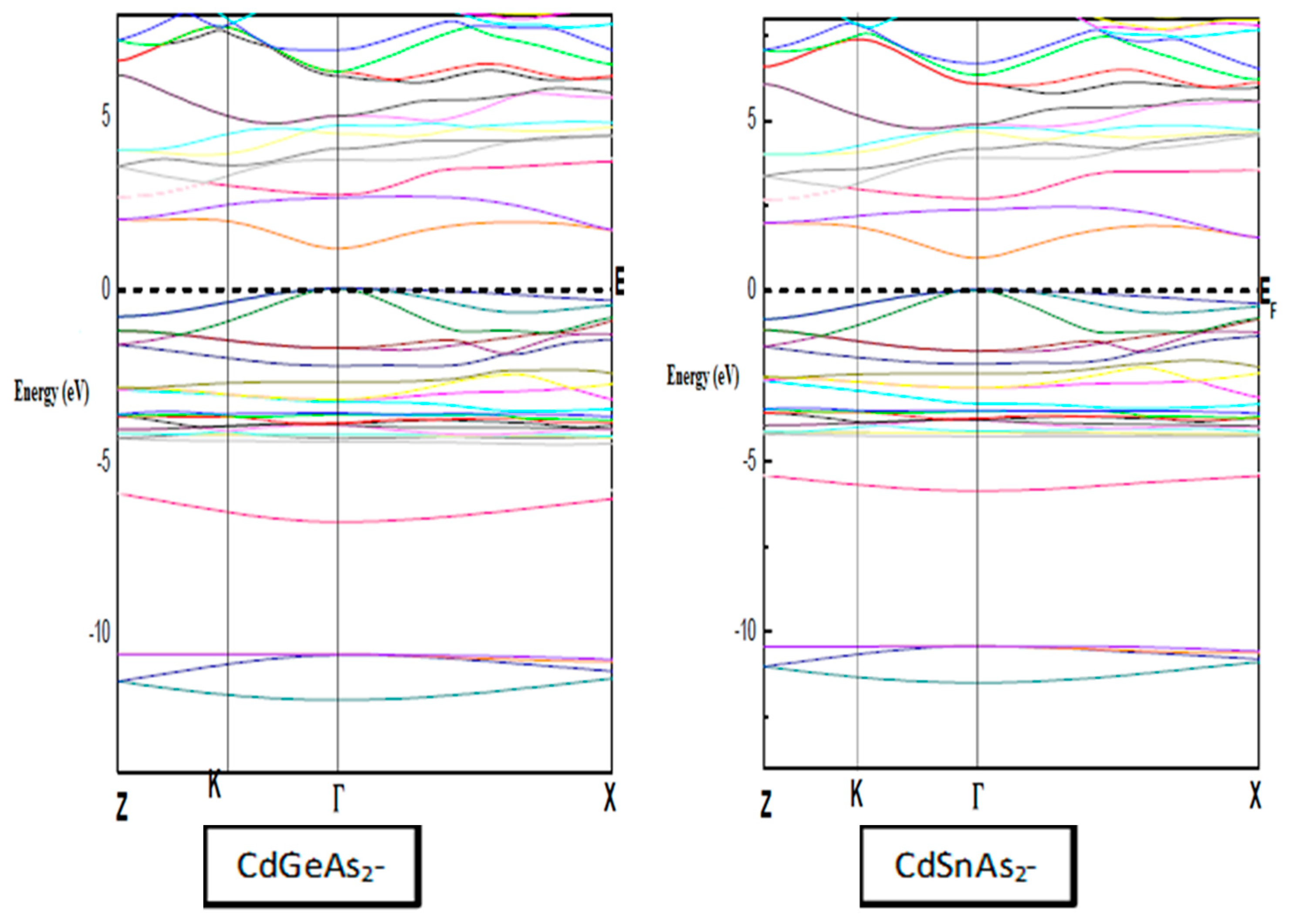
Figure 2: Structure Band of CdGeAs2 and CdSnAs2 compounds using the mBJ approximation.
Our results indicate that the overall band structure profile remains almost unchanged when different exchange–correlation approximations (WC-GGA or mBJ) are applied, with the main variation being the relative positions of the bands, which influence the gap size.
For both compounds, the valence band maximum (VBM) and conduction band minimum (CBM) are located at the Γ point, confirming a direct Γ–Γ band gap. This property is particularly advantageous for optoelectronic uses since direct-gap semiconductors exhibit efficient absorption and emission of light.
The numerical values of the band gaps calculated with different functionals are compiled in Table 2, alongside available theoretical and experimental values from the literature [30,31,32,33].
The WC-GGA (Wu–Cohen GGA), This functional is well-suited for structural optimization but underestimates the band gap, which is a well-known limitation of standard Density Functional Theory (DFT). This is because DFT is optimized for ground-state properties, not exciting states like band gaps.
The modified Becke–Johnson (mBJ) potential was developed to reproduce the accuracy of more advanced electronic structure approaches, such as hybrid functionals or GW schemes, while significantly reducing the associated computational effort. In the present investigation, the application of the mBJ potential results in band gap values that closely match available experimental data, thereby confirming its reliability and suitability for electronic structure calculations of semiconductor materials.
Traditional DFT functionals (LDA/GGA) fail to reproduce the discontinuity in the exchange-correlation potential that occurs when an electron is added or removed this is crucial for describing excited-state properties. Their simple mathematical form lacks the flexibility to account for self-energy corrections, which results in significant band gap underestimations.
Although methods like GW (Green’s function and screened Coulomb interaction) provide higher accuracy, they are computationally expensive. The mBJ approach offers a valuable compromise: it improves the description of the exchange potential, leading to more realistic band gaps while remaining computationally efficient.
For impact of Atomic Number on Band Gap Values according to Table 2, we observe the following trend:
Eg(CdSnAs2) > Eg(CdGeAs2)This behavior can be understood in terms of valence electron delocalization:
- Gallium (Ge) valence electrons occupy the n = 4 shell (4s2 4p1).
- Etain (Sn) valence electrons occupy the n = 5 shell (5s2 5p1).
As the principal quantum number (n) increases, the valence electrons become more delocalized, i.e., they are less tightly bound to the nucleus and spread out more in space. This reduces the overlap between orbitals, thereby increasing the band gap. Conversely, electrons in lower shells (like Ge) are more localized, leading to smaller gaps due to stronger orbital interactions.
Thus, the difference in band gap values between CdGeAs2 and CdSnAs2 reflects fundamental atomic-scale effects on electronic structure.
This research demonstrates that CdGeAs2 and CdSnAs2 are direct energy band gap semiconductors, making them excellent candidates for optoelectronic technologies such as solar cells, LEDs, and photodetectors. From a computational perspective, the choice of exchange and correlation functions is crucial for accurately estimating the energy band gap; our results indicate that the mBJ potential provides the most accurate values. The observed variation in energy band gaps between germanium- and tin-based compounds is attributed to electron delocalization effects resulting from their atomic arrangement. Overall, the FP-LAPW method, when combined with the mBJ potential, provides a robust and reliable framework for exploring the electronic behavior of complex semiconductors.
This work not only confirms existing experimental trends but similarly demonstrates the predictive power of innovative DFT methods in materials design and engineering.
The interaction between electromagnetic waves and semiconductors determines their potential in electronic applications. A comprehensive understanding of these optical properties is essential for improving functional layers in solar cells, lasers, and other radiation-based devices, as outlined in the theoretical framework of this study.
Illumination of a semiconductor often triggers different optical responses, such as absorption, reflection, refraction, transmission, scattering, or emission. These phenomena are governed by how incoming photons couple with a material with the structure of electronic.
A suitable way to characterize these optical processes is through the complex dielectric function ε(ω), which defines the material’s response to incident electromagnetic radiation. From ε(ω), one can derive fundamental optical quantities, including the refractive index, absorption behavior, and reflectivity.
3.3.1 Complex Dielectric Function
The frequency-dependent dielectric function is defined as [12]: ε(ω) = ε1(ω) + iε2(ω)(3) ε1(ω) is the real part, representing the reactive (non-dissipative) the electric field is the basis of the polarization-induced response of the medium; ε2(ω) is the imaginary compound, associated with the absorption of photons via the transitions of electronic on interband.
The imaginary part ε2(ω), It is calculated from the principles of quantum mechanics and depends directly on the band structure. It can be expressed as:
Here
3.3.2 Complex Refractive Index
ñ(ω) = n(ω) + iK(ω)(6)The multifaceted refractive index relates directly to the dielectric role via:
ñ2(ω) = ε(ω)(7)The real part, n(ω), which describes the phase velocity of light in the intermediate, is given by:
To obtain an accurate value of the refractive index n(ω), it is important to consider both the real and imaginary components of the dielectric function ε(ω). In cases where experimental optical measurements are unavailable, researchers often rely on empirical or semi-empirical models to estimate n(ω) from the band gap Eg. Among these, several models are widely applied Ravindra et al. model:
Herve and Vandamme formula:
The refractive index was evaluated using the Reddy–Nazeer electronegativity-based relation:
These relations yield approximate refractive index values based on the electronic structure and bonding nature of the material.
3.3.3 Absorption Coefficient α(ω)
The absorption coefficient α(ω) quantifies how much light is absorbed by the material as it propagates through it. It is linked to the extinction coefficient k(ω) and wavelength λ via:
α(ω) = 4π/λ k(ω)(11)Alternatively, α(ω) can also be expressed using the dielectric function:
This relation illustrates that absorption depends on both the imaginary part of the dielectric function and the refractive index. The spectral dependence of α(ω) helps identify the photon energies at which strong absorption occurs typically near and above the energy band gap providing key insight into the optoelectronic suitability of the material.
The optical properties of the chalcopyrite compounds AgGaTe2 and CdSnAs2 were investigated using ab initio calculations based on the WC-GGA approximation (Generalized Gradient Approximation as proposed by Wu and Cohen). The lattice parameters employed in these simulations were those previously optimized during the structural property calculations to ensure an accurate description of the ground-state geometry.
To achieve high precision in evaluating interband optical transitions, a dense k-point mesh of 1500 points was utilized within the first Brillouin zone. This fine sampling of the reciprocal space ensures a reliable integration over the electronic states involved in optical phenomena such as absorption and refraction.
The optical constants were computed over a broad energy range is 0 to 40 eV, covering not only the visible region but also extending into the ultraviolet. This wide spectral window is essential for capturing high-energy transitions and understanding the full electronic response of the material.
Fig. 3 displays the variation of the real ε1(ω) and imaginary ε2(ω) parts of the dielectric function as a function of photon energy for AgGaTe2 and CdSnAs2 compounds. A strong spectral similarity is observed between the two materials, attributed to their common chalcopyrite-type crystal structure. However, slight differences in the position and intensity of the peaks highlight the subtle impact of the cationic species (Ga vs. Sn) on the electronic structure.
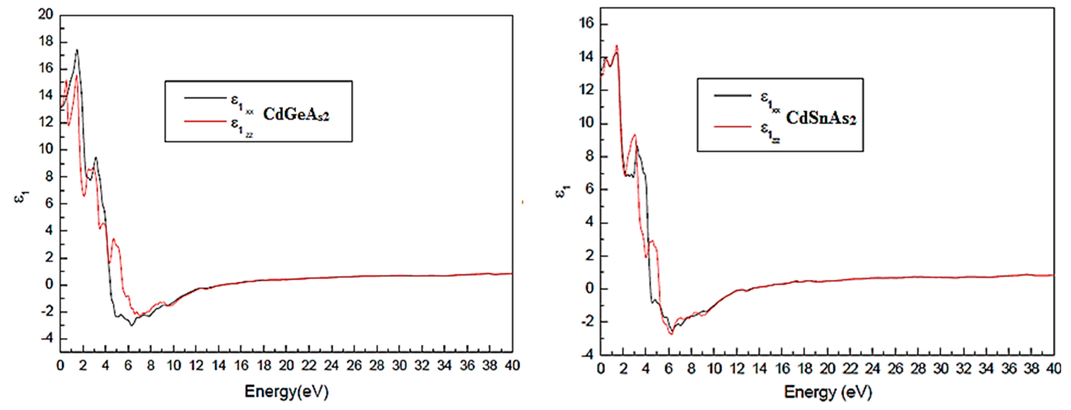
Figure 3: disparity of the real part of the insulator function ε1(ω) for CdGeAs2 and CdSnAs2 chalcopyrite compounds.
Due to the tetragonal symmetry of chalcopyrite structures, the optical response is characterized by two principal components: one perpendicular (ε⊥) and one parallel (ε||) to the crystallographic c-axis. Examination of the spectra reveals that the optical anisotropy is relatively weak in both compounds, especially for photon energies above 10 eV, where both components nearly overlap. This indicates quasihistorical optical behavior at high energies, which is particularly advantageous for non-polarized optical devices. Even at lower energies, the difference between ε⊥ and ε|| remains modest, reflecting a homogeneous electronic symmetry.
3.3.4 Dispersive Behavior ε1(ω) and Transparency
We observe that ε1(ω), the real dielectric component, becomes negative at certain frequencies, which points to strong internal reflective behavior. As illustrated in Fig. 3, the x- and y-directions show more pronounced negative features, indicating that energy losses are primarily transverse. This stands in contrast to AgInTe2, where the band structure’s anisotropic electron distribution causes the most substantial losses to occur along the z-direction.
The main peaks in ε1(ω) appear at 13.121 eV CdGeAs2 and 13.512 CdSnAs2. These peaks identify the dominant optical resonances, corresponding to interband transitions with strong coupling to the optical oscillator. ε1(ω) reaches zero in certain energy intervals (4.42–5.51 eV for CdGeAs2; 4.42–5.18 eV for CdSnAs2), indicating transparent behavior and low dispersion, due to the absence of optically allowed transitions in these regions-useful for designing optical windows.
3.3.5 Optical Absorption (ε2(ω)) and Absorption Onset
The imaginary part ε2(ω) provides critical insight into the optical interest properties of the material, as it is directly related to the density of accessible states for interbond conversions. The absorption thresholds occur at 1.17 eV for CdSnAs2 and 1.15 eV for CdGeAs2, in excellent agreement with theoretical predictions (~1.18 eV) and the direct band gap values obtained previously as shown in Fig. 4. These thresholds correspond to fundamental absorption edges, initiating shifts from the valence band extreme to the conduction band minimum.
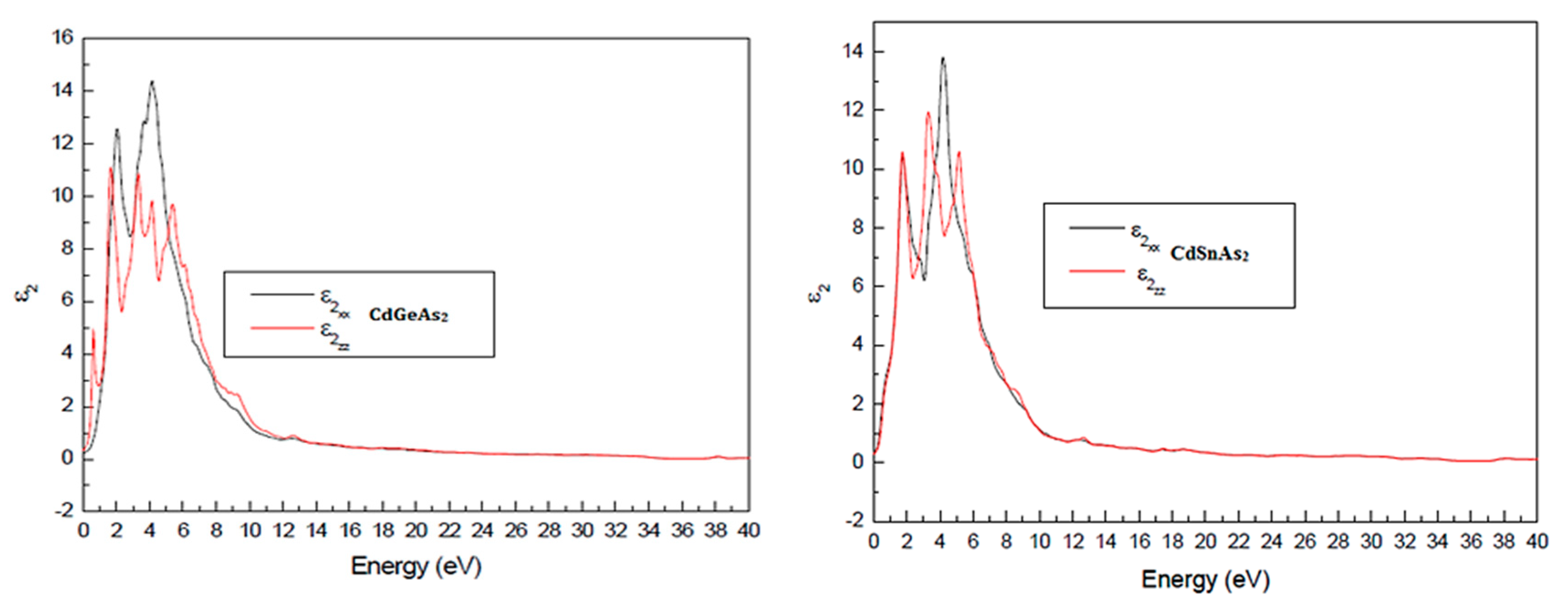
Figure 4: Imaginary part of the insulator function ε2(ω) for CdGeAs2 and CdSnAs2.
Subsequent peaks in ε2(ω) indicate higher-energy transitions involving secondary conduction or valence bands, reflecting a complex band structure with multiple critical points (e.g., M, Γ, Z) in the Brillouin zone.
3.3.6 Indexes Refraction and Extinction
Fig. 5 explains the photon-energy dependence of the refractive index n(ω) and the extinction coefficient k(ω). A modest yet noticeable optical anisotropy is observed, with Δn(0) values of 0.05 for CdSnAs2 and 0.02 for CdGeAs2, indicating that the velocity of light propagation slightly depends on the polarization direction. With increasing photon energy, the refractive index rises and attains its maximum within the visible range at 3.542 eV for CdSnAs2 and 3.589 eV for CdGeAs2, before gradually decreasing. This trend is characteristic of semiconducting materials and is associated with the saturation of electronic polarization at higher frequencies.
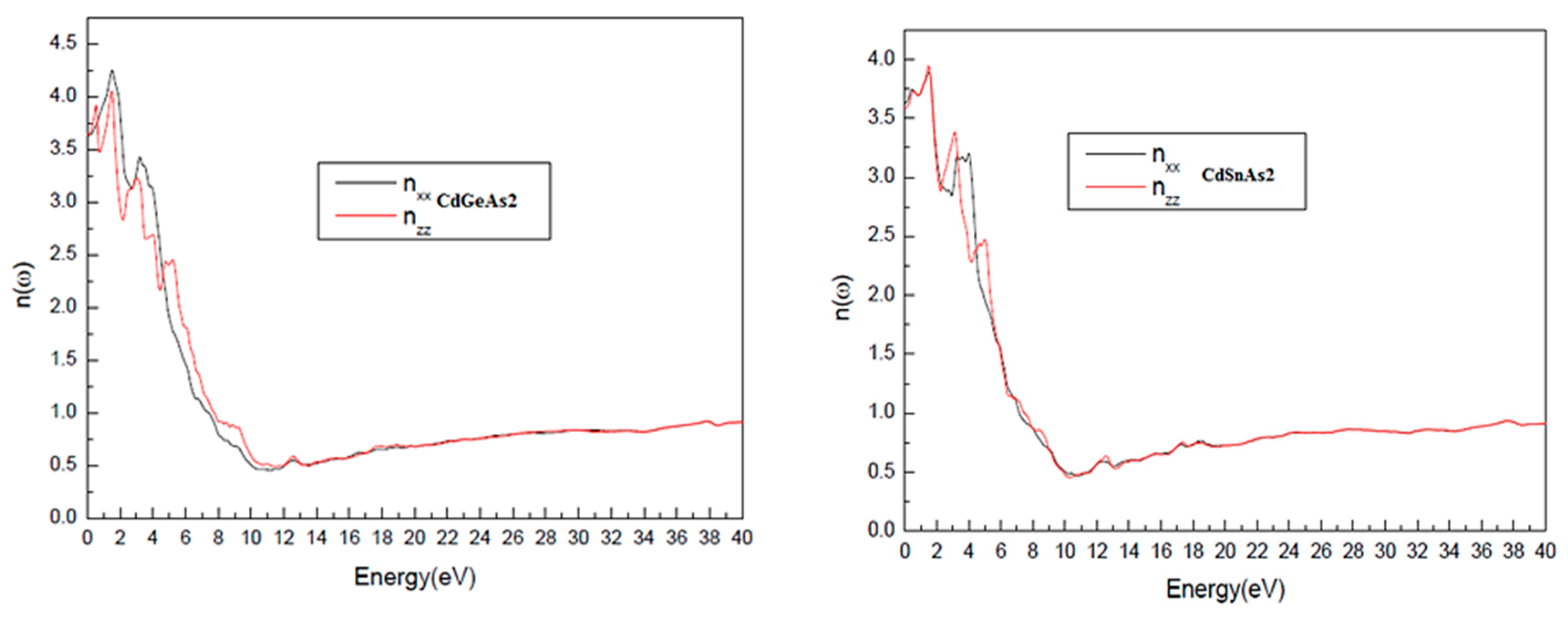
Figure 5: Refractive index n(ω) as a function of photon energy for CdGeAs2 and CdSnAs2.
The destruction coefficient k(ω), (Fig. 6) which measures the attenuation of the electromagnetic wave inside the material, exhibits a crowning at the energy where the real part of the insulator function crosses zero. This corresponds to plasma-type resonances, where absorption and dispersion are spectrally aligned. Beyond this critical energy, k(ω) decreases, indicating condensed optical sufferers at higher photon energies.
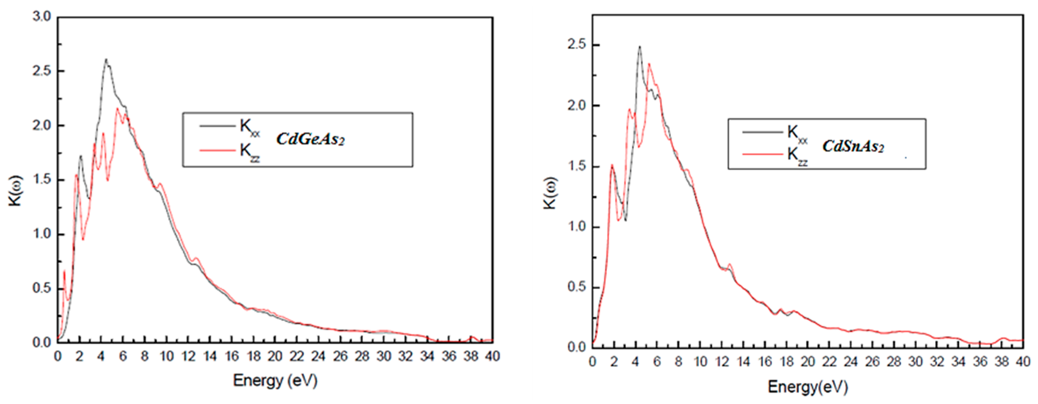
Figure 6: Variation of the Extinction Coefficient, k(ω) as a function of energy for CdGeAs2 and CdSnAs2.
The static limit of the dielectric constant ε1(0) and refractive index n(0) reflects the degree of electronic polarizability when no oscillating field is present. Table 3 lists these values, which show excellent agreement with theoretical data from the literature, thereby validating the present FP-LAPW approach. Beyond their fundamental significance, these quantities are essential in practical low-frequency technologies such as waveguides and optical modulators.
Table 3: Summary of zero-frequency optical parameters, including ε1(0) and n(0), for CdSnAs2 and CdGeAs2 compounds.
As depicted in Fig. 7, the optical reflectivity R(ω) attains its highest values within the ultraviolet energy region, spanning from 3.30 to 11.27 eV for CdGeAs2 and from 3.14 to 10.12 eV for CdSnAs2. These pronounced reflectivity levels are linked to increased values of the real part of the dielectric function, ε1(ω), which generate a strong refractive index mismatch between the material and the surrounding vacuum. At higher photon energies, a gradual reduction in reflectivity is observed, reflecting improved optical transparency and diminished reflection losses at the interface.
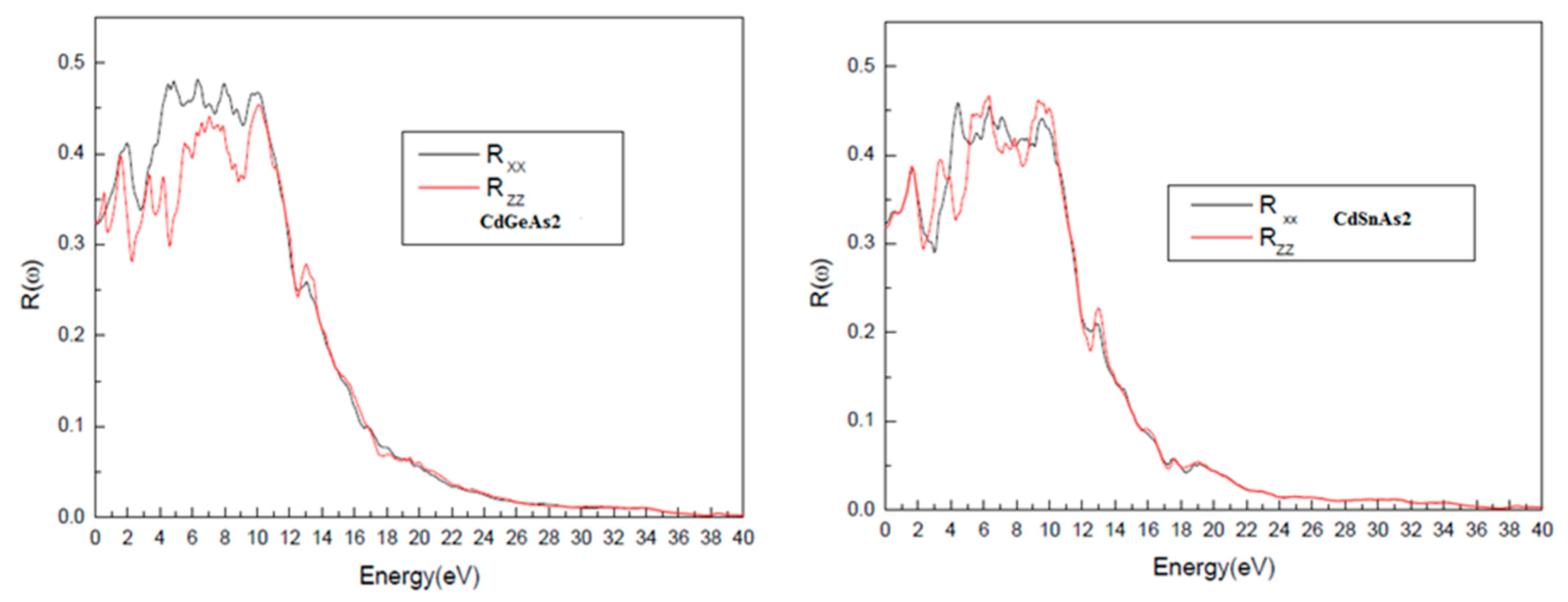
Figure 7: Energy-dependent of the optical reflectivity R(ω), for CdGeAs2 and CdSnAs2.
3.5 Absorption Coefficient and Mid-Infrared Transparency
The absorption coefficient α(ω), illustrated in Fig. 8, characterizes the material’s ability to attenuate the incident light intensity via internal absorption. The absorption onsets are located at 1.16 eV for CdGeAs2 and 1.12 eV for CdSnAs2, confirming the direct band-to-band nature of the fundamental transitions. As the photon energy increases beyond these edges, α(ω) rises sharply, then decreases at high energies due to the saturation of available electronic states.
Importantly, the near-zero values of α(ω) at low energies indicate that these compounds are transparent in the mid-infrared (MIR) region. This property is highly sought after in materials for infrared optics, photonic sensors, and thermal imaging applications.
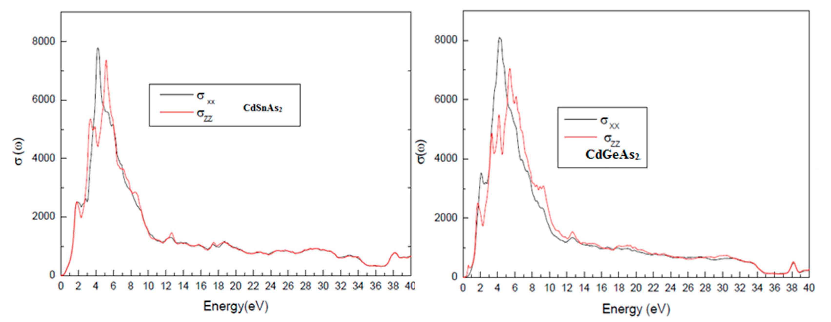
Figure 8: Energy-dependent variation of the absorption α(ω) for the for CdSnAs2 and CdGeAs2.
Fig. 9 displays the optical conductivity σ(ω), which describes the material’s ability to generate charge carriers in response to incident radiation. Optical conductivity is directly proportional to the number of photoexcited carriers, and therefore critical for assessing the photoelectric conversion efficiency. Both materials exhibit significant σ(ω) values in the visible range (1.65–3.1 eV), confirming their suitability as active layers in solar cells, especially in multi-junction or tandem architectures, where materials are selected to absorb different regions of the solar spectrum.
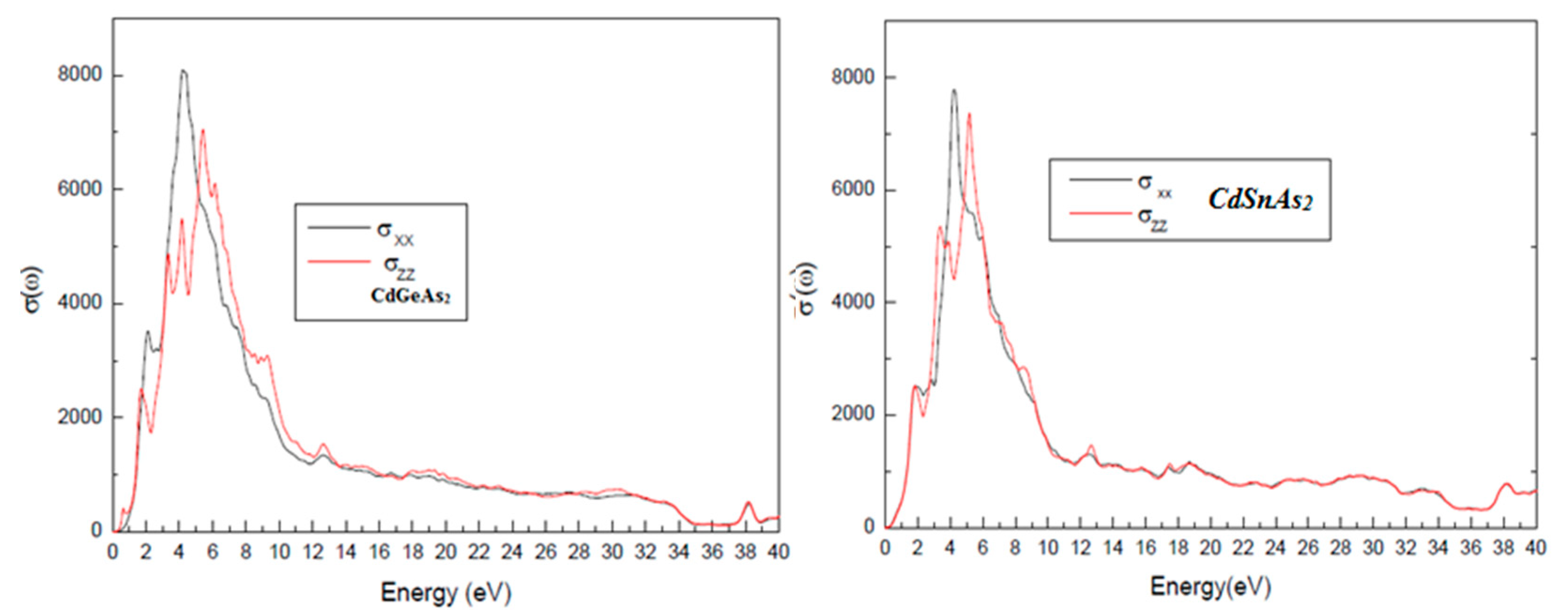
Figure 9: Optical conductivity spectra σ(ω) of CdGeAs2 and CdSnAs2 in the visible energy range.
Elastic characteristics are among the most critical indicators of crystalline materials, as they reveal insights into mechanical stability, resistance to deformation, and the fundamental nature of atomic interactions. These parameters can be accurately obtained through first-principles energy calculations, which analyze how the system’s total energy responds to slight distortions of the unit cell. To ensure reliable outcomes, the applied strains were carefully chosen to preserve, as much as possible, the inherent symmetry of the tetragonal crystal framework.
In tetragonal chalcopyrite-type structures, there are six independent elastic constants due to the symmetry of the lattice:
These parameters represent, in order: the longitudinal rigidity along the a- and c-axes, the coupling between the axial directions, and the shear resistance across different crystallographic planes.
The calculated values for
Table 4: Planned elastic constants Cij (GPa) for CdMAs2 (M = Sn, Ge) compounds in the chalcopyrite structure.
| | | | | | | ||
|---|---|---|---|---|---|---|---|
| | Our calculation | 57.0491 | 40.8252 | 41.3043 | 62.2741 | 18.1398 | 24.0859 |
| Outher calculation [23] | 69 | 44.6 | 45.5 | 63.2 | 19.7 | 23.7 | |
| Our calculation | 55.2031 | 41.0732 | 40.9276 | 53.0630 | 29.9953 | 21.0787 | |
| Outher calculation [26] | 63.4 | 43.6 | 54.20 | 71.40 | 22.4 | 23.0 | |
| [27] | 64.28 | 44.15 | 44.04 | 64.07 | 24.08 | 23.57 | |
| [28] | 78.3 | 49.0 | 57.3 | 90.4 | 33.2 | 30.1 | |
The following mechanical trends are observed:
For both compounds,
In
Conversely, in CdSnAs2,
The computed elastic constants fulfill the Born criteria for mechanical stability in tetragonal systems:
These criteria demonstrate that both materials are mechanically stable under equilibrium conditions. To evaluate the isotropic elastic response of polycrystalline systems, the bulk and shear moduli were estimated using the Voigt, Reuss, and Voigt–Reuss–Hill (VRH) averaging schemes, which provide representative macroscopic mechanical parameters.
The bulk modulus (B) characterizes the resistance of a material to volumetric compression under hydrostatic pressure, whereas the shear modulus (G) describes its opposition to shape deformation under applied shear stress. The Young’s modulus (Y) reflects the material stiffness in response to uniaxial loading, while the Poisson’s ratio (ν) represents the ratio between transverse contraction and longitudinal elongation under tensile deformation.
The employed equations are:
The moduli presented in Table 5 demonstrate strong consistency between the bulk modulus values derived from elastic constants and those obtained using the Murnaghan equation of state, thereby reinforcing the reliability of the mechanical analysis.
Physical Interpretation of Mechanical Behavior.
Brittleness via Ductility: Pugh’s Ratio (B/G).
The B/G ratio, introduced by Pugh, is a powerful indicator of the ductile or brittle nature of materials:
B/G > 1.75 → Ductile behavior (able to undergo plastic deformation).
B/G < 1.75 → Brittle behavior (tends to fracture upon stress).
In this study, both CdGeAs2 and CdSnAs2 exhibit B/G ratios greater than 1.75, suggesting that both materials are basically ductile. This is advantageous for fabrication processes and flexible device applications.
Bonding Character and Poisson’s Ratio (v).
Poisson’s ratio provides insight into the interatomic bonding nature:
v ≈ 0.1 → Dominant covalent bonding (e.g., diamond),
v ≈ 0.25 → Mainly ionic bonding,
v > 0.33 → Strong contribution from central forces (long-range electrostatic interactions).
In our case:
v ≈ 0.367 for CdGeAs2,
v ≈ 0.346 for CdSnAs2.
Table 5: Bulk modulus (GPa), shear modulus (GPa), Poisson’s ratio, and young’s modulus (GPa) for
| | | B (GPa) | | | | | | | |
|---|---|---|---|---|---|---|---|---|---|
| | 49.610 | 49.610 | 49.610 | 15.602 | 13.160 | 14.381 | 3.449 | 0.3678 | 39.3415 |
| Outher calculation [23] | 52 | 16 | 3.27 | 0.36 | 44 | ||||
| | 45.480 | 45.450 | 45.465 | 18.915 | 12.170 | 15.542 | 2.9252 | 0.346 | 41.85772 |
These values indicate an important ionic influence, consistent with the presence of Cd-As and Ge/Sn-As bonds, which exhibit strong electrostatic character. This ionic dominance aligns with the electronic structure of chalcopyrite-type semiconductors.
The Young’s modulus reflects the overall stiffness of the material in response to tensile forces. The values obtained confirm that both materials are moderately stiff, with CdGeAs2 showing slightly higher stiffness, which corresponds well with its lower in-plane compressibility.
From the above mechanical analysis, we conclude that both CdGeAs2 and CdSnAs2:
- Are mechanically stable and satisfy all elastic stability conditions,
- Exhibit moderate elastic anisotropy, influenced by the choice of metal cation,
- Possess ductile behavior, as predicted by Pugh’s criterion,
- Have predominantly ionic bonding character, with strong central-force interactions.
These mechanical features, combined with their promising optical and electronic properties, make these materials excellent candidates for optoelectronic, infrared sensing, and photovoltaic applications, especially in environments where mechanical robustness and ductility are required.
This research presents an ab initio investigation of CdGeAs2 and CdSnAs2 chalcopyrite semiconductors, focusing on their operational, optical, electronic, elastic, and thermoelectric characteristics. The simulations were conducted using the FP-LAPW approach within the DFT framework. Structural parameters for the ternary systems and their alloys were derived with the WC-GGA functional, whereas the electronic band gaps were determined using the modified Becke–Johnson (mBJ) potential, available in the recent WIEN2k release.
For both ternary compounds, the predicted lattice constants, the c/a ratio, the internal coordinate u, and the bulk modulus show strong consistency with informed theoretical and experimental values. Band structure calculations confirmed that CdGeAs2 and CdSnAs2 are direct-gap semiconductors with the gap positioned at the Γ point. As anticipated, WC-GGA underestimated the band gap relative to experimental data, whereas the mBJ potential produced values much closer to the measured results, validating its reliability for accurate prediction of semiconductor electronic properties.
The optical behavior of these chalcopyrite compounds was also examined. Calculations of the real and imaginary parts of the dielectric function, together with refractive index, reflectivity, and absorption coefficient, were carried out. At zero frequency, the dielectric constants matched previously published values, whereas other optical indicators are provided as predictions in the absence of experimental references. Examination of ε1(ω) and ε2(ω) demonstrated that CdGeAs2 and CdSnAs2 become optically isotropic above 10 eV, with only weak anisotropy persisting below this energy range.
Reflectivity spectra showed pronounced reflection in the ultraviolet range, extending from about 3.30–11.27 eV for CdGeAs2 and 3.14–10.12 eV for CdSnAs2. The evaluated elastic constants confirmed mechanical stability in both materials. Derived mechanical moduli further indicated ductile behavior, with bonding dominated by ionic interactions.
Acknowledgement:
Funding Statement: The authors received no specific funding for this study.
Author Contributions: The authors confirm their contributions to this manuscript as follows: conceptualization and study design, Khaled Lazar, Y. Megdoud, and A. Boukhari; methodology and computational implementation, Khaled Lazar and R. Meneceur; data analysis and interpretation, M. Laouamer, Y. Yahiaoui, and Y. Benkrima; validation and formal analysis, A. Achour and Y. Megdoud; manuscript drafting, Khaled Lazar and M. Laouamer; manuscript review and editing, all authors. All authors reviewed and approved the final version of the manuscript.
Availability of Data and Materials: The data supporting the findings of this study are available within the article. Additional data may be obtained from the corresponding author (Y. Megdoud and Y. Benkrima) upon reasonable request.
Ethics Approval: Not applicable.
Conflicts of Interest: The authors declare no conflicts of interest.
References
1. Delgado-Montiel T , Soto-Rojo R , Soto-Acosta S , Peñuelas CA , Ruelas-Ávila ME , Baez-Castro A , et al. DFT/TD-DFT studies on carbazole-diphenylamine-based dyes using different π-bridges for DSSCs. Struct Chem. 2025. doi:10.1007/s11224-025-02597-1. [Google Scholar] [CrossRef]
2. Teng J , Chen X , Gao H , Huangfu K , Wu S , Ma Z , et al. Photovoltaic microorganism hybrid systems for enhanced polyhydroxybutyrate synthesis through material design and energy mass transfer mechanisms. Materials. 2025; 19( 1): 1. doi:10.3390/ma19010001. [Google Scholar] [CrossRef]
3. Megdoud Y , Tairi L , Benkrima Y , Meneceur R , Lakel A , Ghemid S , et al. First-principles predictions: Exploring semiconductor properties of BeXAs2 (X=Ge and Sn) for photovoltaic applications. J Ovonic Res. 2024; 20( 4): 435– 43. doi:10.15251/JOR.2024.204.435. [Google Scholar] [CrossRef]
4. Wei S-H , Zunger A . Band offsets and optical bowings of chalcopyrites and Zn-based II-VI alloys. Appl Phys Lett. 1988; 78( 6): 3846– 56. doi:10.1063/1.359901. [Google Scholar] [CrossRef]
5. Siebentritt S , Rau U . Wide-Gap Chalcopyrites. Berlin/Heidelberg, Germany: Springer; 2006. doi:10.1007/b105644. [Google Scholar] [CrossRef]
6. Chiker F , Abbar B , Tadjer A , Bresson S , Khelifa B , Mathieu C . Electronic structure and optical properties of ternary CdXP2 semiconductors (X=Si, Ge and Sn) under pressure. Phys B Condens Matter. 2004; 349( 1–4): 181– 91. doi:10.1016/j.physb.2004.03.087. [Google Scholar] [CrossRef]
7. Chiker F , Abbar B , Bresson S , Khelifa B , Mathieu C , Tadjer A . The reflectivity spectra of ZnXP2 (X=Si, Ge, and Sn) compounds. J Solid State Chem. 2004; 177( 11): 3859– 67. doi:10.1016/j.jssc.2004.07.020. [Google Scholar] [CrossRef]
8. Kocak B , Ciftci YO . Ab-initio calculations of semiconductor MgGeP2 and MgGeAs2. Mater Res Bull. 2016; 77: 300– 6. doi:10.1016/j.materresbull.2016.02.008. [Google Scholar] [CrossRef]
9. Marfaing Y . Énergie photovoltaïque: Matériaux utilisés et perspectives. J Phys IV France. 2002; 12( 2): 145– 54. doi:10.1051/jp420020021. [Google Scholar] [CrossRef]
10. Müller J , Nowoczin J , Schmitt H . Composition, structure and optical properties of sputtered thin films of CuInSe2. Thin Solid Films. 2006; 496( 2): 364– 70. doi:10.1016/j.tsf.2005.09.077. [Google Scholar] [CrossRef]
11. Gupta RC , Varshney P , Pravesh , Lal M , Kumar D , Singh K , et al. Mechanical stability parameters of chalcogenides and pnictides based optoelectronic materials. Chalcogenide Lett. 2023; 20( 2): 101– 12. doi:10.15251/CL.2023.202.101. [Google Scholar] [CrossRef]
12. Xue S , Ning J , Zhang B , Wu Q , Zhang F , Zhang W . The electronic structure and optical properties of CdGeAs2 crystal: A DFT and HSE06 study. Coatings. 2022; 12( 11): 1778. doi:10.3390/coatings12111778. [Google Scholar] [CrossRef]
13. Plata JJ , Posligua V , Márquez AM , Fernandez Sanz J , Grau-Crespo R . Charting the lattice thermal conductivities of I–III–VI2 chalcopyrite semiconductors. Chem Mater. 2022; 34( 6): 2833– 41. doi:10.1021/acs.chemmater.2c00336. [Google Scholar] [CrossRef]
14. Laouamer M , Megdoud Y , Remha S , Mahmoudi A , Adaika M , Benkrima Y , et al. Ab initio investigation of the structural, electronic, optical, and thermoelectric properties of absorber materials AuAlS2 and AuInS2 for enhanced solar panel efficiency. J Ovonic Res. 2025; 21( 6): 741– 59. doi:10.15251/JOR.2025.216.741. [Google Scholar] [CrossRef]
15. Meneceur N , Megdoud Y , Meneceur R , Boukhari A , Benkrima Y , Tairi L , et al. Theoretical study of physical characterization of ScP and ScAs binary compounds and their ternary alloy ScP1-xAsx: Wien2K code. Dig J Nanomater Biostruct. 2025; 20( 4): 1487– 98. doi:10.15251/DJNB.2025.204.1487. [Google Scholar] [CrossRef]
16. Yu M , Xiao X , Xiong Z , Li J , Liu X , Huang W , et al. Structural, electronic and optical properties of CdGeAs2 with hybrid density functional (HSE06). Mater Today Commun. 2022; 31: 103276. doi:10.1016/j.mtcomm.2022.103276. [Google Scholar] [CrossRef]
17. Yu Y , Zhao B , Zhu S , Gao T , Hou H , He Z . Ab initio study of the linear and nonlinear optical properties of chalcopyrite CdGeAs2. J Solid State Chem. 2012; 185: 264– 70. doi:10.1016/j.jssc.2011.10.014. [Google Scholar] [CrossRef]
18. Madsen GKH , Blaha P , Schwarz K , Sjöstedt E , Nordström L . Efficient linearization of the augmented plane-wave method. Phys Rev B. 2001; 64( 19): 195134. doi:10.1103/PhysRevB.64.195134. [Google Scholar] [CrossRef]
19. Schwarz K , Blaha P , Madsen GKH . Electronic structure calculations of solids using the WIEN2k package for material sciences. Comput Phys Commun. 2002; 147( 1–2): 71– 6. doi:10.1016/S0010-4655(02)00206-0. [Google Scholar] [CrossRef]
20. Wu Z , Cohen RE . More accurate generalized gradient approximation for solids. Phys Rev B. 2006; 73( 23): 235116. doi:10.1103/PhysRevB.73.235116. [Google Scholar] [CrossRef]
21. Tran F , Laskowski R , Blaha P , Schwarz K . Performance on molecules, surfaces, and solids of the Wu-Cohen GGA exchange-correlation energy functional. Phys Rev B. 2007; 75( 11): 115131. doi:10.1103/PhysRevB.75.115131. [Google Scholar] [CrossRef]
22. Tran F , Blaha P . Accurate band gaps of semiconductors and insulators with a semilocal exchange-correlation potential. Phys Rev Lett. 2009; 102( 22): 226401. doi:10.1103/PhysRevLett.102.226401. [Google Scholar] [CrossRef]
23. Touat D , Ferhat M , Zaoui A . Dynamical behaviour in the boron III–V group: A first-principles study. J Phys Condens Matter. 2006; 18( 15): 3647– 54. doi:10.1088/0953-8984/18/15/011. [Google Scholar] [CrossRef]
24. Koubil A , Khettal M , Megdoud Y , Laouamer M , Benkrima Y , Tairi L , et al. Advanced first-principle study of AgGaTe2 and AgInTe2 chalcopyrite semiconductors: Structural, electronic, and optical properties via FPLAPW within WIEN2K. East Eur J Phys. 2025;( 4): 427– 34. doi:10.26565/2312-4334-2025-4-42. [Google Scholar] [CrossRef]
25. Moss TS . A relationship between the refractive index and the infra-red threshold of sensitivity for photoconductors. Proc Phys Soc Sect B. 1950; 63( 3): 167. doi:10.1088/0370-1301/63/3/302. [Google Scholar] [CrossRef]
26. Ingram JC , Nebesny KW , Pemberton JE . Optical properties of selected first-row transition metals determined by reflection electron energy loss spectroscopy. Appl Surf Sci. 1990; 45( 3): 247– 56. doi:10.1016/0169-4332(90)90007-M. [Google Scholar] [CrossRef]
27. Ghosh A , Thangavel R , Rajagopalan M . Electronic and optical modeling of solar cell compound CuXY2 (X=In, Ga, Al; Y=S, Se, Te): First-principles study via Tran–Blaha-modified Becke–Johnson exchange potential approach. J Mater Sci. 2015; 50( 4): 1710– 7. doi:10.1007/s10853-014-8732-z. [Google Scholar] [CrossRef]
28. Ohmer MC , Goldstein JT , Zelmon DE , Saxler AW , Hegde SM , Wolf JD , et al. Infrared properties of AgGaTe2, a nonlinear optical chalcopyrite semiconductor. J Appl Phys. 1999; 86( 1): 94– 9. doi:10.1063/1.370704. [Google Scholar] [CrossRef]
29. Aroudj M , Megdoud Y , Laouamer M , Meneceur R , Khadem M , Benkrima Y . Density functional theory analysis of structural and electronic properties of IV–VI semiconductors: PbSe, PbS, and PbSe1−xSx alloys. Int J Comput Exp Sci Eng. 2025; 11( 4): 7887– 96. doi:10.22399/ijcesen.4164. [Google Scholar] [CrossRef]
30. Salehi H , Gordanian E . Ab initio study of structural, electronic and optical properties of ternary chalcopyrite semiconductors. Mater Sci Semicond Process. 2016; 47: 51– 6. doi:10.1016/j.mssp.2016.02.015. [Google Scholar] [CrossRef]
31. Reddy RR , Nazeer Ahammed Y , Rama Gopal K , Raghuram DV . Optical electronegativity and refractive index of materials. Opt Mater. 1998; 10( 2): 95– 100. doi:10.1016/S0925-3467(97)00171-7. [Google Scholar] [CrossRef]
32. Cui S , Feng W , Hu H , Feng Z , Wang Y . First principles studies of phase stability, electronic and elastic properties in BBi compound. Comput Mater Sci. 2010; 47( 4): 968– 72. doi:10.1016/j.commatsci.2009.11.030. [Google Scholar] [CrossRef]
33. Ravindra NM , Ganapathy P , Choi J . Energy gap–refractive index relations in semiconductors–An overview. Infrared Phys Technol. 2007; 50( 1): 21– 9. doi:10.1016/j.infrared.2006.04.001. [Google Scholar] [CrossRef]
Cite This Article
 Copyright © 2026 The Author(s). Published by Tech Science Press.
This work is licensed under a Creative Commons Attribution 4.0 International License , which permits unrestricted use, distribution, and reproduction in any medium, provided the original work is properly cited.
 Downloads
 Citation Tools