
 Submit a Paper
 Propose a Special lssue
 Open Access
ARTICLE

High-Efficiency Double-Heterojunction Based Dual-Absorber Perovskite Solar Cell via Numerical Optimization
Department of Physics, Aljamoum University College, Umm Al-Qura University, Makkah, Saudi Arabia
* Corresponding Author: Soheib Dakhelullah Alsahafi. Email:
Chalcogenide Letters 2026, 23(3), 2 https://doi.org/10.32604/cl.2026.077336
Received 07 December 2025; Accepted 25 February 2026; Issue published 03 April 2026
 View Full Text
 Download PDF
Abstract
In this study, a novel double-heterojunction perovskite solar cell (DHPSC) with the following structure: FTO/ZnO/CH3NH3PbI3−xClx/CH3NH3SnI3/p++ZnTe/Au was designed. It was optimized using the wxAMPS simulation software. A systematic parametric analysis was performed to investigate the influence of electron transport layer (ETL) ZnO and hole transport layer (HTL) thicknesses on photovoltaic performance. That includes short-circuit current density (Jsc), open-circuit voltage (Voc), fill factor (FF), and power conversion efficiency (η). The results indicate that once a minimum ZnO thickness is achieved, further increases have a negligible effect on performance. Whereas variations in ZnTe thickness markedly influence Voc and η. The optimal configuration obtained, comprising a FTO (200 nm)/ZnO (600 nm)/CH3NH3PbI3−xClx (800 nm)/CH3NH3SnI3 (800 nm)/ZnTe (350 nm), achieved a Voc of 1.996 V, Jsc of 20.61 mA/cm2, FF of 93.11%, and 38.24%. Quantum efficiency analysis revealed superior spectral response, exceeding 95% across the visible spectrum. These findings demonstrate the potential of a thickness-optimized DHPSC device for achieving high performance, providing a pathway for future experimental validation and fabrication.Keywords
Over the past decade, perovskite solar cells (PSCs) have emerged as one of the most promising photovoltaic technologies due to their remarkable power conversion efficiencies. They also offer low production costs and flexible material properties [1,2,3]. Since their first demonstration in 2009 with an efficiency of around 3.8% [4], PSCs have undergone rapid advancements. They now achieve over 25% efficiency in single-junction configurations [5]. However, challenges such as stability under ambient conditions and toxicity related to lead-based materials. In addition, charge recombination losses are present. These issues still hinder their commercialization [6,7,8]. To address these issues, researchers have focused on modifying the architecture of PSCs. This approach aims to further enhance device performance. Heterojunction engineering has been considered a possible solution. Introducing different semiconductor layers with matching properties can significantly improve charge carrier separation. It can suppress recombination and facilitate more efficient charge transport. Accordingly, the use of double heterojunctions, in which two absorber layers are stacked with tailored band alignments, has shown potential to boost overall efficiency. This is achieved by broadening the absorption spectrum and optimizing internal electric fields [9,10].
Recent advances in perovskite solar cells (PSCs) have focused on tandem architectures, interface engineering, and novel charge transport materials to push power conversion efficiencies (PCEs) beyond 30%. Significant progress has been made in understanding recombination dynamics, tunneling mechanisms, and absorber heterostructuring [11]. However, ZnO/perovskite interfaces with atomic-layer-deposited interlayers, demonstrating that surface hydroxyl-group passivation reduces trap-assisted recombination and improves PCE. Additional studies have highlighted the role of heavily doped inorganic HTLs (e.g., p++CuI, p++NiOx) in reducing series resistance and enabling high fill factors in all-perovskite tandems [12].
Despite these advances, a critical research gap remains: limited experimental and simulated validation of monolithic all-perovskite tandem cells employing a double-heterojunction architecture with ZnO as the ETL and heavily doped p++ZnTe as the HTL, particularly regarding the interplay between band alignment, tunneling losses, and carrier extraction under calibrated material parameters. Most reported high-efficiency tandems rely on organic or metal-oxide recombination layers, while the potential of ZnTe—a high mobility, stable, inorganic p-type semiconductor—remains underexplored in perovskite photovoltaics.
Among the commonly studied perovskite materials, methylammonium lead mixed halide (CH3NH3PbI3−xClx) has gained attention for its improved film quality, enhanced crystallinity, and better environmental stability compared to CH3NH3PbI3 alone [13,14]. Incorporating chlorine into the perovskite structure results in larger grain sizes and reduced trap states, contributing to improved device performance. Experimental studies have reported PCEs exceeding 16–18% with CH3NH3PbI3−xClx, along with enhancements in open-circuit voltage and device reproducibility [15,16,17].
On the other hand, methylammonium tin iodide (CH3NH3SnI3) represents a promising lead-free alternative with strong light absorption properties, particularly in the nearinfrared region [18,19]. While tin-based perovskites are more environmentally friendly, they suffer from intrinsic instability due to the oxidation of Sn2+ to Sn4+, which can lead to p-type self-doping and performance degradation [20,21]. Nonetheless, recent studies using interface passivation, optimized transport layers, and careful control of the fabrication environment have shown meaningful improvements in both stability and efficiency of CH3NH3SnI3-based devices [22,23].
Combining materials such as CH3NH3PbI3−xClx and CH3NH3SnI3 in multi-absorber designs enables harnessing the advantages of both wide- and narrow-bandgap absorbers while minimizing their respective drawbacks. This multi-absorber approach has been supported by both experimental and simulation studies as a viable route to pushing the efficiency limits of PSCs beyond what is possible with conventional single-junction devices [24].
By bridging the gap between advanced inorganic transport layers (ZnO/p++ZnTe) and low-loss tandem perovskite absorbers, this study provides a pathway toward stable, high-efficiency, hysteresis-free photovoltaics suitable for next-generation applications, including building-integrated and automotive-integrated PV systems.
2 Simulation Framework and Numerical Model
Numerical modeling was performed using wxAMPS (Analysis of Microelectronic and Photonic Structures), an advanced solar cell simulation platform that extends the original AMPS code to include intra-band tunneling and trap-assisted tunneling, which are critical for accurate modeling of heterojunction and tunnel-junction interfaces [25,26,27].
wxAMPS solves the coupled semiconductor equations in one dimension: Poisson’s equation for electrostatic potential, relating local charge densities from free carriers, dopants, and traps; electron and hole continuity equations under the drift-diffusion model, accounting for carrier generation, recombination, and transport under electric fields; recombination mechanisms including Shockley-Read-Hall (SRH), direct, and Auger processes; and tunneling transport models for intra-band and trap-assisted tunneling across energy barriers [25,28].
Material parameters, including thicknesses, band gaps (Eg), electron affinities (χ), hole mobilities (μp), electron mobilities (μn), dielectric permittivity (ε), donor density (Nd), acceptor density (Na), conduction band effective density of states (Nc), valence band effective density of states (Nv). The parameter values for various materials are detailed in Table 1 and were sourced from recent literature or previous calibration [29,30,31,32,33,34,35]. Simulations were conducted under AM 1.5G illumination (100 mW cm−2) at 300 K.
The simulation generated J-V curves (illuminated and dark) for extracting Voc, Jsc, fill factor (FF), and power conversion efficiency (η); energy band diagrams showing conduction/valence band profiles, quasi-Fermi levels, and interface offsets; quantum efficiency (QE) spectra for wavelength-dependent current generation; and parametric sweeps for thickness, doping, and defect density to identify optimal configurations.
This modeling framework enabled detailed evaluation of the electrical and optical performance of the proposed PSC, providing insight into how material properties and interface characteristics influence overall device efficiency without the need for extensive experimental fabrication.
In this investigation, the double-heterojunction perovskite solar cell (PSC) was modeled using wxAMPS simulation software. The device structure, FTO/ZnO/CH3NH3PbI3−xClx/CH3NH3SnI3/p++ZnTe/Au, is illustrated in Fig. 1. This novel architecture employs CH3NH3PbI3−xClx as the primary absorber layer and CH3NH3SnI3 as the secondary absorber. The ZnO layer serves as the electron transport layer (ETL), while the highly doped ZnTe functions as the hole transport and tunnel-junction layer. The FTO layer is used as the transparent conductive oxide (TCO).
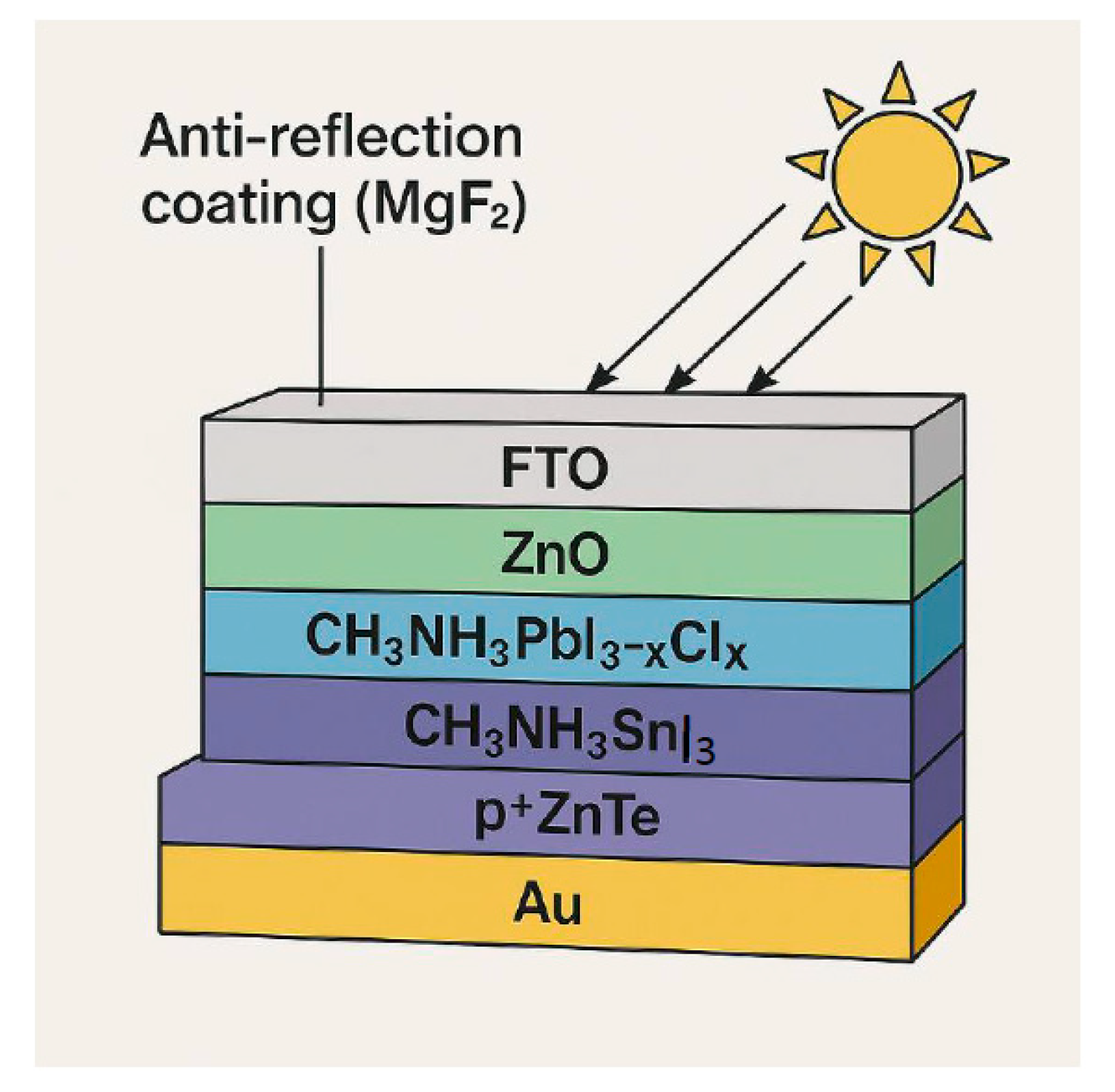
Figure 1: Schematic diagram of the simulated solar cell structure.
Table 1: The electric parameters sitting for the simulated solar cell used in the wxAMPS.
| Parameter | FTO | ZnO | CH3NH3PbI3−xClx | CH3NH3SnI3 | p++ZnTe |
|---|---|---|---|---|---|
| d (nm) | 200 | 100–800 | 800 | 800 | 100–350 |
| Eg (eV) | 3.6 | 3.3 | 1.55 | 1.3 | 2.26 |
| ε | 9 | 9 | 30 | 8.5 | 9.67 |
| χ (eV) | 4 | 4.4 | 3.9 | 4.17 | 3.5 |
| Nc (cm−3) | 2.2 × 10¹⁸ | 2.2 × 10¹⁸ | 2.2 × 10¹⁸ | 1 × 10¹⁸ | 7 × 10¹⁶ |
| Nv (cm−3) | 1.8 × 10¹⁹ | 1.8 × 10¹⁹ | 1.8 × 10¹⁹ | 1 × 10¹⁸ | 2 × 10¹⁹ |
| μe (cm2/V·s) | 20 | 100 | 2 | 1.6 | 330 |
| μh (cm2/V·s) | 10 | 25 | 2 | 1.6 | 80 |
| Nd (cm−3) | 2 × 10¹⁹ | 1 × 10¹⁸ | 1 × 10¹³ | - | - |
| Na (cm−3) | - | - | 1 × 10¹² | 1 × 10¹⁶ | 1 × 10²⁰ |
| Nt (cm−3) | - | 1 × 10¹⁵ | 5 × 10¹⁵ | 2 × 10¹⁶ | 1 × 10¹⁶ |
ZnO has a wide bandgap ~3.3 eV with a conduction band minimum (CBM) around ≈−4.4 eV (vs. vacuum) and a valence band maximum (VBM) near −7.7 eV. The perovskite CH3NH3PbI3 (MAPbI3) has a CBM of approximately ≈ −3.9 to −4.0 eV and a VBM of ≈ −5.4 eV. The Cl-containing variant typically exhibits a slightly higher (more negative) CBM, improving electron injection into ZnO.
The CBM of ZnO lies lower (more negative) than that of the perovskite, creating a favorable energy gradient for electron extraction. This minimizes interfacial recombination and enhances electron collection at the FTO cathode. Additionally, ZnO offers a high electron mobility of 10–100 cm2/V·s, supporting efficient charge transport. ZnTe is a p-type semiconductor with a bandgap of ~2.26 eV. Its VBM is around ≈−5.2 to −5.4 eV, and its CBM is about ≈−7.5 eV. Tin-based perovskite CH3NH3SnI3 has a narrower bandgap (~1.2–1.4 eV), with a VBM of ≈ −5.0 to −5.2 eV, and a CBM of ≈−3.8 eV. Thus, the VBM of p++ZnTe aligns well (slightly deeper) with the VBM of CH3NH3SnI3, enabling efficient hole extraction.
The small offset (<0.2–0.3 eV) between the perovskite VBM and ZnTe VBM provides a low-barrier pathway for holes while blocking electrons (due to large CBM mismatch), acting as an effective hole-selective contact. Heavy p-doping reduces series resistance and improves ohmic contact with the Au back electrode.
Compared to organic HTLs (e.g., spiro-OMeTAD), inorganic ZnTe offers better stability, higher hole mobility, and tunable doping, making it suitable for all-inorganic or hybrid tandem cells. Thus, ZnO and p++ZnTe are strategically chosen to provide type-I (staggered) band alignment with their adjacent perovskite layers, enabling selective extraction of electrons and holes, minimizing recombination, and supporting high photovoltaic performance in this multi-absorber architecture.
The structure of a perovskite solar cell is configured. To optimize the performance of the simulated solar cell structure, it’s crucial to ensure that the layer thicknesses are at their optimal values. These layer thicknesses influence the photovoltaic performance. Therefore, we investigated the effects of ZnO-ETL and ZnTe-HTL thicknesses on various solar cell performance parameters. These parameters include Jsc, Voc, FF, and η. The thicknesses of the ETL and HTL vary from 100 nm to 800 nm with stepping of 50 nm. At the same time, the thickness of the two absorber layers was fixed at 800 nm for each.
4.1 Effect of ZnO-ETL Thickness on Device Performance
Fig. 2 shows how the photovoltaic parameters (Voc, Jsc, FF, and η) change as the ZnO electron transport layer (ETL) thickness increases from 100 nm to 800 nm in steps of 50 nm, while the absorber layers CH3NH3PbI3−xClx and CH3NH3SnI3 are fixed at 800 nm each, FTO at 200 nm, and ZnTe at 100 nm.
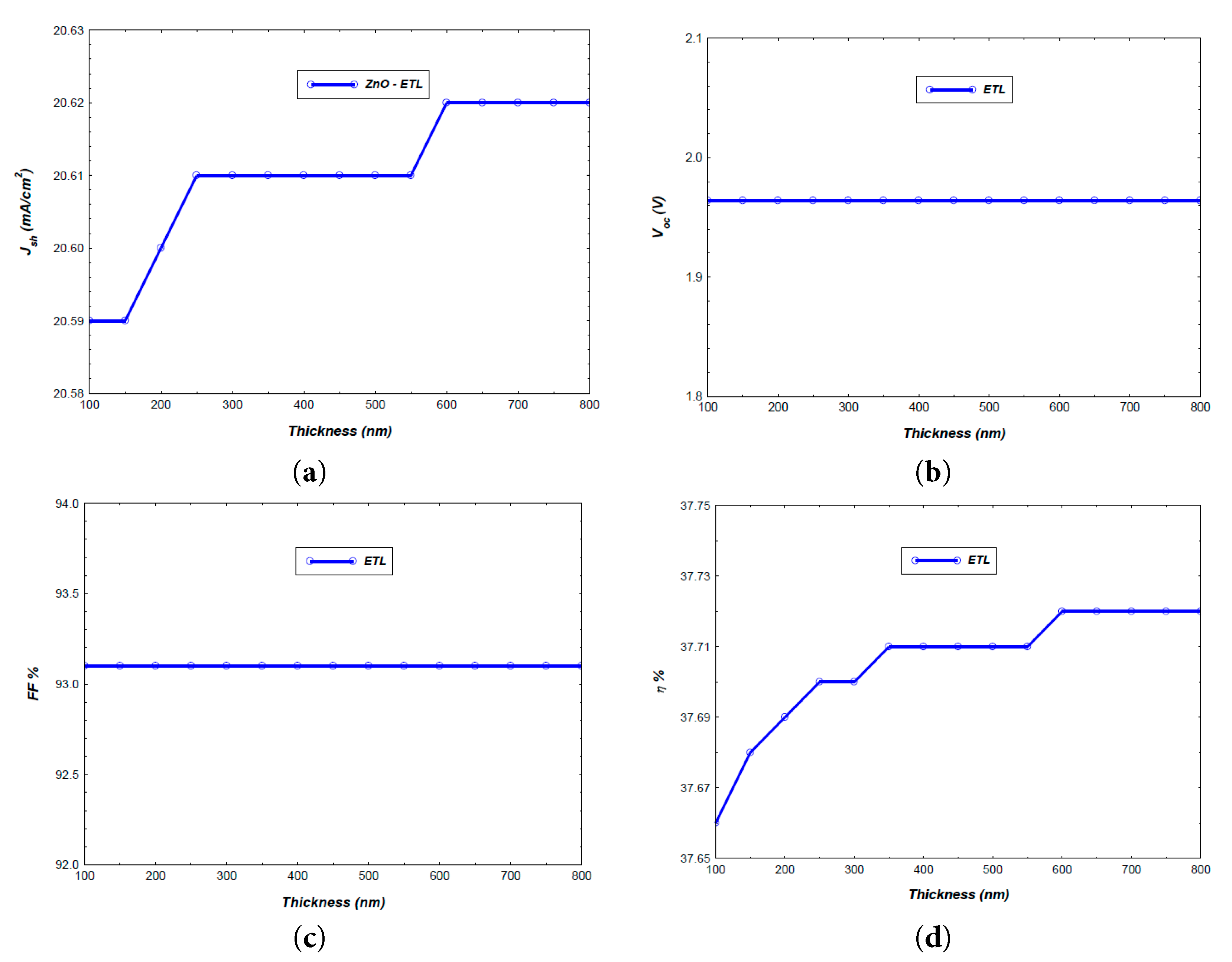
Figure 2: The obtained solar cell performance versus the ZnO-ETL thickness: (a) Jsc, (b) Voc, (c) FF, and (d) η.
The (Jsc) shows only a marginal increase from 20.59 mA/cm2 at 100 nm to 20.62 mA/cm2 at 800 nm, as illustrated in Fig. 2a. The slight improvement is likely due to minor reductions in resistive losses or small optical effects, but the variation is too small to be considered significant. In contrast, the results reveal that (Voc) remained constant at 1.964 V across the entire thickness range, as shown in Fig. 2b, indicating that ZnO thickness has a negligible impact on the built-in potential under the simulated conditions. This suggests that interface energetics and absorber properties dominate Voc rather than ETL thickness.
The (FF) remains stable at approximately 93.1% across all thicknesses. Otherwise, the (η) followed the trend of Jsc, increasing marginally from 37.66% at 100 nm to 37.72% at 800 nm, as shown in Fig. 2c,d. The extremely small variation < 0.06% absolute change confirms that ZnO thickness beyond a certain minimum (350 nm) has little influence on overall device performance.
The reported open-circuit voltage (Voc ≈ 2.0 V) and fill factor (FF > 93%) may initially appear unusually high for conventional single-junction perovskite solar cells, which typically exhibit Voc values below 1.2 V and FFs in the range of 75–85%. However, these values become physically plausible in the context of the tandem (or multi-absorber) architecture employed in this work. The device integrates two perovskite subcells with complementary bandgaps approximately 1.55–1.60 eV for CH3NH3PbI3−xClx and 1.2–1.3 eV for CH3NH3SnI3. In a properly connected two-terminal tandem configuration, the total Voc is expected to be close to the sum of the individual subcell Voc values (typically ~0.95–1.10 V for the wide-gap cell and ~0.75–0.85 V for the narrow-gap cell), yielding a combined Voc in the range of 1.7–1.95 V. A value near 2.0 V, while at the upper end, is not implausible under optimized conditions (e.g., low non-radiative recombination, excellent interfacial passivation, and balanced photocurrent).
Similarly, a fill factor exceeding 93% is rare but has been reported in high-performance tandem cells, particularly those with low series resistance, high shunt resistance, and minimal carrier recombination losses at interlayers [9,36].
The use of highly conductive, heavily doped p++ZnTe and high-mobility ZnO likely contributes to reduced resistive losses, while the graded perovskite heterojunction may suppress interface recombination.
In the proposed device architecture, the electron transport layer (ETL) based on ZnO exhibits negligible dependence on thickness once it exceeds a minimum threshold of approximately 350–600 nm. Below this range, incomplete surface coverage of the FTO substrate leads to shunting paths and reduced electron extraction efficiency. However, for thicknesses ≥ 350 nm, the ZnO film forms a continuous, pinhole-free layer that fully covers the underlying FTO, ensuring efficient electron collection and effective hole blocking.
Physically, this behavior arises because ZnO functions primarily as a charge-selective contact, not a light-absorbing layer. Once the film is thick enough to prevent direct contact between the perovskite and FTO (which would cause recombination and leakage), further increases in thickness do not significantly alter device performance provided the material maintains high crystallinity and low defect density. Additionally, ZnO’s high electron mobility (~10–100 cm2V−1s−1) ensures that even relatively thin layers can transport extracted electrons efficiently to the electrode without introducing substantial series resistance.
Thus, the minimum effective thickness is ~350 nm, dictated by the need for morpho-logical continuity and interfacial isolation rather than optical or transport limitations. However, a thickness of 600 nm provides good device efficiency, making it the recommended standard for optimal performance.
4.2 Effect of ZnTe-HTL Thickness on Device Performance
Fig. 3 presents the variation of key photovoltaic parameters as the ZnTe hole-transport layer (HTL) thickness was varied from 100 nm to 350 nm in steps of 50 nm, while keeping the CH3NH3PbI3−xClx and CH3NH3SnI3 absorber layers fixed at 800 nm each, FTO at 200 nm, and ZnO at 100 nm.
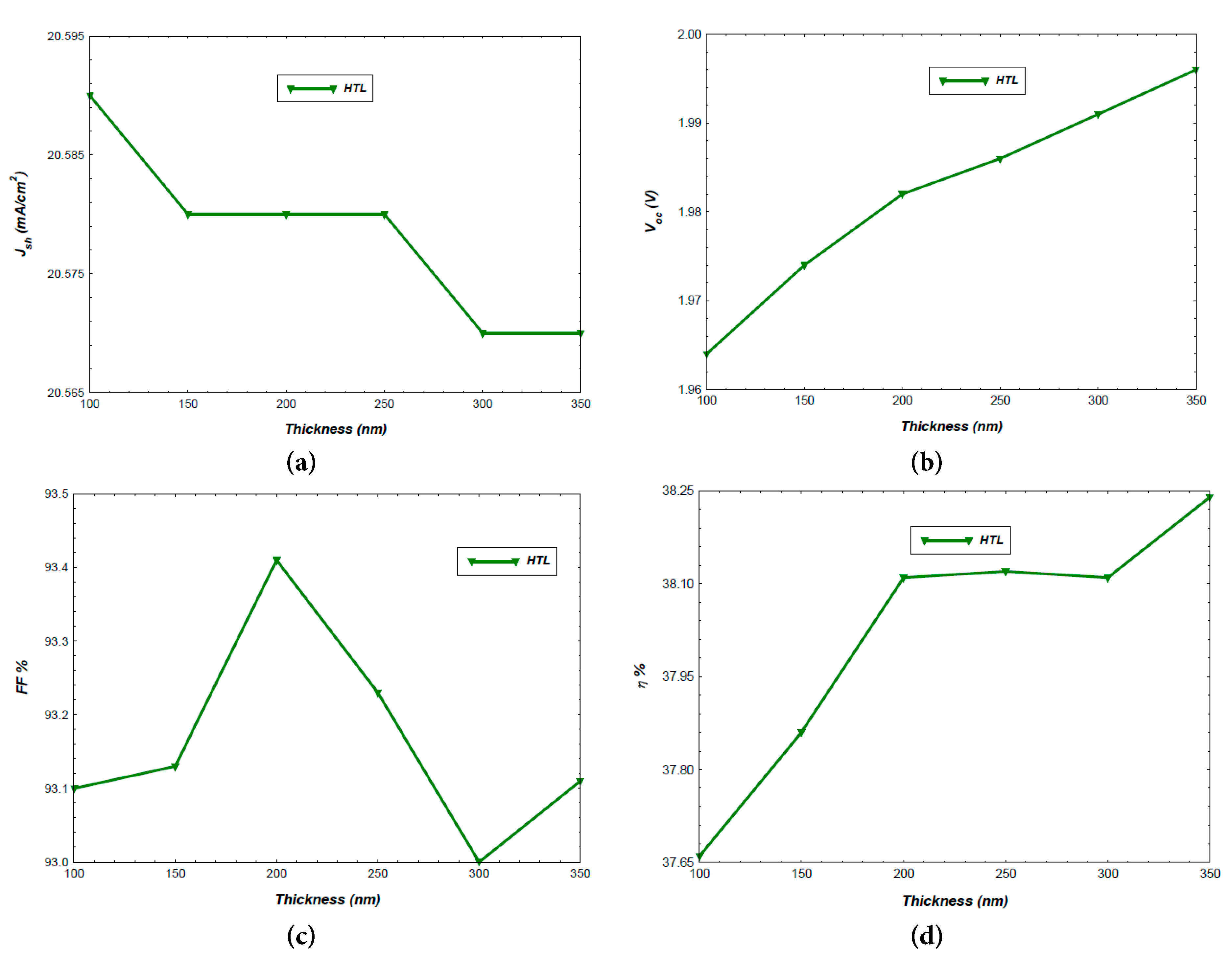
Figure 3: The obtained solar cell performance versus the ZnTe-HTL thickness: (a) Jsc, (b) Voc, (c) FF, and (d) η.
The (Jsc) remained essentially constant at 20.57–20.59 mA/cm2 throughout the thickness range, as observed in Fig. 3a, implying that optical absorption and carrier generation are unaffected by ZnTe thickness in this configuration. Fig. 3b shows that (Voc) a gradual increase with ZnTe thickness, rising from 1.964 V at 100 nm to 1.996 V at 350 nm. This indicates that a thicker ZnTe layer improves the built-in potential, possibly due to reduced interface recombination. This behavior provides important insights into the optical and electrical design of the optimized device architecture.
ZnTe has a bandgap of ~2.26 eV, which renders it transparent to photons with energy below this value—i.e., wavelengths longer than ~550 nm. However, in the present solar stack, all above-bandgap photons are already absorbed within the two perovskite absorber layers:
- The wide-gap top cell (CH3NH3PbI3−xClx, Eg ≈ 1.55 eV) absorbs photons in the 300–780 nm range.
- The narrow-gap bottom cell (CH3NH3SnI3, Eg ≈ 1.3 eV) absorbs photons in the 780–1000 nm range.
Since ZnTe lies behind both absorbers (adjacent to the reflective Au back contact), and since it does not absorb significantly in the spectral region where the bottom cell operates, increasing its thickness introduces negligible parasitic absorption. Consequently, the photogenerated carrier density remains unchanged, and Jsc stays constant.
The p++ZnTe layer is heavily doped (NA > 1019 cm−3), resulting in: high hole conductivity, short Debye length, and strong built-in field at the perovskite/ZnTe interface.
The insensitivity of Jsc to ZnTe thickness indicates that:
- The device is optically optimized: all usable photons are harvested in the perovskite stack; no significant light reaches or is lost in the HTL.
- The device is electrically optimized: the HTL provides ohmic, low-resistance contact with no bottleneck for hole transport.
- Recombination losses at the perovskite/ZnTe interface are minimal, likely due to favorable band alignment and low trap density.
Jsc often decreases with HTL thickness due to low mobility and parasitic absorption. The robustness of Jsc here underscores the advantage of inorganic, heavily doped HTLs like p++ZnTe in high-performance tandem PSCs.
The constant Jsc confirms that the architecture achieves complete photon harvesting and lossless hole extraction, validating the choice of ZnTe as an ideal HTL for all perovskite tandem solar cells.
The (FF) exhibits slight fluctuations between 93.00% and 93.41%. The highest FF is observed at 200 nm thickness, suggesting an optimal balance between reduced series resistance and minimal recombination. In addition, the (η) increases from 37.66% at 100 nm to a maximum of 38.24% at 350 nm, as depicted in Fig. 3c,d. The enhancement is primarily attributed to the combined effects of increased Voc and marginal improvements in FF, while Jsc remained stable.
4.3 Comparison of ETL and HTL Thickness Effects on Device Performance
When comparing the two layers, ZnO-ETL thickness variation had minimal impact on performance, while ZnTe-HTL thickness variation produced measurable improvements in Voc and η. The ETL performance plateau suggests that a thickness of 600 nm is adequate for optimal operation. The HTL, on the other hand, benefits from moderate thickening of 350 nm, which improves device efficiency without introducing significant resistive losses. This highlights the importance of targeted thickness optimization based on layer function within the device architecture. Comparison of the effects of ZnO-ETL and ZnTe-HTL thickness on photovoltaic performance parameters Voc, Jsc, FF, and η for the simulated double-heterojunction PSC with fixed absorber thicknesses of 800 nm for CH3NH3PbI3−xClx and CH3NH3SnI3 is determined in Fig. 4.
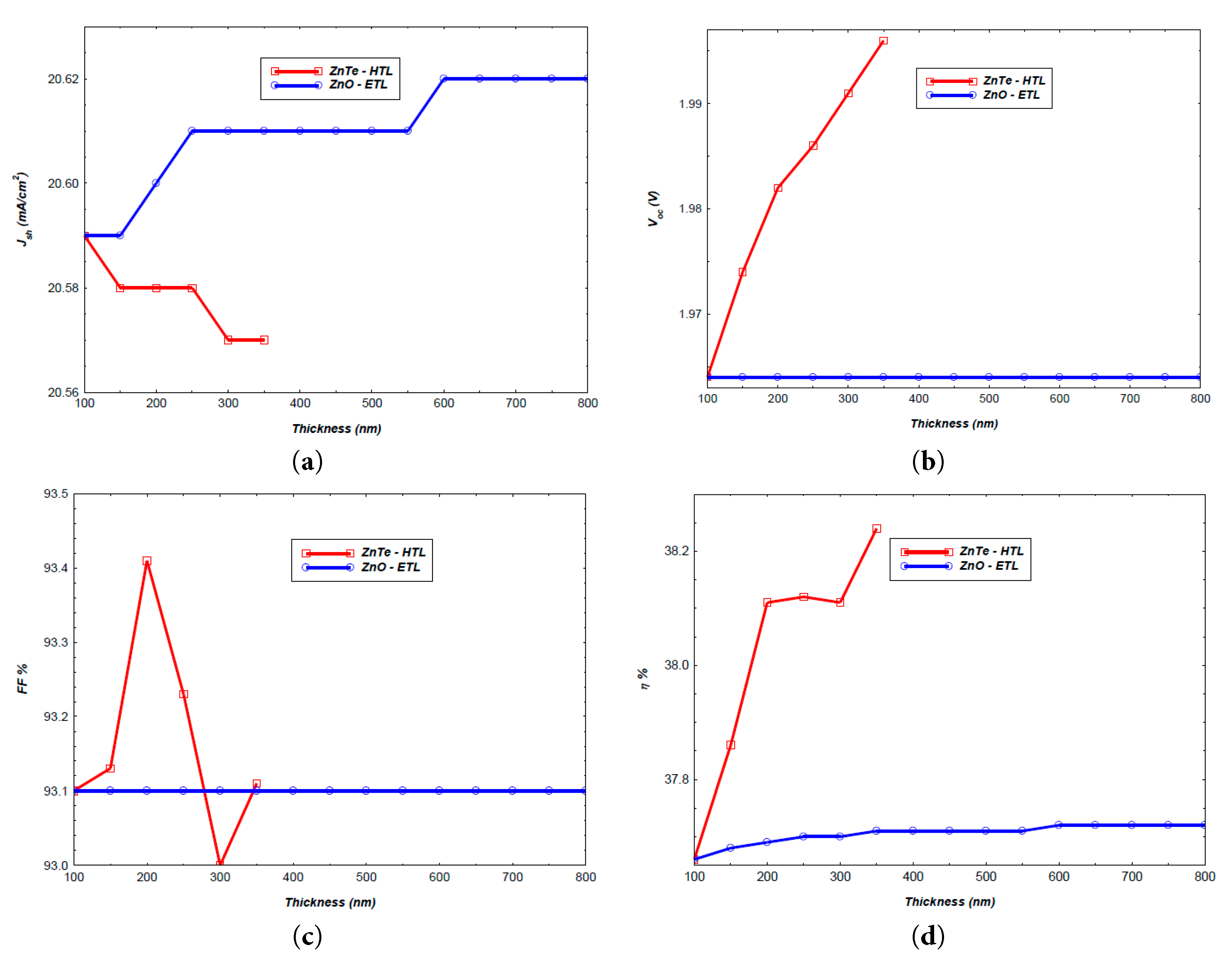
Figure 4: Comparison of the effects of ZnO-ETL and ZnTe-HTL thickness on photovoltaic PSC performance: (a) Jsc, (b) Voc, (c) FF, and (d) η.
4.4 Performance of the Optimized Device Configuration
The finalized device configuration consisted of an FTO layer (200 nm), ZnO-ETL (600 nm), CH3NH3PbI3−xClx and CH3NH3SnI3 absorber layers (800 nm each), and a ZnTe-HTL (350 nm). Simulation outputs include the J-V characteristics, quantum efficiency (QE) spectrum, Electric field distribution, and energy band diagram for this configuration, as shown in Fig. 5.
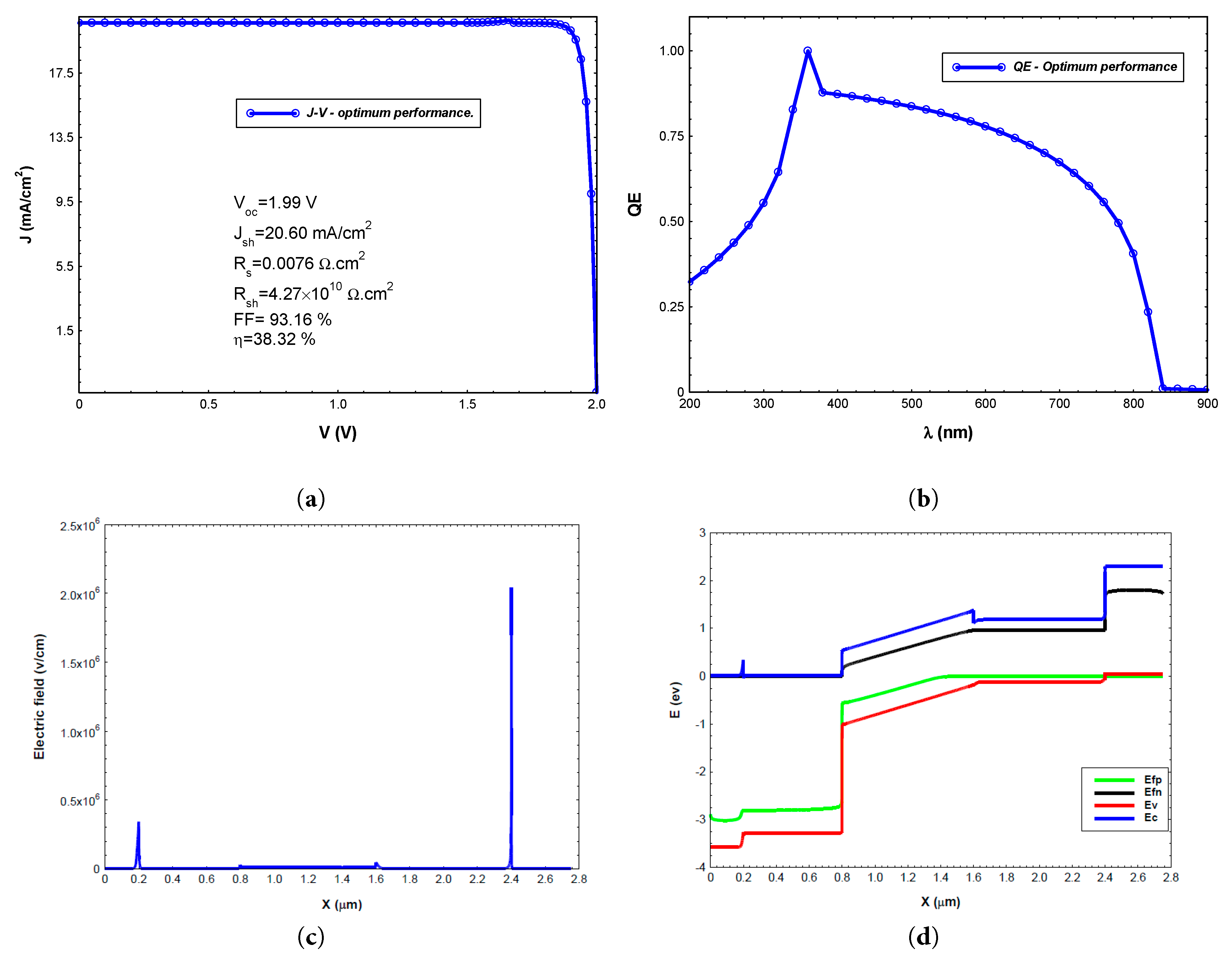
Figure 5: Simulated characteristics of the optimized double heterojunction solar cell: (a) J-V curve, (b) quantum efficiency spectrum, (c) electric field distribution, and (d) energy band diagram.
The simulated J-V curve for the optimized structure, Fig. 5a, shows an ideality factor of 0.999, a series resistance of 0.0076 Ω·cm2, a Jsc of approximately 20.60 mA/cm2, and a Voc of 1.996 V. The FF remains above 93%, leading to a power conversion efficiency of about 38.32%. The near-rectangular J-V curve shape indicates minimal resistive losses. More importantly, it confirms efficient carrier extraction, a key factor in the device’s high performance.
Fig. 5b demonstrates the QE spectrum with a strong photoresponse across a broad spectral range. Quantum efficiency begins at 32% at 200 nm, increases steadily with wavelength, and reaches a maximum exceeding 99% at 360 nm. It then averages around 80% in the visible range, from 400 to 700 nm. The QE drops sharply beyond about 780 nm, corresponding to the bandgap limitations of the absorber layers. The high, flat QE plateau across most of the visible spectrum confirms efficient photon absorption and carrier collection in both absorber layers.
The distribution of the simulated electric field (E) across the optimized solar cell’s thickness is shown in Fig. 5c. A sharp spike in E of 3.4 × 10⁵ V·cm−1 occurs at the transparent contact/ETL interface, creating the initial built-in field and facilitating electron collection into the ETL. A second, distinct maximum of 3 × 10⁴ V·cm−1 indicates the main electron-selective junction, where the field quickly dissociates photocarriers generated near the front absorber. A moderate peak of 5 × 10⁴ V·cm−1 appears at the internal absorber/absorber junction, aiding the movement of carriers across the band-gap step and reducing interfacial recombination between the two photoactive sub-layers. The most significant field enhancement, reaching about 2 × 10⁶ V·cm−1 at the hole-selective junction, ensures efficient hole extraction and effective electron blocking. Between these peaks, the field levels off to a nearly uniform plateau of 104 V·cm−1, sufficient to support drift-assisted transport across the absorber layers while minimizing resistive losses.
Fig. 5d displays the energy band diagram of the optimized double heterojunction solar cell. The conduction band edge (Ec), valence band edge (Ev), and the quasi-Fermi levels for electrons (Efn) and holes (Efp) are plotted across the whole device thickness (0–2.75 μm).
In the TCO region, Ec remains nearly flat at 0.02 eV, and Ev is positioned around −3.58 eV, confirming the wide bandgap and low recombination probability in this layer. At the TCO/ETL interface 0.20 μm, a sharp step in both Ec and Ev is observed, producing the internal potential barrier that drives carrier separation. Within the perovskite absorber region, Ec gradually rises from 0.3 eV to over 1.2 eV, while Ev shifts upward from −3.3 eV to −0.2 eV, showing strong band bending associated with photogenerated charge separation. Toward the HTL, the conduction band increases steeply to 2.3 eV, while the valence band aligns near −0.12 eV, which is favorable for hole transport and electron blocking.
The quasi-Fermi levels split substantially across both absorber sub-cells. The maximum Efn − Efp separation approaches about 2.0 eV, consistent with the measured Voc of 1.99 V at open circuit. The flat Efn near the ETL and the close tracking of Efp with the HTL valence band reflect efficient, selective contacts at both sides.
Table 2 compares the photovoltaic performance parameters of the optimized device with representative perovskite solar cells reported in the literature.
A numerical simulation study has successfully designed a double-heterojunction perovskite solar cell, FTO/ZnO/CH3NH3PbI3−xClx/CH3NH3SnI3/p++ZnTe/Au, which was performed. Through systematic parametric analysis using wxAMPS simulation software, the transport layers thicknesses were optimized for maximum performance. The results revealed that while ZnO (ETL) thickness variation from 100–800 nm had minimal influence on Voc, Jsc, FF, and η. While ZnTe (HTL) thickness played a more significant role, with moderate thickening up to ~350 nm enhancing Voc and overall efficiency. The optimized design achieved an efficiency of 38.32%, characterized by high voltage, stable current density, and a broad, high-plateau quantum efficiency spectrum. These outcomes high-light that, in multi-absorber-layer architectures, careful optimization of the hole-transport layer thickness is critical to performance gains. In contrast, electron transport layers can be kept thin to reduce processing costs without sacrificing efficiency. The study provides a clear design guideline for fabricating high-efficiency double-heterojunction PSCs, bridging the gap between simulation insights and experimental realization.
Acknowledgement:
Funding Statement: The author received no specific funding for this study.
Availability of Data and Materials: The data supporting the findings of this study are available from the corresponding author upon reasonable request. No publicly archived datasets were generated during the current study.
Ethics Approval: Not applicable.
Conflicts of Interest: The author declares no conflicts of interest.
References
1. Snaith HJ . Perovskites: The emergence of a new era for low-cost, high-efficiency solar cells. J Phys Chem Lett. 2013; 4( 21): 3623– 30. doi:10.1021/jz4020162. [Google Scholar] [CrossRef]
2. Green MA , Emery K , Hishikawa Y , Warta W . Solar cell efficiency tables (Version 31). Prog Photovolt. 2008; 16( 1): 61– 7. doi:10.1002/pip.808. [Google Scholar] [CrossRef]
3. Park NG . Perovskite solar cells: An emerging photovoltaic technology. Mater Today. 2015; 18( 2): 65– 72. doi:10.1016/j.mattod.2014.07.007. [Google Scholar] [CrossRef]
4. Kojima A , Teshima K , Shirai Y , Miyasaka T . Organometal halide perovskites as visible-light sensitizers for photovoltaic cells. J Am Chem Soc. 2009; 131( 17): 6050– 1. doi:10.1021/ja809598r. [Google Scholar] [CrossRef]
5. Afroz M , Ratnesh RK , Srivastava S , Singh J . Perovskite solar cells: Progress, challenges, and future avenues to clean energy. Solar Energy. 2025; 287: 113205. doi:10.1016/j.solener.2024.113205. [Google Scholar] [CrossRef]
6. Wang R , Mujahid M , Duan Y , Wang ZK , Xue J , Yang Y . A review of perovskites solar cell stability. Adv Funct Mater. 2019; 29( 47): 1808843. doi:10.1002/adfm.201808843. [Google Scholar] [CrossRef]
7. Schileo G , Grancini G . Lead or no lead? Availability, toxicity, sustainability and environmental impact of lead-free perovskite solar cells. J Mater Chem C. 2021; 9( 1): 67– 76. doi:10.1039/d0tc04552g. [Google Scholar] [CrossRef]
8. Zhang YY , Chen S , Xu P , Xiang H , Gong XG , Walsh A , et al. Intrinsic instability of the hybrid halide perovskite semiconductor CH3NH3PbI3. Chin Phys Lett. 2018; 35( 3): 036104. doi:10.1088/0256-307x/35/3/036104. [Google Scholar] [CrossRef]
9. Al-Ashouri A , Köhnen E , Li B , Magomedov A , Hempel H , Caprioglio P , et al. Monolithic perovskite/silicon tandem solar cell with >29% efficiency by enhanced hole extraction. Science. 2020; 370: 1300– 9. doi:10.1126/science.abd4016. [Google Scholar] [CrossRef]
10. Sahli F , Werner J , Kamino BA , Bräuninger M , Monnard R , Paviet-Salomon B , et al. Fully textured monolithic perovskite/silicon tandem solar cells with 25.2% power conversion efficiency. Nat Mater. 2018; 17( 9): 820– 6. doi:10.1038/s41563-018-0115-4. [Google Scholar] [CrossRef]
11. Xuan J , Shao T , Zang Y , Liu Y , Yan W . Recent developments of charge transporting layers for high-performance monolithic perovskite/silicon tandem solar cells. IEEE J Photovolt. 2025; 15( 1): 3– 16. doi:10.1109/JPHOTOV.2024.3483266. [Google Scholar] [CrossRef]
12. Park HH . Inorganic materials by atomic layer deposition for perovskite solar cells. Nanomaterials. 2021; 11( 1): 88. doi:10.3390/nano11010088. [Google Scholar] [CrossRef]
13. Wang Y , He J , Yang Y , Zhang Z , Long R . Chlorine passivation of grain boundary suppresses electron–hole recombination in CsPbBr3 perovskite by nonadiabatic molecular dynamics simulation. ACS Appl Energy Mater. 2019; 2( 5): 3419– 26. doi:10.1021/acsaem.9b00220. [Google Scholar] [CrossRef]
14. Wang X , Wang L , Shan T , Leng S , Zhong H , Bao Q , et al. Low-temperature aging provides 22% efficient bromine-free and passivation layer-free planar perovskite solar cells. Nano Micro Lett. 2020; 12( 1): 84. doi:10.1007/s40820-020-00418-0. [Google Scholar] [CrossRef]
15. Alla M , Manjunath V , Chawki N , Singh D , Yadav SC , Rouchdi M , et al. Optimized CH3NH3PbI3-XClX based perovskite solar cell with theoretical efficiency exceeding 30%. Opt Mater. 2022; 124: 112044. doi:10.1016/j.optmat.2022.112044. [Google Scholar] [CrossRef]
16. Chen Q , Zhou H , Hong Z , Luo S , Duan HS , Wang HH , et al. Planar heterojunction perovskite solar cells via vapor-assisted solution process. J Am Chem Soc. 2014; 136( 2): 622– 5. doi:10.1021/ja411509g. [Google Scholar] [CrossRef]
17. Chen W , Wu Y , Yue Y , Liu J , Zhang W , Yang X , et al. Efficient and stable large-area perovskite solar cells with inorganic charge extraction layers. Science. 2015; 350( 6263): 944– 8. doi:10.1126/science.aad1015. [Google Scholar] [CrossRef]
18. Hao F , Stoumpos CC , Cao DH , Chang RPH , Kanatzidis MG . Lead-free solid-state organic–inorganic halide perovskite solar cells. Nat Photonics. 2014; 8( 6): 489– 94. doi:10.1038/nphoton.2014.82. [Google Scholar] [CrossRef]
19. Noel NK , Stranks SD , Abate A , Wehrenfennig C , Guarnera S , Haghighirad AA , et al. Lead-free organic–inorganic tin halide perovskites for photovoltaic applications. Energy Environ Sci. 2014; 7( 9): 3061– 8. doi:10.1039/C4EE01076K. [Google Scholar] [CrossRef]
20. Sabba D , Mulmudi HK , Prabhakar RR , Krishnamoorthy T , Baikie T , Boix PP , et al. Impact of anionic Br–substitution on open circuit voltage in lead free perovskite (CsSnI3−xBrx) solar cells. J Phys Chem C. 2015; 119( 4): 1763– 7. doi:10.1021/jp5126624. [Google Scholar] [CrossRef]
21. Bagade SS , Patel PK . Salutary impact of spontaneous oxidation in CH3NH3SnI3 on CZTS-based solar cell. Sci Rep. 2025; 15( 1): 3056. doi:10.1038/s41598-024-74964-7. [Google Scholar] [CrossRef]
22. Patel PK . Device simulation of highly efficient eco-friendly CH3NH3SnI3 perovskite solar cell. Sci Rep. 2021; 11( 1): 3082. doi:10.1038/s41598-021-82817-w. [Google Scholar] [CrossRef]
23. Yu BB , Liao M , Zhu Y , Zhang X , Du Z , Jin Z , et al. Oriented crystallization of mixed-cation tin halides for highly efficient and stable lead-free perovskite solar cells. Adv Funct Mater. 2020; 30( 24): 2002230. doi:10.1002/adfm.202002230. [Google Scholar] [CrossRef]
24. Yuan X , Zhang Z , Wang M , He D , Lu Y , Hong F , et al. Dual-absorption-layer Heterojunction Strategy for enhancing the photovoltaic performance of all-perovskite tandem solar cell. Acta Phys Sin. 2025; 74( 14): 148802. doi:10.7498/aps.74.20250372. [Google Scholar] [CrossRef]
25. Liu Y , Heinzel D , Rockett A . A new solar cell simulator: WxAMPS. In: Proceedings of the 2011 37th IEEE Photovoltaic Specialists Conference; 2011 Jun 19–24; Seattle, WA, USA. doi:10.1109/pvsc.2011.6186517. [Google Scholar] [CrossRef]
26. Fonash SJ . Solar cell device physics. 2nd ed. Cambridge, MA, USA: Academic Press; 2010. [Google Scholar]
27. Salgado-Conrado L , Álvarez-Macías C , Reyes-Durán B . A review of simulation tools for thin-film solar cells. Materials. 2024; 17( 21): 5213. doi:10.3390/ma17215213. [Google Scholar] [CrossRef]
28. Nowsherwan GA . Performance engineering of Cs2InSbCl6 lead-free double perovskite solar cells: insights from DFT, SCAPS-1D, wxAMPS, AFORS-HET, Oghmanano, and COMSOL. Discov Mater. 2026; 6: 15. doi:10.1007/s43939-025-00466-6. [Google Scholar] [CrossRef]
29. Isoe W , Mageto M , Maghanga C , Mwamburi M , Odari V , Awino C . Thickness dependence of window layer on CH3NH3PbI3−xClx perovskite solar cell. Int J Photoenergy. 2020; 2020: 8877744. doi:10.1155/2020/8877744. [Google Scholar] [CrossRef]
30. Rana MS , Razzak MA . Optimization of a CH3NH3SnI3 based lead-free organic perovskite solar cell using SCAPS-1D simulator. Bull Electr Eng Inform. 2024; 13( 4): 2242– 50. doi:10.11591/eei.v13i4.7333. [Google Scholar] [CrossRef]
31. Nahid MN , Shah MS , Mamur H , Hosen R , Bhuiyan MRA . Optimizing lead-free CH3NH3SnI3 perovskite solar cells by using SCAPS-1D software. Chem Inorg Mater. 2024; 4: 100069. doi:10.1016/j.cinorg.2024.100069. [Google Scholar] [CrossRef]
32. Zyoud SH , Zyoud AH , Abdelkader A , Ahmed NM . Numerical simulation for optimization of ZnTe-based thin-film heterojunction solar cells with different metal chalcogenide buffer layers replacements: SCAPS-1D simulation program. Int Rev Model Simul IREMOS. 2021; 14( 2): 79. doi:10.15866/iremos.v14i2.19954. [Google Scholar] [CrossRef]
33. Isah M , Doroody C , Rahman KS , Harif MN , Tiong SK , Amin N . A numerical analysis of ZnTe/AZO as tunnel junction in CdTe/Si tandem solar cell. IOP Conf Ser Mater Sci Eng. 2023; 1278( 1): 012003. doi:10.1088/1757-899X/1278/1/012003. [Google Scholar] [CrossRef]
34. Çetinkaya S . Study of electrical effect of transition-metal dichalcogenide-MoS2 layer on the performance characteristic of Cu2ZnSnS4 based solar cells using wxAMPS. Optik. 2019; 181: 627– 38. doi:10.1016/j.ijleo.2018.12.122. [Google Scholar] [CrossRef]
35. Chen W , Huang X , Cheng Q , Chen C , Yun D , Zhang F . Simulation analysis of heterojunction ZnO/CdS/Cu(In,Ga)Se2 thin-film solar cells using wxAMPS. Optik. 2016; 127( 1): 182– 7. doi:10.1016/j.ijleo.2015.09.198. [Google Scholar] [CrossRef]
36. Li C , Zhou J , Song J , Xu J , Zhang H , Zhang X , et al. Non-fullerene acceptors with branched side chains and improved molecular packing to exceed 18% efficiency in organic solar cells. Nat Energy. 2021; 6( 6): 605– 13. doi:10.1038/s41560-021-00820-x. [Google Scholar] [CrossRef]
37. Tahir S , Mushtaq S , McQueen J , Iqbal J , Almufarij RS , Alqurashi RS , et al. Computational insights into wide bandgap lead free perovskite solar cells for silicon based tandem configurations. Sci Rep. 2025; 15( 1): 20020. doi:10.1038/s41598-025-04637-6. [Google Scholar] [CrossRef]
Cite This Article
 Copyright © 2026 The Author(s). Published by Tech Science Press.
This work is licensed under a Creative Commons Attribution 4.0 International License , which permits unrestricted use, distribution, and reproduction in any medium, provided the original work is properly cited.
 Downloads
 Citation Tools