
 Submit a Paper
 Propose a Special lssue
 Open Access
ARTICLE

Performance Measurement of Energy Efficient and Highly Scalable Hybrid Adder
Anna University Regional Campus, Coimbatore, Tamilnadu, India
* Corresponding Author: B. Annapoorani. Email:
Computer Systems Science and Engineering 2023, 45(3), 2659-2672. https://doi.org/10.32604/csse.2023.025075
Received 10 November 2021; Accepted 15 February 2022; Issue published 21 December 2022
 View Full Text
 Download PDF
Abstract
The adders are the vital arithmetic operation for any arithmetic operations like multiplication, subtraction, and division. Binary number additions are performed by the digital circuit known as the adder. In VLSI (Very Large Scale Integration), the full adder is a basic component as it plays a major role in designing the integrated circuits applications. To minimize the power, various adder designs are implemented and each implemented designs undergo defined drawbacks. The designed adder requires high power when the driving capability is perfect and requires low power when the delay occurred is more. To overcome such issues and to obtain better performance, a novel parallel adder is proposed. The design of adder is initiated with 1 bit and has been extended up to 32 bits so as verify its scalability. This proposed novel parallel adder is attained from the carry look-ahead adder. The merits of this suggested adder are better speed, power consumption and delay, and the capability in driving. Thus designed adders are verified for different supply, delay, power, leakage and its performance is found to be superior to competitive Manchester Carry Chain Adder (MCCA), Carry Look Ahead Adder (CLAA), Carry Select Adder (CSLA), Carry Select Adder (CSA) and other adders.Keywords
VLSI applications comprises of digital signal processing, image and video processing, microprocessors and microcontrollers, which make extensive consumption of arithmetic operations. In several arithmetic operations, addition, subtraction, multiplication plus accumulation are generally utilized [1]. The most basic arithmetic operation is addition and several adders are utilized in VLSI. Key building block [2] of the Arithmetic and logic unit (ALU) is adder therefore, increasing its effect on speed and decreasing its power consumption will greatly disturb the speed yet power consumption of the processor. Several experiments have been under taken to optimize the speed and power of these units, obviously there is great need to accomplish higher speed at low power consumption, which is a task for designers.
Generally, the rise in speed is reached at the expense of more power consumption of the precision processing unit. Sacrificing the accuracy of the estimation is one of the strategies to enhance both power and speed. Researchers in the field of approximate calculation pay distinct consideration to adders. The hybrid adder is concentrated in [3], in which it is recommended to use the approximate Reverse Carry Propagation Full Adder (RCPFA), it transmits the input carry in a reverse flow, that is, to begin a carry output starting the higher substantial bit towards lower substantial bit. Due to reverse propagation, the carry weight decreases with the propagation, moreover the adder is less susceptible to delay changes and increase the delay of about 27%. The Lower part OR Adder (LOA) [4], splits the n-bit adder into two sub-adders where, the high significant sub-adder consists of
For the implementation of full adder circuits hybrid logic style is exploited. The design based on hybrid MTJ/CMOS (Magnetic tunnel junction/Complementary metal–oxide–semiconductor)can solve the leakage problem and bring the advantage of non-volatility using low power magnetic full-adder (MFA) [7]. MFA can withstand any particle impact, regardless of the induced charge, however radiation induced soft errors are still a problem in this adder. Many circuits with hybrid structure have been implemented, which are faster than the C-MOS and ingest less power and this presentation is used in several applications like portable and IOT (Internet Of Things) devices. It is predictable to use simple and effective timing behaviors like conventional logic effort to analyze hybrid adder circuit [8]. In accurate selection, the introduced standards are gain and selection factor and for the administration of energy efficiency and performance adjustment, hybrid adder cells are calculated over single test bench for the period of optimization. In relations of delay, power and driving capability hybrid FA’s [9] enactment is mostly hooked on the XOR-XNOR circuit enactment. Cadence virtuoso environs with 90-nm CMOS expertise is used for the recreation of this enactment. The driving capabilities are calculated by 2, 4, 8-bit cascaded full adder with inserted FA’s, it minimize the power delay up to 7.5%. For examining state-of the art approximate adders [10] designed on behalf of executing ASIC in add yet shift accelerators to practice the function of video and image. In the existence of frequent and low magnitude sum errors, then the description is done by the approximate adders. This adder provides main concern towards the power-efficiency, and results in the reduction of power about 7.7%. The adders output by means of fault is demonstrated by means of single stuck at fault, and its exists fought through the appraisal with projected similarity in sum using similarity of sum (i.e., sum bits are compared with the carry output) in multi-block carry select adder [11]. In this adder the appeared fault is spotted in advance the existence of next fault, the detection of error and easy testability functions are used to predict the fault all through the process. New full swing XOR-XNOR or XOR/XNOR gates [12] based hybrid 1-bit full adder [13] takes its scheduled qualities as speed, power consumption, power delay product, driving ability etc. This adder overcomes the disadvantages like critical path and positive feedback on output side.
Accuracy-configurable adder (ACA) [14] design is urbanized to accommodate dynamic level of calculation, and delay adaptive self-configurable performance is projected to develop accuracy delay transaction. Clamped-clamped micro beam resonator based on digital circuit execution through multiple split electrodes, where the resonant frequency is regulated by input logics in compact full adder [15]. Logic inputs resonant frequency is used to operate this adder, in which the input and output of the resonator are not well-matched. Computation in memory parallel adder [16], is used to analyze the feasibility in depth and it contains high scalability. Parallel addition is established by scheduled binary reduction tree yet lower bound time complication (
In this paper, we focus on the novel parallel adder that attained from the carry look-ahead adder. Carry look-ahead adder expands speed via minimizing the propagation time in determining carry, and extensively utilized in all electronic circuits and cannot fulfill the expected goal. To overcome this, a novel parallel adder is suggested to recognize efficient enactment. In this proposed system, simulation is prepared for 8-bit input data. The speed and power consumption and power speed products are measured for performance analysis.
2.1 Proposed XOR-XNOR Cell Scheme
In Fig. 1, the module 1 structure represents the XOR-XNOR cell that create a signal H and
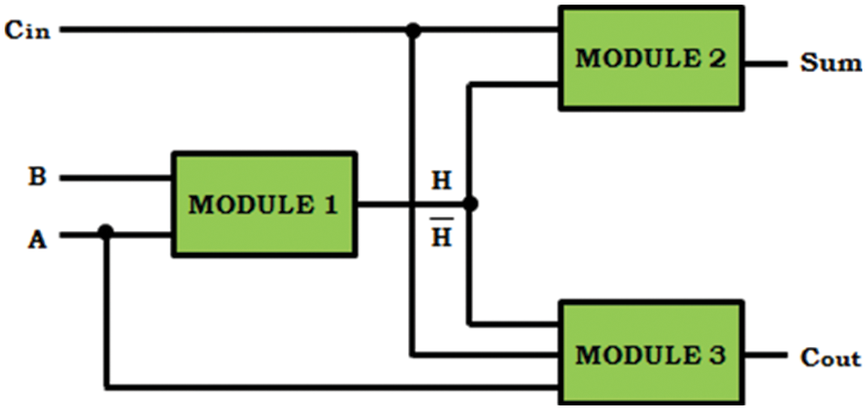
Figure 1: Hybrid design of full adder cells
The circuit at Fig. 2 represents the proposed XOR-XNOR cell where, both the outputs are created instantaneously. From the Fig. 2, the weak logic ‘0’
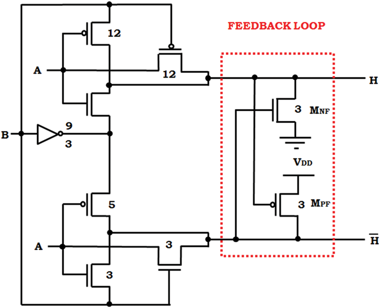
Figure 2: Proposed XOR-XNOR cell
The XOR-XNOR cell consists of 12 possible transitions (Initiated by the combination of input, AB = ‘00’ and it is varied to ‘01’, then again to ‘00’ now it is changed ‘00’ to ‘10’ and rapidly goes on, thus the formation of the 12 transitions are achieved). The time interval of the input to obtain the voltage supply of about 50% and the same level obtained by the output are calculated yet the obtained worst-case is recognized as the cell delay propagation. The average of the power dissipation is fixed from the consumption of average power in all illustrations are considered from the 12 transition inputs. The value of PDP is calculated as,
The module-2 of proposed hybrid full adder indicates XOR cell and is shown in Figs. 3a–3e. The conventional LP-XOR, 3 T-XOR, inverter-based XOR and P-XOR cells utilize a maximum of only four transistors but they fail to produce full swing output and hence they are not suitable for cascaded architectures. In the proposed XOR cell, a GDI based XOR cell which has four transistors and also provides full swing output is employed to implement module-2 setup.
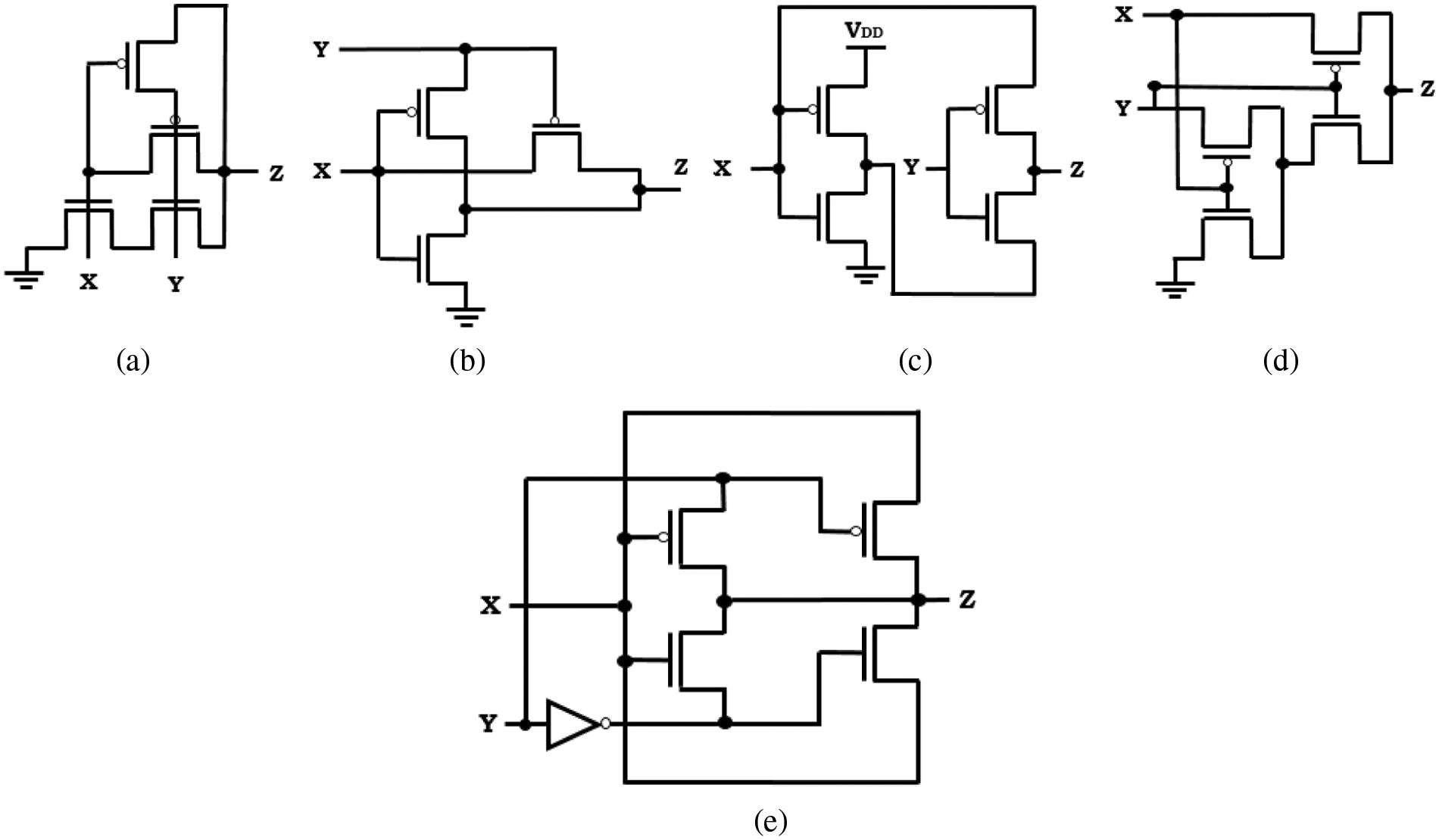
Figure 3: Module-2 circuit possibilities (a) LP-XOR circuit, (b) 3 T-XOR circuit, (c) inverter-based XOR circuits (d) P-XOR circuits
The 2-to-1 multiplexer also remains as hybrid full adder of third module as per the Fig. 1. Certain suggested 2-to-1 MUX circuits are characterized at Fig. 3, in which the input, select lines then outputs be signified as sel, x, y also z correspondingly.
Two pass transistor is used by 2-to-1 multiplexers in Figs. 4a–4c, however the generated output is an non-full swing this is the major dis-advantage. Improper concert is yielded by the entire circuits because of the occurrence of voltage degradation, this happens when the successive stages are connected by the degraded output. This declared tricky is eradicated through concerning two circuits of Fig. 3c composed with Fig. 3d, however the single pMOS and single nMOS transistors are conducted at the respective combination of input. At node z, logic ‘0’ is yielded by way of passing logic ‘0’ over Mn2 when the occurrence is set to sel = x = 0 else the logic ‘1’ is yielded by way of passing logic ‘1’ over Mp2 at the occurrence sel = y = 1. In the design of our full adder, at Fig. 3d, 2–1 MUX is nominated in place of module 3 to gratify the property full-swing.
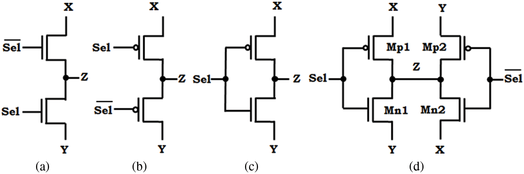
Figure 4: 2:1 Mux circuit topologies
2.3 Design of Proposed Full Adder Cell
The whole circuit of the suggested hybrid full adder is employed by Fig. 1 configuration is demonstrated in Fig. 4.
The full-swing property is assured and the outputs are created independently, in this suggested full adder, which is illustrated in Fig. 5. To achieve the target of small chip capacity, the 18 MOSFETs are used totally to design the circuit. The considered XOR-XNOR cell’s speed is utilized as Module 1 by the suggested full adder circuit is satisfactory. Only two-pass transistor is used to perform the input carry to output carry propagation in our proposed design, hence reduce of the RCA’s cascaded structure’s speed is affected by the delay in propagation of carry this is an advantage of our design.
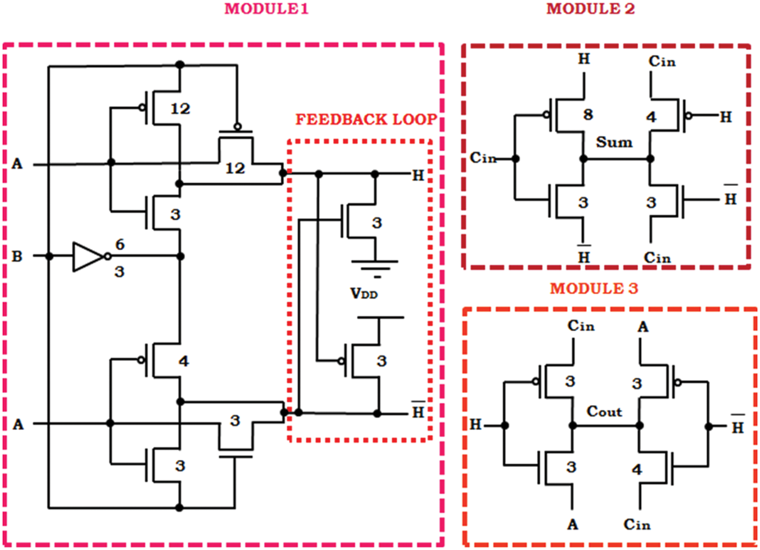
Figure 5: Transistor level proposed full adder
Static and dynamic are the two major constituents of CMOS in the consumption of power (switching and short-circuit are the other two contributes of dynamic power), it is represented as,
Clock frequency, voltage swing at node i, capacitance load at node i, activity factor at node i are represented as
The operation of the proposed full adder shown in Fig. 6 is exhibited in the simulation environment. To provide a realistic environment, the buffers are used at the input and output of the cell. The maximum number of transistor used in this proposed adder is 16 with 1.8 V supply voltage and 100 MHz frequency in 180 nm technology. At the output of adder cell, an inverter is connected in series with the load capacitance. The size of buffer and inverter are restricted by signal degradation and fan-out. The entire work is validated in xilinx ISE Desigh Suite 13.4 software.
Figure 6: Simulation setup
The layout of proposed 1-bit full adder shown in Fig. 6 is drawn in cadence tool using two lines as per the design procedure. The ultimate aim of designing any VLSI adder is to minimize the circuit area, time delay and power however it is difficult to reduce all factor simultaneously. Hence for effective comparison, the tradeoffs among the factors are needed to be considered. The overall performance of the adder is accessed by measuring the values of FOM. The FOM is expressed as
The full adder performance in contrast to the input noise is assessed by eliminating the input buffers and the input cells are linked straightly towards the full adder cells. The scalability in our proposed adder is best when compared with other adders. The presentation of the suggested full adder is examined in contrast with environmental conditions and variations in manufacturing and this performance are represented in the Fig. 7.
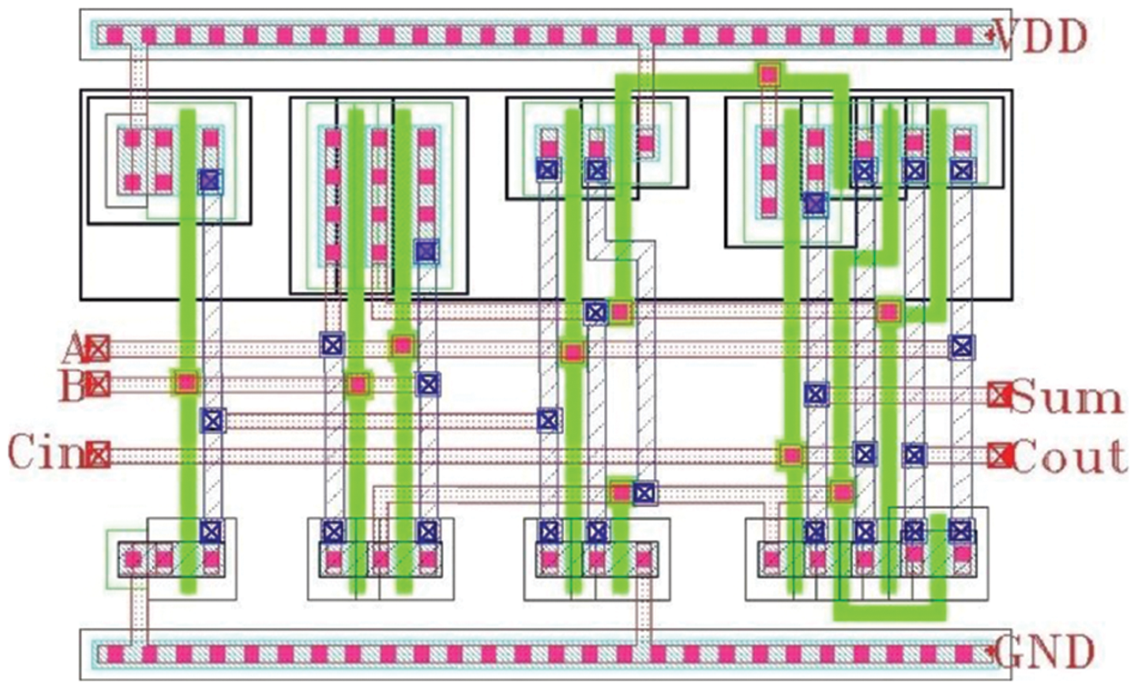
Figure 7: Layout of proposed 1-bit
The full adder circuit is designed to moderate the consumption of power values, area and delay these are the major resolution of this adder. Thus these improvements are done by our proposed novel parallel adder. To prove the performance of the proposed adder the comparison is made between several set of adders, which is portrayed in Figs. 8–11. And the comparative analysis of different 1-bit adders is provided as shown in Tab. 1.
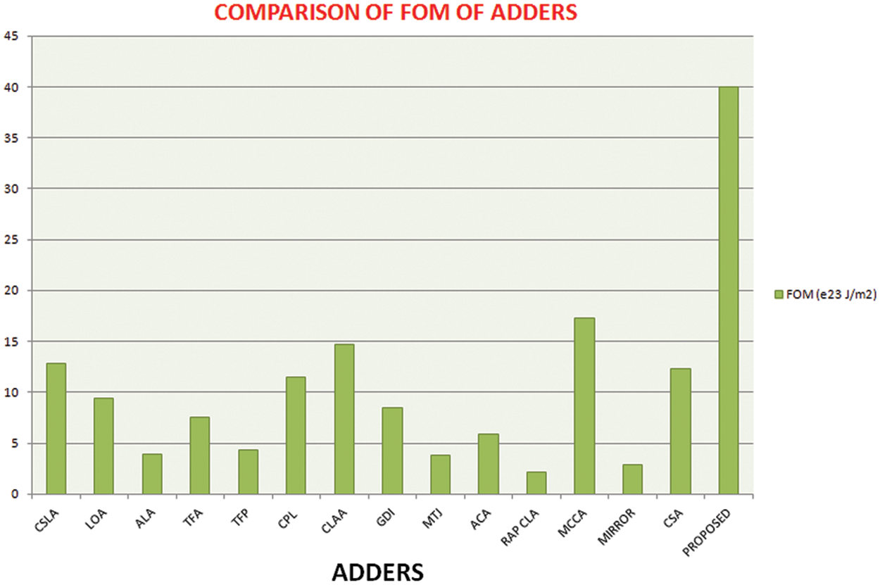
Figure 8: Comparison of FOM of various adders
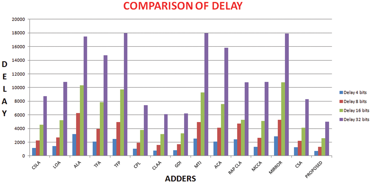
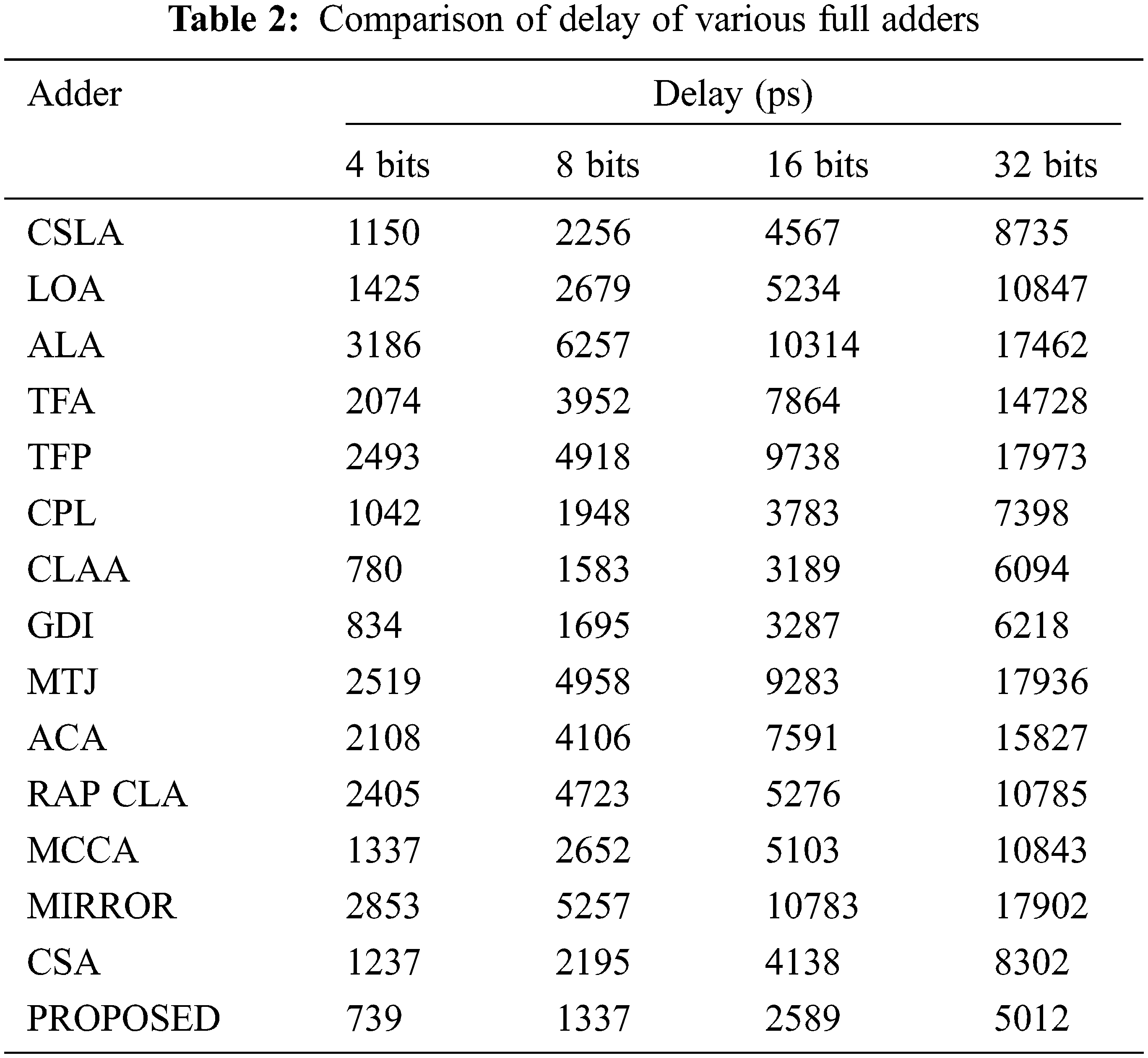
Figure 9: Comparison of delay of 4-bits, 8-bits, 16-bits and 32bits adders
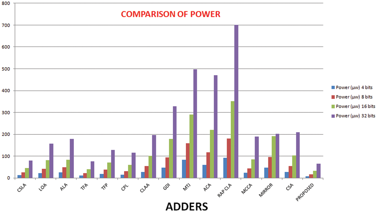
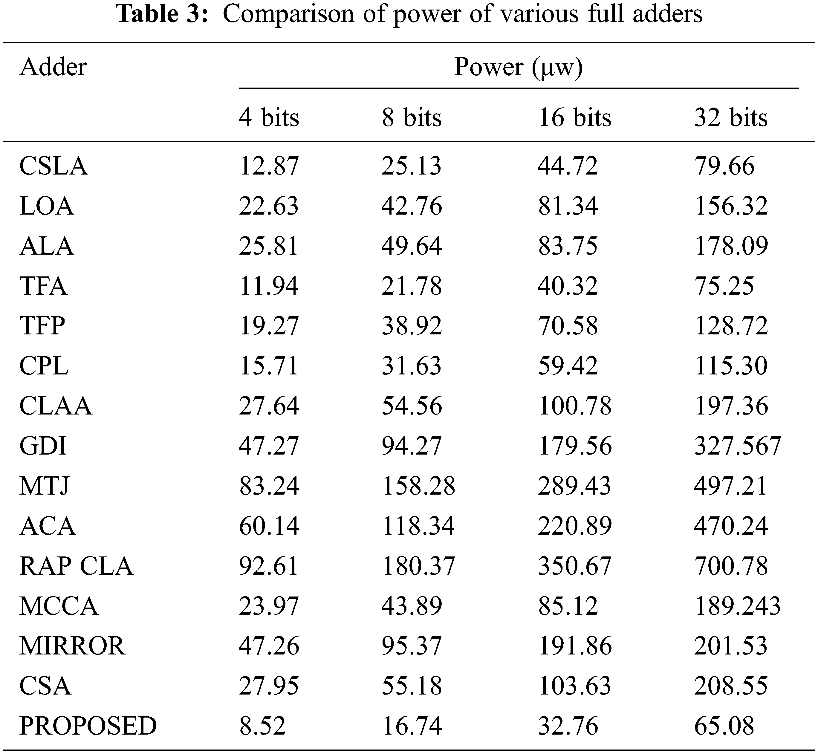
Figure 10: Comparison of power of 4-bits, 8-bits, 16-bits and 32bits adders
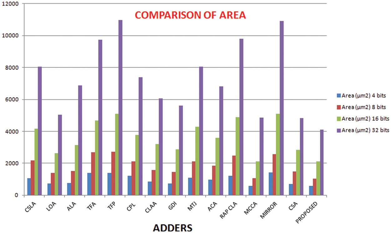
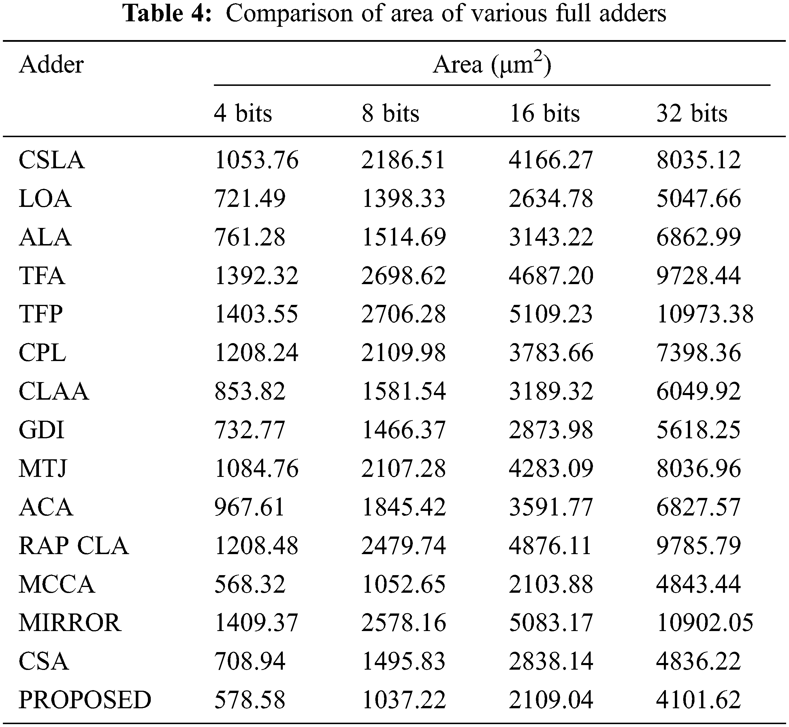
Figure 11: Comparison of area of 4-bits, 8-bits, 16-bits and 32bits adders
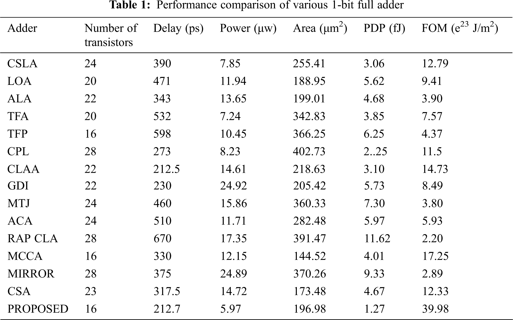
To get optimized performance from the proposed adder, the power, delay and its product are minimized by reducing the transistors sizes. In an ideal environment, several existing competitive adders are considered to compare with the proposed 1-bit adder. The CPL and RAP CLA adder require 28 transistors whereas the proposed cell requires only 16 transistors. Even though, the MCCA cell has less number of transistors, the delay (330 ps) is comparatively higher the proposed cell. Among the available adders, the power consumption of MIRROR and GDJ are very high while the CSLA, ALA and the proposed cell require less power.
It is necessary to improve the performance of designed 1-bit adder cell so that it will perform well when deployed in real time environment. This is significantly important for cascaded connected adders where the drivers may not give sufficiently strengthened input signal to the cells. The total mortification in signal level may prompt defective yield and the circuit may glitch under low voltages.
The inputs of the adder cells are fed via the buffers to include the consequences of input capacitances and the outputs are also stacked with buffers to ensure proper loadings. The full adder is also experimented in simulation setup. These test benches have three similar buffer prototypes at the input and two at the output. The only difference is the number of adder stages used in between the input and output as well as the number of stages increases gradually depending on number of bits involved. It is noticed that the propagation delay starts to rise significantly in the order of two. The performance parameters (delay, power and area) are measured individually for 4 bits, 8 bits 16 bits and 32 bits as shown in Tabs. 2, 3 and 4. Numerous arbitrary test patterns were given at the inputs and the simulation results of the adder cells were used for comparison. The performance analysis of the proposed full adder was performed with variation in number of bits for 180 nm technology.
While testing, the design with the fewer input, the proposed adder plays a better performance and for some input patterns it stuck with errors. These patterns are delivered as the input towards the design yet the output is noted at the condition for which each required output is corresponding to the each input, thereby the design is set free from the errors. The error stuck that present in the design after manufacturing is found by utilizing these patterns. The input test patterns that essential to investigate a number of adder’s 8-bit, 16-bit, 32-bit and 64-bit are shown at the Fig. 7.
In this paper, the markedly improved novel hybrid adder is presented and implemented with different logic styles. The attributes of proposed adder are compared with various digital adders to prove the effectiveness of proposed scheme. Initially XOR-XNOR cell is modeled then with the help of this cell, a novel parallel adder is designed by incorporating additional modules. When extended for higher bits, the strength of this adder is improved by eliminating the buffers at the input and output ports. This proposed adder is then compared with various adders that are proposed in the previous and obtain the power consumption of about 18% when compared to other adders it is less. The proposed novel parallel adder is designed to dissipate low power, consume less area and operate at high speed. From the comprehensive comparative analysis, it is clear that a high scalability and FOM was delivered by the designed adder cell even when the bit length has been extended up to 32bits. Further the performance of proposed adder with cascaded configuration is to discussed in future.
Funding Statement: The authors received no specific funding for this study.
Conflicts of Interest: The authors declare that they have no conflicts of interest to report regarding the present study.
References
1. M. Bahadori, M. Kamal, A. A. Kusha and M. Pedram, “High-speed and energy-efficient carry skip adder operating under a wide range of supply voltage levels,” IEEE Transactions on Very Large Scale Integration (VLSI) Systems, vol. 24, no. 2, pp. 421–433, 2015. [Google Scholar]
2. A. Dalloo, A. Najafi and A. G. Ortiz, “Systematic design of an approximate adder: The optimized lower part constant-OR adder,” IEEE Transactions on Very Large Scale Integration (VLSI) Systems, vol. 26, pp. 1595–1599, 2018. [Google Scholar]
3. M. Pashaeifar, M. Kamal, A. A. Kusha and M. Pedram, “Approximate reverse carry propagate adder for energy-efficient DSP applications,” IEEE Transactions on Very Large Scale Integration (VLSI) Systems, vol. 26, no. 11, pp. 2530–2541, 2018. [Google Scholar]
4. Y. S. Mehrabani and M. Eshghi, “Noise and process variation tolerant, low-power, high-speed, and low-energy full adders in CNFET technology,” IEEE Transactions on Very Large Scale Integration (VLSI) Systems, vol. 24, no. 11, pp. 3268–3281, 2016. [Google Scholar]
5. A. S. Roy, R. Biswas and A. S. Dhar, “On fast and exact computation of error metrics in approximate LSB adders,” IEEE Transactions on Very Large Scale Integration (VLSI) Systems, vol. 28, no. 4, pp. 876–889, 2020. [Google Scholar]
6. V. Pudi, K. Sridharan and F. Lombardi, “Majority logic formulations for parallel adder designs at reduced delay and circuit complexity,” IEEE Transactions on Computers, vol. 66, no. 10, pp. 1824–1830, 2017. [Google Scholar]
7. R. Rajaei and S. B. Mamaghani, “Ultra-low power, highly reliable, and nonvolatile hybrid MTJ/CMOS based full-adder for future VLSI design,” IEEE Transactions on Device and Materials Reliability, vol. 17, no. 1, pp. 213–220, 2017. [Google Scholar]
8. T. Nikoubin, “Hybrid logical effort for hybrid logic style full adders in multistage structures,” IEEE Transactions on Very Large Scale Integration (VLSI) Systems, vol. 27, no. 5, pp. 1138–1147, 2019. [Google Scholar]
9. C. L. Ayala, N. Takeuchi, Y. Yamanashi, T. Ortlepp and N. Yoshikawa, “Majority-logic-optimized parallel prefix carry look-ahead adder families using adiabatic quantum-flux-parametron logic,” IEEE Transactions on Applied Superconductivity, vol. 27, no. 4, pp. 1–7, 2021. [Google Scholar]
10. W. Liu, L. Chen, C. Wang, M. O. Neill and F. Lombardi, “Design and analysis of inexact floating-point adders,” IEEE Transactions on Computers, vol. 65, no. 1, pp. 308–314, 2015. [Google Scholar]
11. H. A. Du Nguyen, L. Xie, M. Taouil, R. Nane, S. Hamdioui et al., “On the implementation of computation-in-memory parallel adder,” IEEE Transactions on Very Large Scale Integration (VLSI) Systems, vol. 25, no. 8, pp. 2206–2219, 2017. [Google Scholar]
12. N. Kito and N. Takagi. “Concurrent error detectable carry select adder with easy testability,” IEEE Transactions on Computers, vol. 68, no. 7, pp. 1105–1110, 2019. [Google Scholar]
13. J. Kandpal, A. Tomar, M. Agarwal and K. K. Sharma, “High-speed hybrid-logic full adder using high-performance 10-T XOR–XNOR cell,” IEEE Transactions on Very Large Scale Integration (VLSI) Systems, vol. 28, no. 6, pp. 1413–1422, 2020. [Google Scholar]
14. S. K. Sahoo, G. Akhilesh, R. Sahoo and M. Muglikar, “High-performance ternary adder using CNTFET,” IEEE Transactions on Nanotechnology, vol. 16, no. 3, pp. 368–374, 2017. [Google Scholar]
15. L. B. Soares, M. M. A. da Rosa, C. M. Diniz, E. A. C. Da Costa and S. Bampi, “Design methodology to explore hybrid approximate adders for energy-efficient image and video processing accelerators,” IEEE Transactions on Circuits and Systems I: Regular Papers, vol. 66, no. 6, pp. 2137–2150, 2019. [Google Scholar]
16. H. Naseri and S. Timarchi, “Low-power and fast full adder by exploring new XOR and XNOR gates,” IEEE Transactions on Very Large Scale Integration (VLSI) Systems, vol. 26, no. 8, pp. 1481–1493, 2018. [Google Scholar]
17. S. G. Rohani, N. Taherinejad and D. Radakovits, “A semiparallel full-adder in IMPLY logic,” IEEE Transactions on Very Large Scale Integration (VLSI) Systems, vol. 28, no. 1, pp. 297–301, 2017. [Google Scholar]
18. W. Xu, S. S. Sapatnekar and J. Hu, “A simple yet efficient accuracy-configurable adder design,” IEEE Transactions on Very Large Scale Integration (VLSI) Systems, vol. 26, no. 6, pp. 1112–1125, 2018. [Google Scholar]
19. S. Ahmed, S. Ilyas, X. Zou, N. Jaber, M. I. Younis et al., “A compact adder and reprogrammable logic gate using micro-electromechanical resonators with partial electrodes,” IEEE Transactions on Circuits and Systems II: Express Briefs, vol. 66, no. 12, pp. 2057–2061, 2019. [Google Scholar]
20. T. Zhang, V. Pudi and W. Liu, “New majority gate-based parallel BCD adder designs for quantum-dot cellular automata,” IEEE Transactions on Circuits and Systems II: Express Briefs, vol. 66, no. 7, pp. 1232–1236, 2019. [Google Scholar]
21. O. Akbari, M. Kamal, A. A. Kusha and M. Pedram, “RAP-CLA: A reconfigurable approximate carry look-ahead adder,” IEEE Transactions on Circuits and Systems II: Express Briefs, vol. 65, no. 8, pp. 1089–1093, 2016. [Google Scholar]
22. F. E. Azandaryani, O. Akbari, M. Kamal, A. A. Kusha and M. Pedram, “Block-based carry speculative approximate adder for energy-efficient applications,” IEEE Transactions on Circuits and Systems II: Express Briefs, vol. 67, no. 1, pp. 137–141, 2019. [Google Scholar]
23. B. K. Mohanty, “Efficient fixed-width adder-tree design,” IEEE Transactions on Circuits and Systems II: Express Briefs, vol. 66, no. 2, pp. 292–296, 2018. [Google Scholar]
24. J. Villalba, J. Hormigo and S. G. Navarro, “Fast HUB floating-point adder for FPGA,” IEEE Transactions on Circuits and Systems II: Express Briefs, vol. 66, no. 6, pp. 1028–1032, 2019. [Google Scholar]
25. A. Nannarelli, “Tunable floating-point adder,” IEEE Transactions on Computers, vol. 68, no. 10, pp. 1553–1560, 2019. [Google Scholar]
Cite This Article
 Copyright © 2023 The Author(s). Published by Tech Science Press.
This work is licensed under a Creative Commons Attribution 4.0 International License , which permits unrestricted use, distribution, and reproduction in any medium, provided the original work is properly cited.
 Downloads
 Citation Tools