
 Submit a Paper
 Propose a Special lssue
 Open Access
ARTICLE

Semiconducting SWCNT Photo Detector for High Speed Switching Through Single Halo Doping
1 Department of Information and Communication Engineering, Anna University, Chennai, 600025, Tamilnadu, India
2 Department of Electronics and Communication Engineering, VeltechMultitech Dr. RR Dr. SR Engineering College, Chennai-42, Tamilnadu, India
* Corresponding Author: A. Arulmary. Email:
Computer Systems Science and Engineering 2023, 46(2), 1617-1630. https://doi.org/10.32604/csse.2023.034681
Received 24 July 2022; Accepted 03 November 2022; Issue published 09 February 2023
 View Full Text
 Download PDF
Abstract
The method opted for accuracy, and no existing studies are based on this method. A design and characteristic survey of a new small band gap semiconducting Single Wall Carbon Nano Tube (SWCNT) Field Effect Transistor as a photodetector is carried out. In the proposed device, better performance is achieved by increasing the diameter and introducing a new single halo (SH) doping in the channel length of the CNTFET device. This paper is a study and analysis of the performance of a Carbon Nano Tube Field Effect Transistor (CNTFET) as a photodetector using the self-consistent Poisson and Green function method. The 2D self-consistent Poisson and Green’s function method for various optical intensities and wavelength simulate this proposed photodetector. The performance study is based on the simulation of drain current, transconductance, sub-threshold swing, cut-off frequency, gain, directivity, and quantum efficiency under dark and illuminated conditions. These quantum simulation results show that cut-off frequency increases while there is an increase in diameter. The proposed SH-CNTFET provides better performance in terms of higher gain and directivity than conventional CNTFET (C-CNTFET). This device will be helpful in optoelectronic integrated circuits (OEIC) receivers due to its superior performance.Keywords
CNTFETs have been studied, and their characteristics have been analyzed in various forms. CNTFETs have been designed and fabricated with varying parameters, and evolution is still in the making. Significant studies related to the proposed model include the following. The Gaussian-doping distribution in the channel region of the tunnel CNTFET structure exhibits increased saturation current but decreased OFF-state current [1]. The implantation of halo doping at the source side and a lightly doped drain enhances the performance of the Silicon Nanotube Tunnel Field Effect Transistor (NT TFET) [2]. Simulation has been carried out, and experimental data of single and multi-tube carbon nanotube field effect-transistors (CNTFETs) have been acquired. Device characteristics with different channel lengths and Schottky barrier heights have been discussed [3]. The effect of halo doping on the thermal noise behaviour of halo-doped MOSFETs and the drain current power spectral density (SID) of the thermal noise of halo MOSFETs are analyzed [4]. The electrical characteristics of CNTFET with dielectric materials such as HfO2, SiO2 and ZrO2 were assessed. FET toy, a Nano device simulator, was used for this purpose [5]. It has been found that the Double-Halo-Doping CNTFET is a potential candidate in the study to establish the maintenance of threshold voltage and drain-induced barrier lowering (DIBL) [6]. The two-dimensional non-equilibrium Green function, solved self-consistently with Poisson’s equation of the Schottky barrier, establishes that the carbon nanotube field-effect transistor (SB-CNTFET) structures decrease the leakage current [7]. The behaviour of capacitances in halo channel MOSFET has been investigated for various cases of non-uniformity doping using TCAD simulations [8]. Four different electrodes were used in the single-walled CNT, and the photoconductivity was experimentally measured [9]. Graphene Nano Ribbon Field Effect Transistors (GNRFET) with halo doping are simulated to obtain the highest ratio of ION/IOFF [10]. Graphene Nano Ribbon field-effect transistors (GNRFETs) with a single halo pocket in the intrinsic channel region do weaken band-to-band tunnelling (BTBT) [11]. A study of the high-frequency characteristics of Single Halo-doped Carbon Nanotube Field-Effect Transistors (SH-CNTFETs) has been done [12]. The Carbon Nanotube and the Density of State (DOS) with different types of nanotubes considering the energy gap have been reviewed [13]. The halo and linear doping CNTFET (HL-CNTFET) structure decreases the drain leakage current and improves high frequency [14]. It is established that the carrier efficiency and the Short-Channel Effects (SCE) are improved, and the same has been done through a quantum simulation of a single halo dual-material gate CNTFET [15]. The cut-off frequency of single halo implantation in a channel of a lightly doped drain and the source is investigated [16]. The carbon nanotube design is functionalized with suitable molecules, and the transmission spectrum and I-V characteristics are studied [17]. CNTs with small band-gap chirality are designed and are found to have faster switching CNTFETs [18]. Band-to-band tunnelling is well suppressed in the symmetric graded double halo channel (GDH-CNTFET) [19]. A decrease in the width of the depletion region with a resultant increase in device current is observed in the implementation of pocket implantation, which is halo-doped and placed at the source end [20]. Under illuminated conditions, the efficiency due to monochromatic light and the photovoltaic effect is calculated [21]. The self-consistent solution of the 2D Poisson and Schrodinger equations was used for the quantum simulation of CNTFET. This simulation improved the transconductance characteristics and drain conductance by varying the source and drain parameters [22]. Device performance has been investigated, focusing on transconductance characteristics, output characteristics with different gate oxide thicknesses, and carbon nanotube diameter [23]. The increase of the length and HD region concentration with halo doping in a CNTFET improved the ON-OFF current ratio, the leakage current and the subthreshold swing [24]. The ambipolar behaviour of CNTFET is found to enhance the performance of subthreshold swing. A reduced drain-induced barrier is observed with lower symmetric double-halo (DH)-doping in CNTFETs [25]. A significant decrease in leakage current and drain conductance is observed from the quantum simulation of Single Halo CNTFET [26]. The analogue/RF performance of silicon nanotube FET can be improved with halo doping at the drain end. A decrease in threshold voltage increases tube diameter, and this property is suitable for radio-frequency applications [27]. Silicon Nanotube Tunnel Field Effect Transistor (NT-TFET) improves the subthreshold swing and short channel effects for ultra-low power applications [28].
CNT has high strength, durability, electrical conductivity, thermal conductivity, and lightweight properties compared to conventional semiconductor materials and carries a high current. Due to their high conductivity, CNTs are used in electronic devices. The proposed device has the following modifications which achieve improved performance: Firstly, the design of a CNTFET photodetector, which is Single Halo-Doped and has a single gate material, Au, to achieve quantum efficiency, and has a control on the length of the channel and directivity. The single halo doping is applied at the drain end. The size of doping Lshd is increased to 5 nm. The doping concentration (Nshd) is set as 1.2 nm−1. These settings help to achieve reduced leakage current. Secondly, the implementation of the zigzag CNT (n = 25, m = 0) having a diameter of 1.95 nm, which is larger than the existing models, and an energy band gap of 0.4401 eV which is smaller than the current models, results in increased cut-off frequency. The Third significant modification is the HfO2 gate oxide insulator sandwiching the CNTFET. The thickness of the gate oxide insulator tox is 1.4 nm, and the dielectric constant k is 30. This modification increases the transconductance of the proposed SH-CNTFET.
This article studies and analyses the performance of a Carbon Nano Tube Field Effect Transistor (CNTFET) as a photodetector using the self-consistent Poisson and Green function method. The proposed modelling and simulation of the single wall Single Halo Carbon Nano Tube Field Effect Transistor (SH-CNTFET) has been divided into five sections. The introduction and previous literature are discussed in Section 1. In Section 2, the modelling of the proposed device is discussed. Simulation of the proposed SH-CNTFET using the 2D Poisson equation and the Green function is discussed in Section 3. Section 4 is the result and discussion of the proposed SH-CNTFET, and Section 5 is the conclusion process. The existing CNTFET sets back in terms of transconductance, gain, directivity etc. To overcome this concern, the proposed SH-CNTFET is proposed to achieve a better performance in the parameters above.
2 Modeling of Single Halo CNTFET Structure
The proposed Single Halo CNTFET is designed as in Fig. 1. The parameters used in the simulation of the proposed structure have been listed in Table 1. Numerical computation has been carried out for the SH-CNTFET. The diagrams were plotted using Matlab.
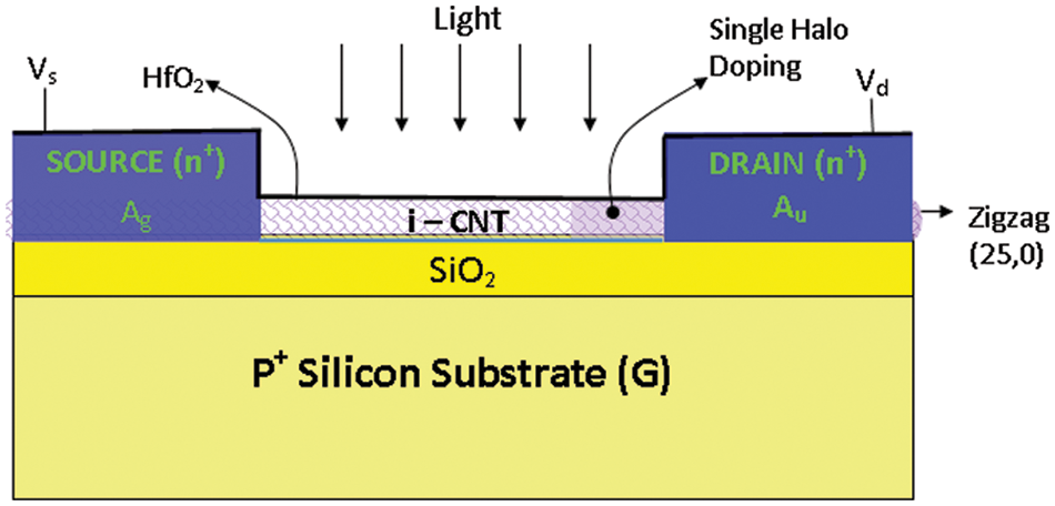
Figure 1: Cross-sectional view of an SH-CNTFET
In the proposed planar SH-CNTFET structure, zigzag (n = 25, m = 0) chirality semiconductor type CNT is used, and the diameter of CNT (dcnt) is 1.95 nm. The energy band gap is 0.4401 eV, and the CNT bridges two electrodes. The layers are the source (Ag) and drain (Au) and are coupled with a thin layer of HfO2, with an insulating oxide thickness (tox) of 1.4 nm and a high dielectric constant (k) of 30. The device dimensions for the structures include a gate (back-gated) length (Lg) of 15 nm and an undoped channel length (Lc) of 10 nm. The source length (Ls) and drain length (Ld) are 20 nm each. Silver metal (Ag = 4.2–4.5 eV) is used at the source, and gold metal (Au = 5.3 eV) is used at the drain. The n+ source and drain doping density are 1.5 × 107 cm−1. The carbon atom density of (4 n/3 acc) in CNTFET, which is 100 nm−1, is compared with the above doping concentration. The length of the undoped or intrinsic CNT (i-CNT) channel is 10 nm. The channel consists of a single halo p-doped CNT region with a length of Lshd. The halo doping is done at the drain end. The length of the halo-doped region on the drain side of the Single Halo-Carbon Nano Tube Field Effect Transistor (SH-CNTFET) is Lshd = 5 nm, and the doping concentration is Nshd = 1.2 nm−1. Except for halo doping, the values of the Single Halo CNTFET and C-CNTFET Device Parameters are equal. Vg is a gate-controlled voltage, while Vd and Vs are the drain and source voltages applied to the SH-CNTFET. The prime focus of the proposed SH-CNTFET simulation is on the characteristic study in dark and illuminated conditions with light incident power Popt = 100 W/cm2 and photon energy of 2.72 eV. Wavelength (λ) = 456 nm.
3 Quantum Simulation of SH-CNTFET
The proposed model is implantation, which has already established that SCEs can be reduced and achieved in a single-halo CNTFET. Hence, the SH-CNTFET photodetector has been modelled using a two-dimensional (2-D) quantum simulation. The gain, output and transconductance characteristics, cut-off frequency, responsivity and directivity of SH-CNTFET have been obtained by solving, under open boundary conditions, the Schrodinger and 2-Dimensional Poisson equations using self-consistent methods. This solution has been received within Green’s function (NEGF) framework. In this simulation of SH-CNTFET done under room temperature, below are the locations of the Fermi levels. The valence band Ag is set at the top, and the Fermi level Au is set for the conduction band. At the junction between the metal and SH-CNTFET is the electron-electron coupling and the photon-electron coupling, described in Green’s function equations with their self-energies. The excitonic effect can be neglected in the given simulation. Even though uneven metal contacts result in doping, this neglect is reasonable. The I-V characteristics are obtained by the self-consistent solution of the Poisson equations and Green function. The simulation process is detailed in the steps below. The Green’s function for the given device is given by
In Eq. (1), E denotes energy, and infinitesimal broadening is denoted by
The Hamiltonian matrix can be calculated as
where b2q = tcos (q/n), t = 3 eV, n is the chirality vector of the nanotube, q is the angular quantum number, N is the total number of carbon rings along the device, and t is the potential for the interaction of two adjacent positions in the network. The total number of carbon atoms is N. The size of the Hamiltonian matrix is N × N.
The self-energy
The electron-photon coupling generates the broadening function, which is given by
In the above equation, j is the layer count of the grid slice.
The Correlation function of the hole and electron in the Eq. (4) can be written as
where
The back gate SH-CNTFET’s self-consistent electrostatic potential (U) in Eq. (1) can be calculated using a two-dimensional Poisson equation. The value of the potential for the Poisson equation can be given as
where
where
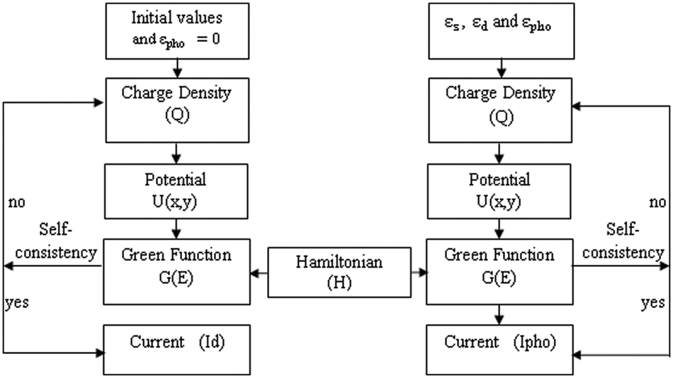
Figure 1a: The process of current calculation for dark and illuminated conditions
In the simulation of self-consistency, the dark current (Id) is calculated using the following steps: In the first step, assign the value
The current in dark conditions is calculated by
where h is the Plank’s constant, q is the electron charge,
Self-consistent photocurrent can be calculated using the following steps. At the start, the initial values are derived from Eqs. (5) and (6). The values in the dark conditions for
Fig. 2 shows the simulation results of the current drain characteristics of the zigzag (25, 0) semiconductor CNT. Where Vgs = 1.2 V, Popt = 100 W/cm2, photon energy is 2.72 eV. tox = 1.4 nm, and wavelength (λ) = 456 nm. At Vds 0.8 V, the current increases linearly and reaches a saturated state. It is observed that the Iph of SH-CNTFET is larger than the dark current (Id) of SH-CNTFET. The latter is lower when the Ioff of C-CNTFET and the SH-CNTFET are compared. Thus, the drain current of the Single Halo CNTFET is higher than C-CNTFET. The leakage current decreases in SH-CNTFET, and the on-off current ratio increases when compared to C-CNTFET [25]. Thus, the SH-CNTFET structure can do the following. The ON/OFF current ratio is increased. The structure demonstrates that the gate controls the channel and, finally and more importantly, improves the switching speed. The proposed device has a high switching speed, which makes it ideal for high-speed and high-frequency circuits [12]. The drop in conductance at the drain for SH-CNTFET and a rise in transconductance are obtained in the case of SH-CNTFET. Then the transconductance of the SH-CNTFET is 7.8 × 10⁻⁵ mho.
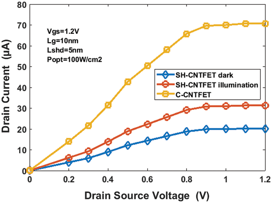
Figure 2: Drain current characteristic at Vgs = 1.2 V, Popt = 100 W/cm2, wavelength (λ) = 456 nm under dark and illumination conditions
SH-CNTFET and C-CNTFET do not coincide. However, with the single halo-doped at the drain side, the dark current of SH-CNTFET is significantly decreased. It proves that the lowest off-state current is mainly attributed to the single halo structure. Fig. 3 shows the potential value in the surface’s length of single haloCNTFET and C-CNTFET structures having Vgs = 1 V, Popt = 100 W/cm2 and a wavelength of 456 nm (2.72 eV). Fig. 3 shows that the single halo CNTFET structure has a potential in the length of the channel that has sudden changes. The variation in drain potential does not affect the area of the SH-CNTFET where it is p-doped. That is to say, the drain current, once saturated, is not affected by the drain potential. Drain-induced barrier lowering (DIBL) is reduced significantly.
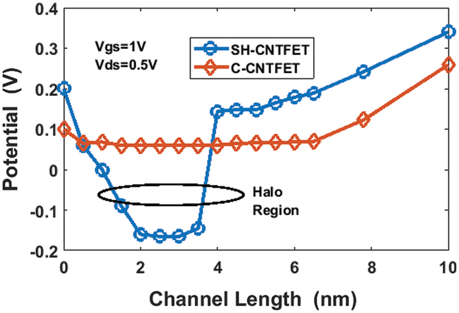
Figure 3: Potential along the surface of the SH-CNTFET structure at Vgs = 1 V, Popt = 100 W/cm2, wavelength (λ) = 456 nm under dark and illumination conditions
Fig. 4 shows the sub-threshold swing of the Single Halo CNTFET and C-CNTFET at Vgs = 0.5 V, Vds = 1 V, and Popt = 100 W/cm2 in dark and illumination conditions. In CMOS circuits, the standby power dissipation is increased, and the factor contributing to this is the sub-threshold leakage. The theoretical sub-threshold swing is 60 mV/decade at room temperature. This applies to CNTFETs, sub-threshold swings of SH-CNTFET and C-CNTFET at Vgs = 0.5 V and compared in Fig. 4. From Fig. 4, it is evident that when comparing single halo CNTFET with C-CNTFET, the former shows sub-threshold swing. Concerning the smallness of DIBL and the swing of the SH-CNTFET, the proposed SH-CNTFET structure offers better control of Short Channel Effects [25].
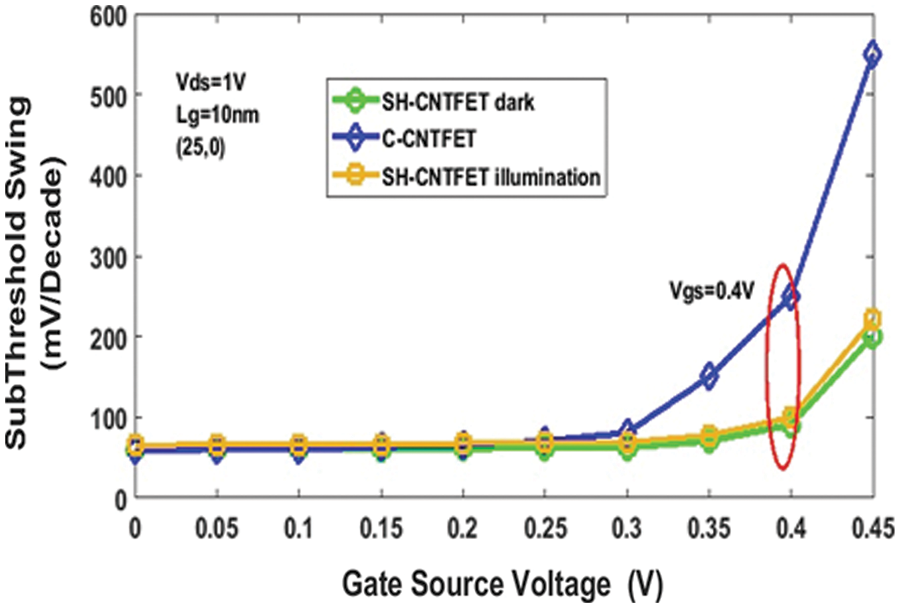
Figure 4: Sub-threshold swing of SH-CNTFET and C-CNTFET with Vgs = 0.5 V, Vds = 1 V, Popt = 100 W/cm2, wavelength (λ) = 456 nm under dark and illumination conditions
Fig. 5 shows the transconductance characteristics of the SH-CNTFET and C-CNTFET structures at Popt = 100 W/cm2, Vds = 1 V. The simulation is obtained by varying the gate-source voltage from 0 to 1 V, noting and comparing the corresponding current value with C-CNTFET. Then the current is initially there is no increment, and then after 0.5 V, it is increased. The current in illuminated conditions for single halo CNTFET is lower than that for C-CNTFET. This is caused by the increased threshold voltage of the single halo CNTFET and reduced drain conductance. Comparison of the C-CNTFET and SH-CNTFET and the on-off current ratio (Ion/Ioff) results in the observation that the on-off current of the SH-CNTFET is significantly larger. Moreover, the transconductance (gm) is increased for SH-CNTFETs. Fig. 4 shows that the drain conductance of the SH-CNTFET is reduced [12]. At Vgs = 0.7 V, the transconductance of the SH-CNTFET is 7.8 × 10⁻⁵ mho, which is higher than that of the C-CNTFET. The output conductance is 2.8 × 10⁻⁶ S.
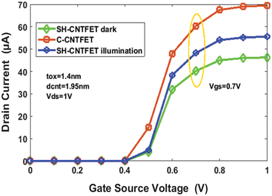
Figure 5: Tranconductance of the SH-CNTFET and C-CNTFET with Vgs = 1 V, Vds = 1 V, Popt = 100 W/cm2, wavelength (λ) = 456 nm under dark and illumination conditions
Fig. 6 shows the relationship between the cut-off frequency and the gate-source voltage at 0.8 V. The doping profile of the drain and source of this device achieves the increase of gm and decrease of channel charge variation vs. gate-source voltage. The gate length of both the C-CNTFET and SH-CNTFET achieves terahertz level cut-off frequencies. A higher cut-off frequency is observed in the halo structure for a fixed gate length. Fig. 5 shows the higher transconductance achieved [12]. As a result, as observed below, there is an increase in the cut-off frequency characteristic. In addition, the cut-off frequency of the SH-CNTFET is 6.45 THz compared to the CNTFET structure, which is 4.3 THz. Fig. 7 shows the gain of SH-CNTFET with various diameters from 0.5 to 2 nm at Popt = 100 W/cm2. To achieve a relatively large transconductance, the SH-CNTFET must have a large channel diameter. A minimised hot carrier effect is observed due to a reduction in the peak of the electric field at the drain side. There is a significant increase in the voltage gain [23]. This effect is due to the drastic reduction in the drain conductance of the HD-CNTFET. The larger the transconductance, the greater the gain it will deliver. Consequently, the voltage gain is higher when a nanotube has a larger diameter. The gain of SH-CNTFET is 28.55 db when the diameter of the CNT is set at 1.9 nm. Hence, it can be derived that the lower bandgap is obtained from the (25, 0) chirality semiconductor type CNT. Fig. 8 shows directivity being proportional to the bias voltage, and the directivity of SH-CNTFET at Popt is 100 W/cm2. The directivity of SH-CNTFET is 9.4 cmHz−1/w at Vgs = 2 V and Vds = 1 V. The proposed SH-CNTFET photodetector’s efficiency is calculated at Popt = 100 W/cm2 and a wavelength of 456 nm. The photons hit the SH-CNTFET photo’s surface and produced the photo-excited electron-hole pairs. The responsivity of the proposed SH-CNTFET is 105.48 mA/W, and the efficiency is 75%. Fig. 9 shows the energy band diagram of Au and CNT. The Au-CNT in the SH-CNTFET device improves the performance of the phototransistor through proper doping.
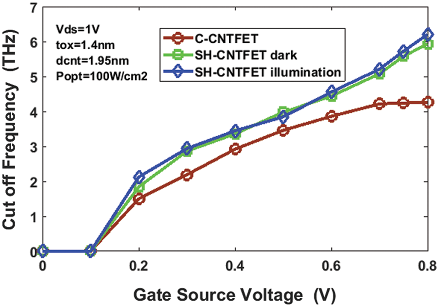
Figure 6: Cut-off Frequency of the SH-CNTFET and C-CNTFET with Vgs = 1 v, Popt = 100 W/cm2, wavelength (λ) = 456 nm under dark and illumination conditions
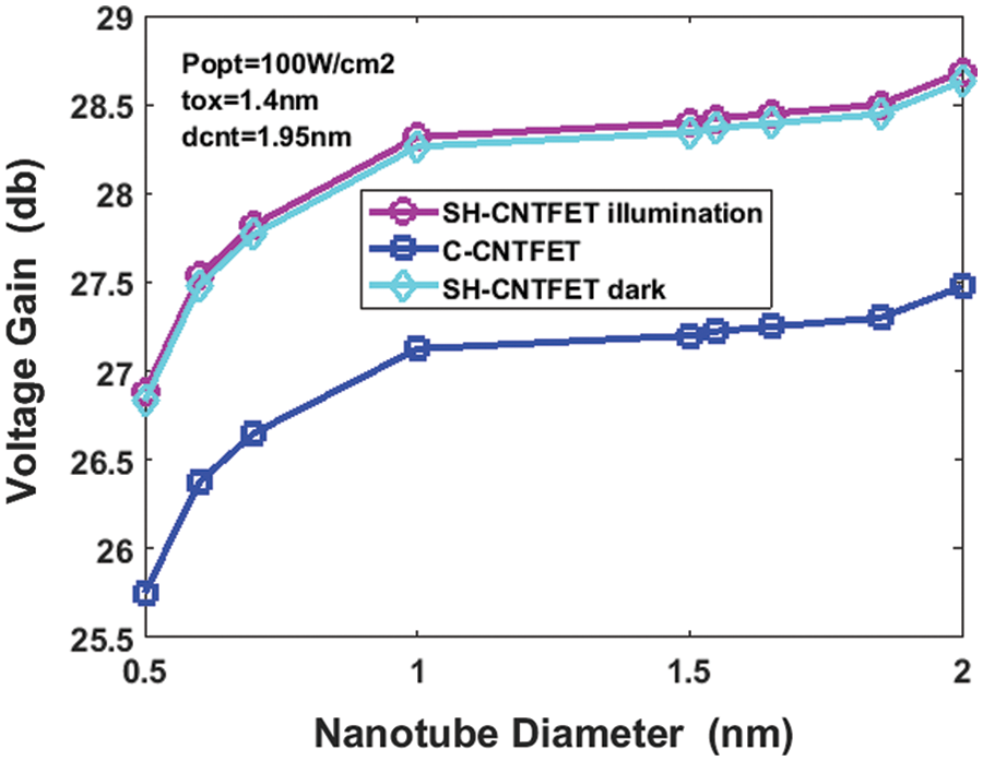
Figure 7: Gain of the SH-CNTFET structure with Vds = 1, Popt = 100 W/cm2, wavelength (λ) = 456 nm under dark and illumination conditions
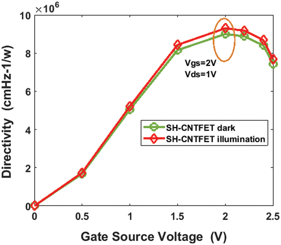
Figure 8: Directivity of SH-CNTFET with Popt = 100 W/cm2, wavelength (λ) = 456 nm under dark and illumination
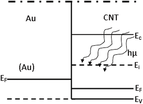
Figure 9: Energy level of Au and CNT
Table 2 compares the SH-CNTFET with other CNTFET devices at Vds = 0.5 V. The sensitivity of the CNT is evaluated at varying visible wavelengths. The light intensity of 456 nm is applied, and the SH-CNTFET’s dependence on light intensity is evaluated. The efficiency of the proposed SH-CNTFET devices is observed only in visible light. At the minimum optical incident, with a power of 100 W/cm2, it produces better photocurrent when compared with other photo devices such as CNTFET and SWCNT array. When the device is exposed to visible light, photons with higher energy than the CNT’s band gap will generate electron-hole pairs and separate the depletion region between metal and CNT to produce photocurrent. In addition, the directivity and responsivity of the SH-CNTFET are significantly increased compared to the SWCNT array. Good sensitivity is observed in the absorption spectrum of the proposed SH-CNTFET and the absorption of visible light.
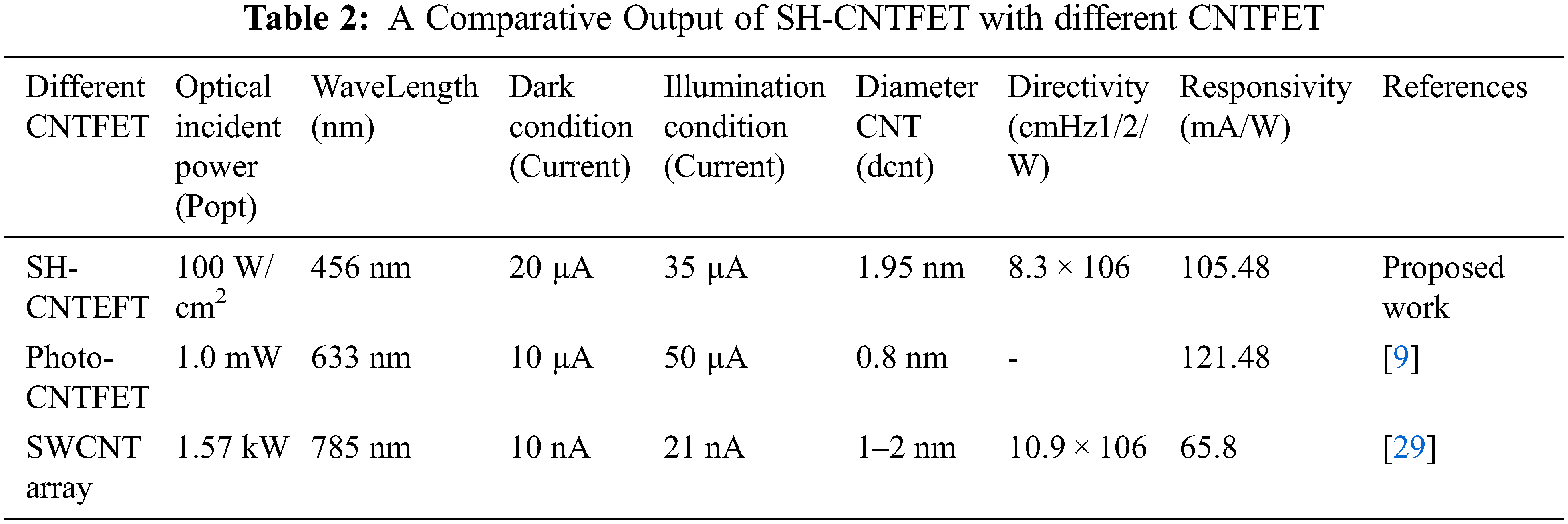
Table 3 shows the comparison of the SH-CNTFET and DGM-CNFET photodetectors. The diameter of the DMG-CNTFET device is smaller than the proposed SH-CNTFET device. The table shows that increasing the halo doping causes a decrease in conductance. The proposed SH-CNTFET device has these advantages: it provides higher transconductance, cut-off frequency, and gain than the DMG-CNTFET device. Lg = 10 nm, which is considered to be a fixed undoped channel Length and Lshd = 5 nm, which is the length of halo doping. The electrical characteristics of SH-CNTFETs are evaluated in terms of current drain characteristics, transconductance, and sub-threshold swing as a function of parameter values.
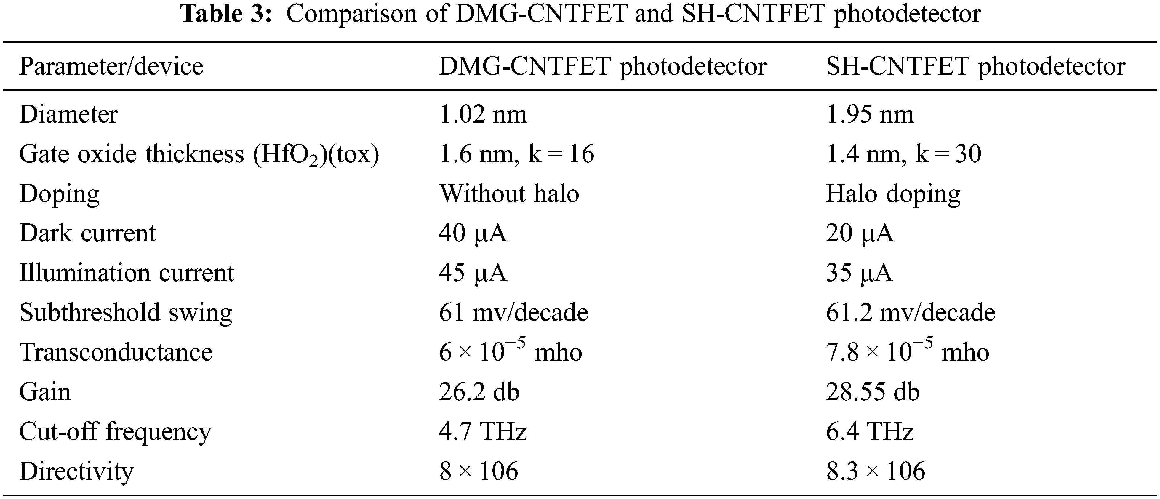
Table 3 compares the DMG-CNTFET and the SH-CNTFET, proving that the dark current is just 20 μA for the latter method and is better than the previous DMG CNTFET. The SH-CNTFET advances the DMG-CNTFET in sub-threshold swing, transconductance, gain, cut-off frequency and directivity.
The SH-CNTFET photodetector proposed in this paper is a single halo-doped with a single gate material of Au, a larger zigzag and smaller energy band gap and a HfO2 dielectric. The above modifications help achieve reduced leakage current, increased Ion/Ioff ratio, increased cut-off frequency, and increased transconductance and quantum efficiency. The achieved results have also been compared to existing CNTFETs and found to have improved performance. The method used for the characteristic study is found to provide more accurate results. The simulation is achieved through the solution of the Green function method for the SH-CNTFET photodetector under dark and illuminated conditions. The latest technology innovations requiring speed, switching, accuracy and reliability need devices that support such complexity. Also, as the technology is moving into optical innovations, photodetectors such as the proposed device with quantum efficiency are more crucial. In the future, a simulation of the noise analysis of the carbon nanotube FET photodetector can be carried out.
Funding Statement: The authors received no specific funding for this study.
Conflicts of Interest: The authors declare that they have no conflicts of interest to report regarding the present study.
References
1. A. Naderi, M. Ghodrati and S. Baniardalani, “The use of a Gaussian doping distribution in the channel region to improve the performance of a tunneling carbon nanotube field-effect transistor,” Journal of Computational Electronics, vol. 19, no. 1, pp. 283–290, 2020. [Google Scholar]
2. A. Singh, S. Chaudhary, S. M. Sharma and C. K. Sarkar, “Improved drive capability of silicon nano tube tunnel FET using halo implantation,” Silicon, vol. 12, no. 11, pp. 2555–2561, 2020. [Google Scholar]
3. A. Pacheco-Sanchez and M. Claus, “Bias-dependent contact resistance characterization of carbon nanotube FETs,” IEEE Transactions on Nanotechnology, vol. 19, pp. 47–51, 2020. [Google Scholar]
4. R. Goel, C. Gupta and Y. S. Chauhan, “Analysis and compact modeling of thermal noise in halo implanted MOSFETs,” in Proc. 4th Electron Devices Technology & Manufacturing Conf. (EDTM), Penang, Malaysia, IEEE, pp. 1–4, 2020. [Google Scholar]
5. A. Tijjani, G. S. M. Galadanci and G. Babaji, “Drain current characteristics of carbon-nanotube FET (CNTFET) with SiO2, ZrO2 and HfO2 as dielectric materials using FETToy code,” NIPES Journal of Science and Technology Research, vol. 2, pp. 212–227, 2020. [Google Scholar]
6. M. K. Anvarifard, “Modeling a double-halo-doping carbon nanotube FET in DC and AC operations,” ECS Journal of Solid State Science and Technology, vol. 7, no. 12, pp. M209, 2018. [Google Scholar]
7. A. G. N. Raeini and Z. Kordrostami, “Modified schottky barrier CNTFET with lightly doped drain,” Micro & Nano Letters, vol. 13, no. 4, pp. 442–447, 2018. [Google Scholar]
8. C. Gupta, H. Agarwal, S. Dey, C. Hu and Y. S. Chauhan, “Analysis and modeling of capacitances in halo-implanted MOSFETs,” in Proc. Electron Devices Technology and Manufacturing Conf. (EDTM), Toyama, Japan, IEEE, pp. 198–200, 2017. [Google Scholar]
9. A. Mahmoudi, M. Troudi, P. Bondavalli and N. Sghaier, “Comparison of the quantum efficiency and the responsivity of the single-walled carbon nanotube photodetector with different electrode metals,” Journal of Materials Science, vol. 52, no. 17, pp. 10273–10284, 2017. [Google Scholar]
10. M. A. Eshkalak and M. K. Anvarifard, “A guideline for achieving the best electrical performance with strategy of halo in graphene nanoribbon field effect transistor,” ECS Journal of Solid State Science and Technology, vol. 5, no. 12, pp. M141, 2016. [Google Scholar]
11. A. Naderi, “Double gate graphene nanoribbon field effect transistor with single halo pocket in channel region,” Superlattices and Microstructures, vol. 89, pp. 170–178, 2016. [Google Scholar]
12. W. Wang, H. Wang, J. Liu, N. Li, T. Zhang et al., “Performance analysis of an ultralow power circuit using single halo CNTFETs,” Semiconductor Science and Technology, vol. 30, no. 5, pp. 055018, 2015. [Google Scholar]
13. F. Mozahid and M. T. Ali, “Simulations of enhanced CNTFET with HfO2 gate dielectric,” International Journal of Scientific and Research Publications, vol. 5, no. 3, pp. 1–6, 2015. [Google Scholar]
14. W. Wang, L. Zhang, X. Wang, Z. Wang, T. Zhang et al., “The combined effects of halo and linear doping effects on the high-frequency and switching performance in ballistic CNTFETs,” Journal of Semiconductors, vol. 35, no. 11, pp. 114004, 2014. [Google Scholar]
15. W. Wang, N. Li, C. Xia, G. Xiao, Y. Ren et al., “Quantum simulation study of single halo dual-material gate CNTFETs,” Solid-State Electronics, vol. 91, pp. 147–151, 2014. [Google Scholar]
16. M. J. Hejazifar and S. A. SedighZiabari, “Investigation of the cutoff frequency of double linear halo lightly doped drain and source CNTFET,” International Nano Letters, vol. 4, no. 3, pp. 1–5, 2014. [Google Scholar]
17. V. Thirunavukkarasu, K. Priyadharsini, P. A. Priya and D. J. Thiruvadigal, “Modelling and simulation of carbon nanotubes (CNT) for nanoelectronics device applications,” in Proc. Int. Conf. on Information Communication and Embedded Systems (ICICES), Chennai, India, IEEE, pp. 1027–1029, 2013. [Google Scholar]
18. S. Farhana, A. Z. Alam, S. Khan and S. M. A. Motakabber, “Modeling of small band-gap CNT for designing of faster switching CNTFET,” in Proc. Business Engineering and Industrial Applications Colloquium (BEIAC), Langkawi, Malaysia, IEEE, pp. 589–592, 2013. [Google Scholar]
19. A. Naderi and P. Keshavarzi, “Novel carbon nanotube field effect transistor with graded double halo channel,” Superlattices and Microstructures, vol. 51, no. 5, pp. 668–679, 2012. [Google Scholar]
20. B. Syamal, C. Bose, C. K. Sarkar and N. Mohankumar, “Effect of single HALO doped channel in tunnel FETs: A 2-D modeling study,” in Proc. Int. Conf. of Electron Devices and Solid-State Circuits (EDSSC), Hong Kong, China, IEEE, pp. 1–4, 2010. [Google Scholar]
21. C. Chen, W. Zhang, E. S. W. Kong and Y. Zhang, “Carbon nanotube photovoltaic device with asymmetrical contacts,” Applied Physics Letters, vol. 94, no. 26, pp. 263501, 2019. [Google Scholar]
22. A. A. Orouji and S. A. Ahmadmiri, “Novel attributes and design considerations of source and drain regions in carbon nanotube transistors,” Physica E: Low-Dimensional Systems and Nanostructures, vol. 42, no. 5, pp. 1456–1462, 2010. [Google Scholar]
23. Z. Arefinia and A. A. Orouji, “Novel attributes in scaling issues of carbon nanotube field-effect transistors,” Microelectronics Journal, vol. 40, no. 1, pp. 5–9, 2009. [Google Scholar]
24. Z. Arefinia and A. A. Orouji, “Novel attributes in the performance and scaling effects of carbon nanotube field-effect transistors with halo doping,” Superlattices and Microstructures, vol. 45, no. 6, pp. 535–546, 2009. [Google Scholar]
25. Z. Arefinia, “Investigation of the performance and band-to-band tunneling effect of a new double-halo-doping carbon nanotube field-effect transistor,” Physica E: Low-Dimensional Systems and Nanostructures, vol. 41, no. 10, pp. 1767–1771, 2018. [Google Scholar]
26. Z. Arefinia and A. A. Orouji, “Impact of single halo implantation on the carbon nanotube field-effect transistor: A quantum simulation study,” Physica E: Low-Dimensional Systems and Nanostructures, vol. 41, pp. 196–201, 2008. [Google Scholar]
27. A. Singh, C. K. Pandey, S. Chaudhury and C. K. Sarkar, “Tuning of threshold voltage in silicon nano-tube FET using halo doping and its impact on analog/RF performances,” Silicon, vol. 13, no. 11, pp. 3871–3877, 2021. [Google Scholar]
28. A. Karimi and A. Rezai, “A design methodology to optimize the device performance in CNTFET,” ECS Journal of Solid State Science and Technology, vol. 6, no. 8, pp. 97–110, 2017. [Google Scholar]
29. Q. Zeng, S. Wang, L. Yang, Z. Wang, T. Pei et al., “Carbon nanotube arrays based high-performance infrared photodetector,” Optical Materials Express, vol. 2, no. 6, pp. 839–848, 2012. [Google Scholar]
Cite This Article
 Copyright © 2023 The Author(s). Published by Tech Science Press.
This work is licensed under a Creative Commons Attribution 4.0 International License , which permits unrestricted use, distribution, and reproduction in any medium, provided the original work is properly cited.
 Downloads
 Citation Tools