 Submit a Paper
 Propose a Special lssue
 Open Access
ARTICLE

Detection Algorithm of Surface Defect Word on Printed Circuit Board
School of Computer Engineering, Jiangsu University of Technology, Changzhou, 213001, China
* Corresponding Author: Min Zhang. Email:
Computer Systems Science and Engineering 2023, 46(3), 3911-3923. https://doi.org/10.32604/csse.2023.036709
Received 10 October 2022; Accepted 24 February 2023; Issue published 03 April 2023
 View Full Text
 Download PDF
Abstract
For Printed Circuit Board (PCB) surface defect detection, traditional detection methods mostly focus on template matching-based reference method and manual detections, which have the disadvantages of low defect detection efficiency, large errors in defect identification and localization, and low versatility of detection methods. In order to further meet the requirements of high detection accuracy, real-time and interactivity required by the PCB industry in actual production life. In the current work, we improve the You-only-look-once (YOLOv4) defect detection method to train and detect six types of PCB small target defects. Firstly, the original Cross Stage Partial Darknet53 (CSPDarknet53) backbone network is preserved for PCB defect feature information extraction, and secondly, the original multi-layer cascade fusion method is changed to a single-layer feature layer structure to greatly avoid the problem of uneven distribution of priori anchor boxes size in PCB defect detection process. Then, the K-means++ clustering method is used to accurately cluster the anchor boxes to obtain the required size requirements for the defect detection, which further improves the recognition and localization of small PCB defects. Finally, the improved YOLOv4 defect detection model is compared and analyzed on PCB dataset with multi-class algorithms. The experimental results show that the average detection accuracy value of the improved defect detection model reaches 99.34%, which has better detection capability, lower leakage rate and false detection rate for PCB defects in comparison with similar defect detection algorithms.Keywords
As the industrial industry upgrades and iterates, the emerging 3C products are novel in style and diverse in variety. PCB is the basic carrier of electronic equipment, on which a large number of components are placed, and the quality of PCB will directly affect the performance of electronic equipment. In order to avoid the shortcomings of manual detection, easy fatigue and low efficiency, Automated Optical Inspection (AOI) based on machine vision has been widely used in industry, As PCBs types become more complex, the task of detecting and classifying defects is more difficult than ever [1,2]. Traditional AOI detection of PCBs can be divided into three main streams, including the reference comparison method, the non-reference verification method and the hybrid method. In the reference comparison method, a standard image called a template is prepared, and then the PCB to be inspected is compared with the template to find out the unknown defects. Although it is straightforward and easy to use, there are many factors that we must consider, including unbalanced illumination, inaccurate registration, and large amounts of storage [3,4]. In the non-reference verification method, the purpose of the method is to find out if the wiring tracks, pads and holes meet the design requirements without a template. This method does not have the limitations of reference method.
However, it may have difficulties in detecting large defects. In the hybrid method, the reference and non-reference methods are combined, and this method will have the advantages of two basic methods, however, it requires high computational power and suffers from localization position error instability. Deep learning defect detection algorithm with its strong computational power has a better solution to the low accuracy, low stability and low real-time and does not require the use of template matching for PCB defect detection. Moreover, as a novel Nondestructive Testing and Evaluation (NDT&E) technique, infrared thermography based on thermal diffusion mechanism was widely employed to monitor several objects [5], among which electronic PCBs. For an optical welding inspection, a demand-actuated NDT&E can be carried out by using automated in-line systems, including the selection of suitable cameras, the correction of perspective-based distortion of the images and a suitable experimental setup [6]. Lock-in thermography is the most used infrared detection techniques owing to good detection effect and large depth detection ability. Infrared thermal camera can be chosen to detect the temperature distribution of PCBs under electric loading, and the power loss of components was used to analyze the temperature distribution. With the development of large-scale integrated circuits, multi-layer complex structure and multi-type characteristic of PCBs are the major challenge to accurate detection for lock-in thermography.
At present, there are more defect detection algorithms and outstanding performance, and more widely used PCB defect detection methods are YOLO series network as the representative of the one stage defect detection algorithm. The Region Convolutional Neural Network (R-CNN) series serve as the representative of the second stage defect detection method. The difference between both is mainly reflected in whether the defect detection task is divided into two categories of classification and regression, YOLO series detection algorithm with high detection speed and good defect detection accuracy in industrial detection has a good universal effect, and YOLOv4 defect detection model has a good balance of defect detection accuracy and detection speed, so we chose it as the PCB defect detection model [7,8]. However, the original YOLOv4 defect detection model has a high false detection rate and leakage rate for high-resolution small target defects, which is not a good task for defect detection in the industrial production process with high accuracy and high detection rate.
Therefore, in this paper, based on the original YOLOv4 defect detection by retaining the original CSPDarknet53 as the backbone network for defect feature extraction, the multi-layer fusion original PA-Net module is modified by attention mechanism processing. Multi-layer feature fusion aims to achieve the integration of global semantic information and underlying location information. The original three YOLO Head are processed as a whole single output by the above operation, and the location information, confidence and type required for defect detection are obtained in these YOLO Head.
In addition, in order to further improve the feature extraction capability of the defect detection network, the detection effect is further improved by using K-means++ for accurate clustering of the anchor boxes. Through the above operation processing, the obtained improved YOLOv4 defect detection network has a better fusion effect on the high-level semantic information and the underlying location information. The defect detection model has a better detection performance for small target defects, and this paper effectively improves the detection accuracy of the detection model for PCB defect data.
The overall structure of this paper is as follows. In Section 1, the paper details the development history and status of PCB defect detection technology and presents the advantages and disadvantages of each type of defect detection technology and the feasibility and effectiveness of the PCB defect detection study conducted in this paper. In Section 2, the advantages of the required defect detection model are described in detail and the improvements of the network over previous versions are presented. In Section 3, the improved network structure is explained detailed.
The contributions of this paper are as follows. At first, the original CSPDarknet53 backbone network is preserved for PCB defect information extraction, and second, the original multi-layer cascade fusion approach is changed to a single-layer feature layer structure to greatly avoid the problem of uneven distribution of anchor boxes sizes during PCB defect detection. Then the K-means++ clustering method is used to accurately cluster the anchor boxes to obtain the required size requirements for the defect detection, thus further improving the recognition and localization of small PCB defects.
The YOLOv4 defect detection network used in this paper mainly consists of a backbone network layer for defect feature extraction, a Neck part for fusion of semantic information between high and low layers, and a Head layer for defect identification and localization. The original YOLOv4 backbone network design idea is mainly based on YOLOv3, where the original Darknet53 and Cross Stage Partial Network (CSP-Net) are fused to achieve efficient extraction capability for feature information, and the original pyramid structure for features is modified to Spatial Pyramid Pooling Network (SPP-Net) structure and Path Aggregation Network (PA-Net) to achieve the fusion of multi-scale features. Multi-scale problem can be handled with image pyramid, where image is re-scaled to different size. The above improvement is essentially through the essence that achieving the augmentation of the perceptual field for defect detection network by SPP-Net and the aggregation process for multipath network by PA-Net, and retaining the original detection method in YOLOv3 in the defect detection part of YOLO Head. This research performed the above network improvement to make the network model with higher detection performance, and it compared to the YOLOv3 method with relatively good performance.
3 Improved YOLOv4 Network Structure
The original YOLOv4 defect detection algorithm maintains the same output structure as YOLOv3 in the defect detection prediction part. These output structures are mainly used to identify and locate PCB defects with uneven defect area distribution, where the PCB size distribution presents three types of sizes, including large, medium and small size types. The YOLO series algorithms is more dependent on reasonable anchor boxes size due to it has good detection results for defects with different sizes [9–11].
In practical industrial applications, the data set to be detected is not likely to reach the ideal state and the defects to be detected are generally of different sizes and randomly distributed in natural state. And the randomness has an impact on the detection effect of YOLOv4. The clustering algorithm is used to cluster the data with uniformly distributed defect sizes, and the anchor boxes size obtained by this operation is more desirable. During the defect detection process, the anchor boxes size obtained by this operation can detect defects well on almost all output feature layers, which mainly results from that defect detection size that is within the expected range. However, the key to the detection method is just a specific state. Therefore, relying on the original anchor boxes dimensions does not meet the practical needs of PCB defect detection [12,13].
In addition, the distribution of the image size of the defect detection dataset is uneven in this paper, and the actual size of the various defects types is random, and the size of such defects is generally as small as one-tenth of the original image size [14]. Through the original clustering algorithm for the clustering operation of the data in this paper, the size of the obtained anchor boxes cannot be reasonably assigned to the multi-level output feature layers.
To address the above problems, this paper combines feature fusion and attention mechanism to realize the output of single-layer feature map and obtains the anchor boxes size by K-means++ clustering algorithm. For the various data in the PCB defect dataset in this paper, the anchor boxes size assigned to the single-layer feature map has a good match for all types of defect sizes, which solves the drawback that the anchor boxes cannot be reasonably assigned in the original defect detection model. This network improvement method has a higher detection effect for the defect detection model on PCB small target defects. At the same time, compared with the original YOLOv4 network model, the single output structure is more compact in comparison with the previous three-layer output, and the parameter size is about 55% of the original model parameters, which has better results for mobile deployment under the same conditions.
The improved YOLOv4 improvement algorithm retains the original CSPDarkNet53 backbone network for the feature extraction process, and the original PA-Net fusion method in the feature fusion stage is unable to obtain detailed feature information for the sample data processed in this paper, which has a high miss detection rate and false detection rate on PCB small target defect detection. In order to further improve the recognition accuracy of the PCB defect detection model, this paper achieves detailed extraction of feature information by improving the network structure for the feature fusion process, which operates by combining feature fusion with an attention mechanism [15,16].
In defect detection networks, the more commonly applied feature fusion methods include element summation and concatenation methods. The original YOLOv4 network uses the concatenation method to achieve fusion of features at different levels. The specific operation process is as follows. First, in order to achieve the connection of the multi-layer feature layers in the channel dimension, the features of different levels are scaled to the same resolution by means of dimensional deflation, and then they are connected in series in the channel dimension. However, this fusion method is computationally intensive and cannot afford the real-time performance required by the actual industrial production. In order to better meet the requirements of real-time, efficiency and stability in PCB defect detection, this paper tries to use a combination of feature fusion and attention mechanism to reduce the model training time and improve the defect detection efficiency to some extent.
The specific details of the improvement are shown in Fig. 1. During the channel feature fusion stage, the integration of channels is achieved by joining the acquired three feature layers in a concatenated manner. Among them, if the resolution of the feature map to be fused is smaller than the resolution of the target feature map, the problem can be solved by using a reverse convolution layer to enlarge the features, and then using a 1×1 convolution layer to compress the channels to the target range. If the feature map resolution to be fused is larger than the target feature map resolution, we use a 3×3 convolutional layer with a step size of 2 to reduce the feature resolution and channel size.
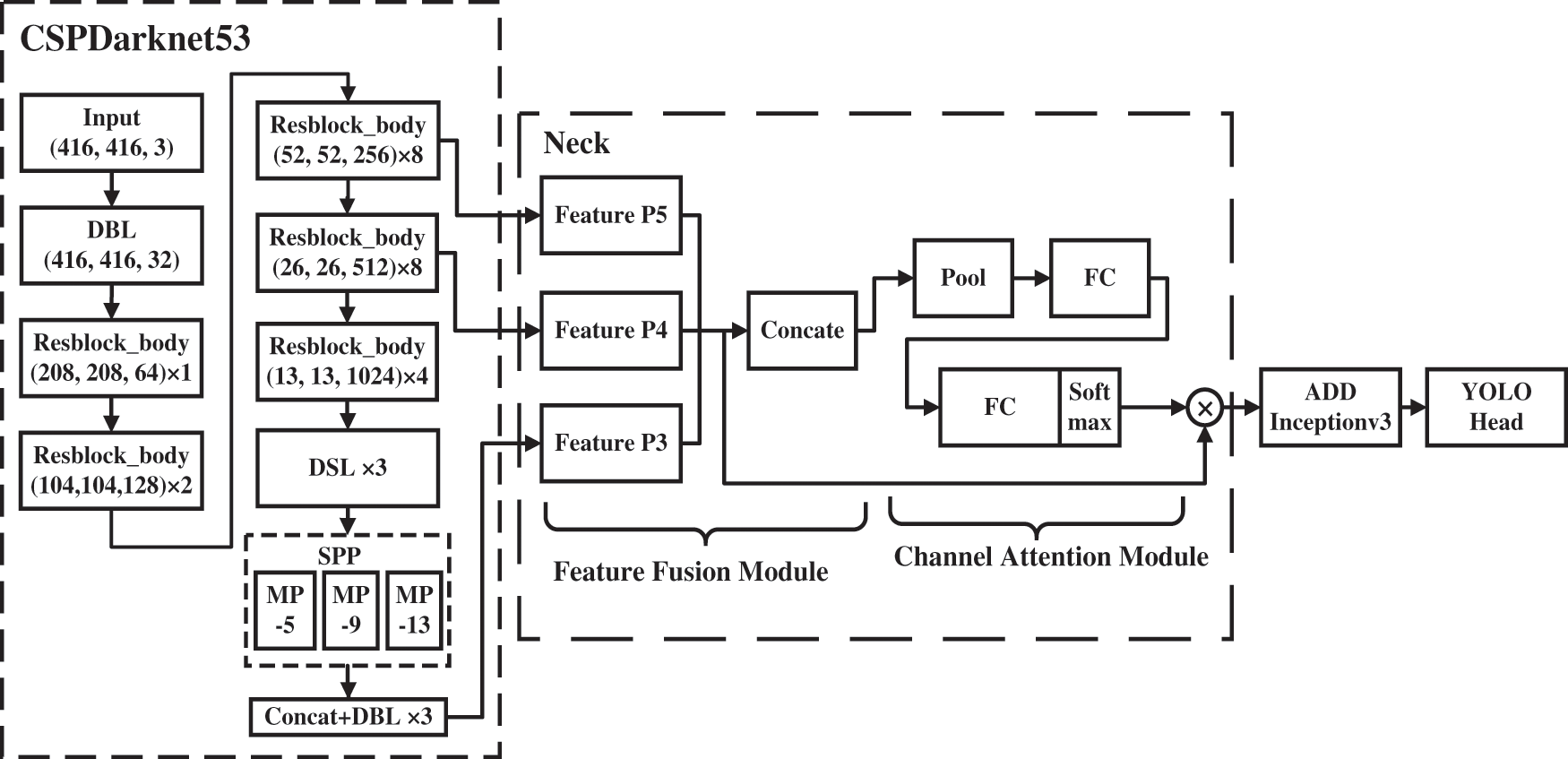
Figure 1: Improved YOLOv4 network structure
Then, this paper generates channel feature vectors by using a global average pooling layer for feature layer deflation, which enables the calibration of the importance of information in each channel. The channel feature vectors obtained by the above operation are processed by a lower dimensional fully connected layer followed, which allows the network model to learn the fusion weights of features at different levels adaptively. In addition, the weight sizes after processing in the fully connected layer are normalized to the features by the soft-max function and the final feature fusion is achieved. In this way, the calibration of the important semantic information contained in each channel and the identification process of important location information can be obtained by virtue of the weight size [17].
In the original YOLOv4 defect detection algorithm, the anchor boxes are obtained by clustering operations on the public dataset-Common Objects in Context (COCO) dataset, and this approach is not applicable to the PCB surface defect detection algorithm performed in this paper. Meanwhile, the original YOLOv4 clustering algorithm uses K-means clustering to obtain the defect height and width dimensions, and this method has obvious defects. The main key is whether the initial clustering center is reasonably positioned [18]. A reasonable clustering operation is the initial clustering center with dispersion characteristics. Only by ensuring randomness and dispersion in the selection of the initial clustering points, the defect detection model can ensure efficient and stable defect detection in the training process.
Therefore, the K-means++ algorithm is used to obtain the initial clustering points in this paper, and the specific principle is to randomly select the sample data from the experimental PCB defect data set as the clustering initial point
According to the above operation to obtain K clustering centroids, and all kinds of samples through the Euclidean clustering calculate the minimum clustering centroid region and update the clustering points, and so on gradually update until the clustering points remain unchanged update end. In the subsequent clustering process, the similarity between the sample prediction bounding box and the real boundary is mainly used for clustering, and the Intersection Over Union (IOU) is usually chosen as the similarity index for the calculation of the similarity between the two boxes in the field of defect detection [19]. The calculated formula is as follows.
In this paper, the number of anchor boxes obtained by the clustering algorithm on the PCB defective dataset is 9. The specific numerical sizes are: (19,16); (32,17); (21,35); (40,31); (32,46); (61,24); (23,65); (50,43); (67,53).
4 Experimental Results and Analysis
The software and hardware environment configurations of the experimental environment in this paper are shown in Tables 1 and 2.
Due to the scarcity of PCB data sets, in order to further verify the outstanding performance of the algorithms in this paper in PCB defect detection, this paper uses the performance of different defect detection algorithms on PCB defect data sets to compare the operation. The specific operation includes the selection of the more common six categories of PCB defect types as the target in this paper, the selected defects mainly include missing hole, mouse bite, open circuit, short, spur, spurious copper 6 categories, as shown in Fig. 2 [20].
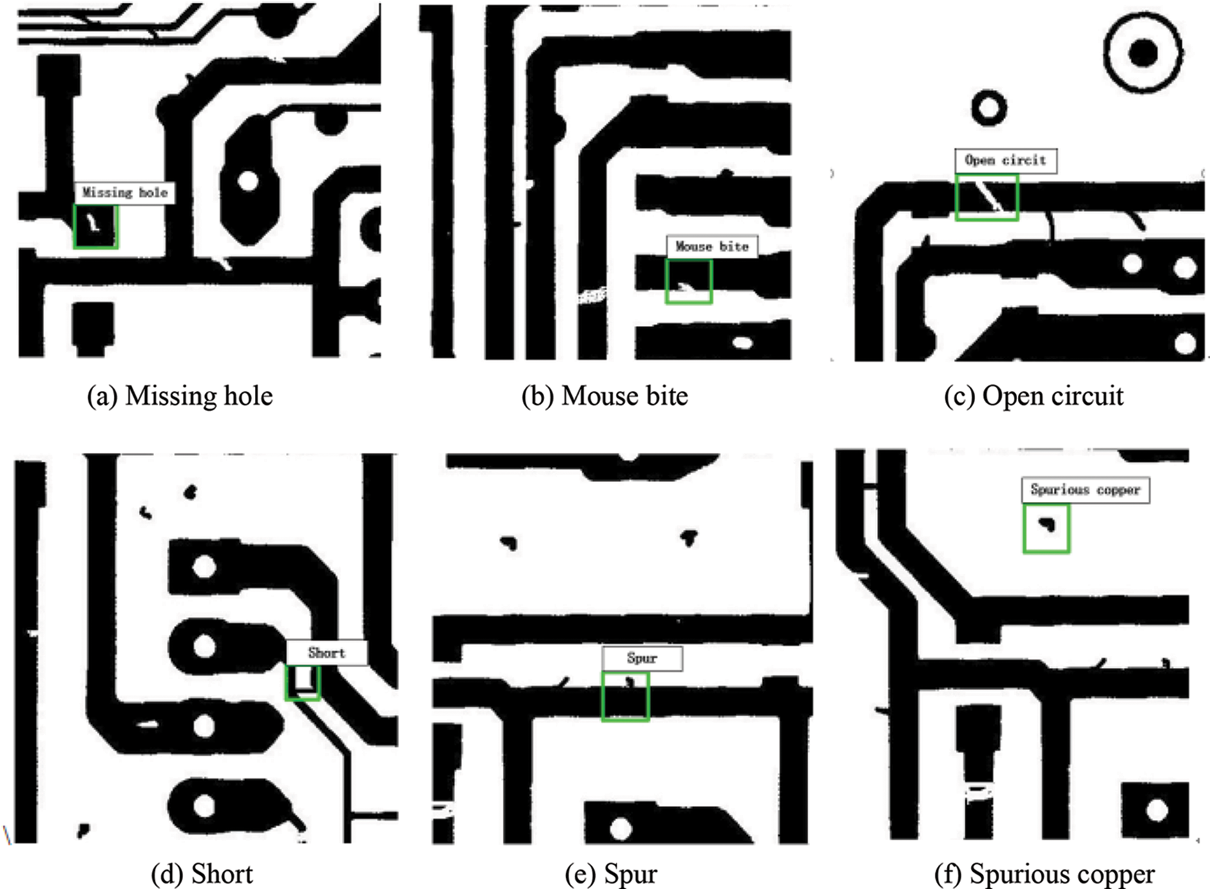
Figure 2: PCB six categories of defects categories
At the same time, considering the uneven number of PCB defect image types, this paper carries out the acquisition of different types of images and augments the training data by means of conventional preprocessing, including cropping, panning, changing the brightness, adding noise, rotating the angle, and mirroring. Through the above operations, the data scale data augmentation can be achieved, and finally the acquired dataset is proportionally distributed as the training dataset and the test dataset with data scales of 9860 and 4530, respectively. The validity and feasibility of the dataset scale can be achieved by the above methods.
The resolution of the PCB defect data set is a large size, fine image, and high quality defect images, but the defect detection model selected in this paper cannot directly detect defects in the original image due to the default defect image input size of 416 × 416 pixels in this network model, so there is a problem of non-conformity between the original image and the supported input image size [21].
In order to ensure that the YOLO detector selected in this paper provides high quality detection of PCB defect data, this paper uses a pre-processing operation represented by cropping method on the above original image to make the acquired sub-image size more reasonable to facilitate the subsequent detection process.
For the acquired experimental sample data set, the final size of the sub-image is set to 416 × 416 pixels, and the overlap area of the sub-image in the cutting process is 20% of the pixel points. This overlap area size can achieve complete retention of various defective areas during the cutting process.
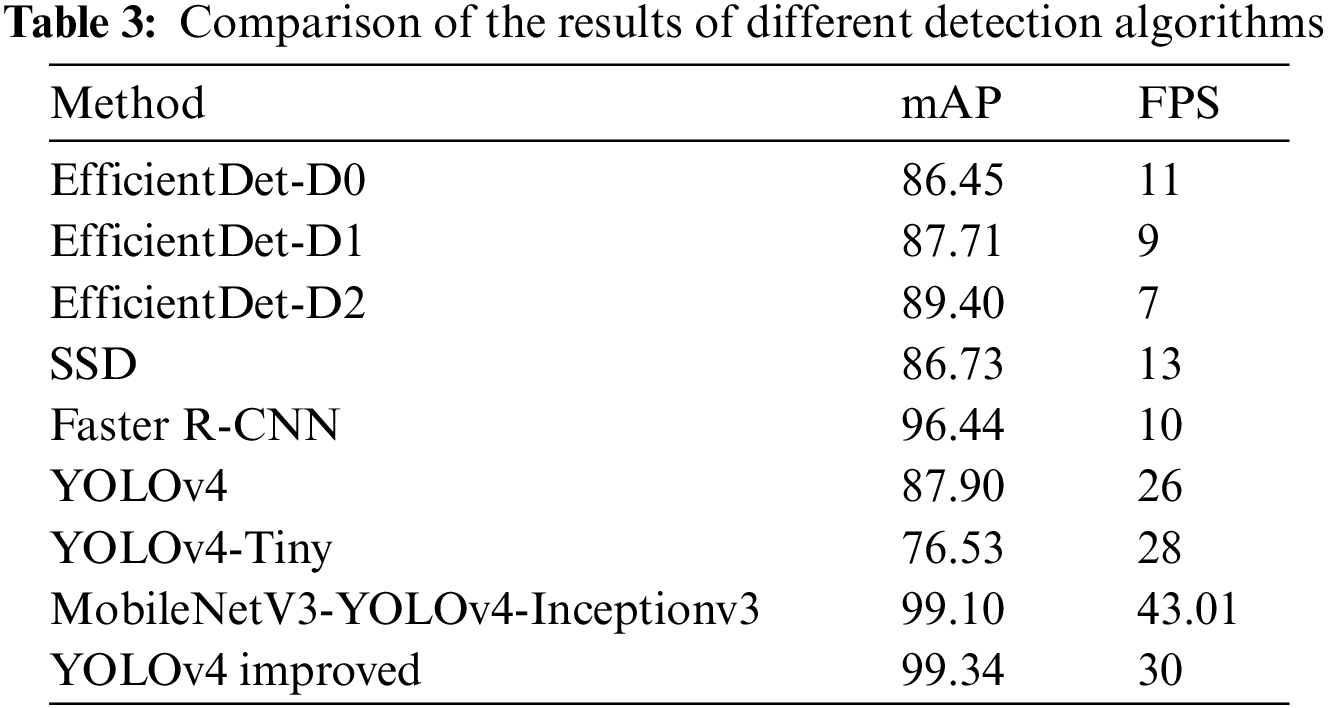
This paper presents numerous good PCB defect detection methods in recent years to compare the performance with the improved network structure in terms of accuracy and speed metrics, as shown in Table 3. Defect detection results are outlined in more detail in the following figures.
The effect of the accuracy curve of the improved algorithm model on the data set through the network improvements and precision clustering performed in this paper is shown in Fig. 3, wherethe horizontal axis indicates the number of training iterations/thousand, and the vertical axis indicates the magnitude of the accuracy rate. In addition, the blue line in Fig. 3a indicates that the accuracy value without precision clustering, while the accuracy value obtained by the precision clustering algorithm used in this paper is about 1.5% higher than it, indicating the importance of the improved algorithm for PCB defect detection in this paper. In addition, the analysis of Fig. 3b shows that the loss function of the PCB defect detection model gradually converges to an approximation of about 0.10, which can be assumed better for practical application detection.
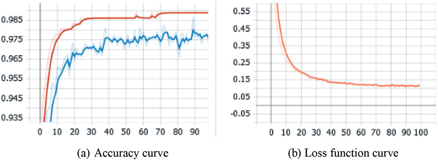
Figure 3: Improved YOLOv4 defect detection effect curve display
In order to further verify the outstanding ability of the defect recognition performance of the algorithm improved by YOLOv4 in this paper, different detection algorithms such as Single Shot Detector (SSD), Faster R-CNN, YOLOv4-Tiny, EfficientDet-D0, EfficientDet-D1, and EfficientDet-D2 are selected for PCB defect data set. SSD can predict class probabilities and bounding boxes of objects based on multi-scale deep features, and can inspect multiple objects at different scale by using its multi-scale configuration [22,23]. The detection performance is compared on the same dataset [24]. Among them, Efficient Det is a target detection algorithm proposed by Google, which uses Efficient Net as the backbone feature extraction network, including eight structures from D0 to D7, and D0, D1, and D2 are used for comparison in this paper. YOLOv4-Tiny is a simplified version of YOLOv4, which uses only two feature layers for classification and regression prediction [25].
As shown in Fig. 4 and Table 3, in terms of detection accuracy, the Mean Average Precision (mAP) values of the improved algorithms proposed in this paper are all higher than other algorithms, 12.61% higher than SSD, 2.9% higher than Faster R-CNN, 12.89% higher than EfficientDet-D0, EfficientDet-D1, and EfficientDet-D2, respectively. 11.63%, and 9.94%, 11.44% are higher than YOLOv4, and 22.81% are higher than YOLOv4-Tiny. In terms of detection speed, this algorithm is faster than EfficientDet-D0, EfficientDet-D1, EfficientDet-D2, and YOLOv4, but lower than YOLOv4-Tiny, MobileNetV3-YOLOv4-Inceptionv3. The main reasons are that YOLOv4-Tiny is a simplified version of YOLOv4 and its number of parameters is much lower than YOLOv4, so it has more advantages in detection speed. Compared with MobileNetV3- YOLOv4-Inceptionv3, the mAP value is 0.24% higher but the detection speed is relatively low. MobileNetv3-YOLOv4-Inceptionv3 introduces Inceptionv3 as the detection network and uses MobileNetV3 as the feature extraction network. In general, the comprehensive comparative analysis of different algorithms can verify the necessity of the modifications made in this paper, and the detection performance of the improved algorithm is better than other algorithms [26].
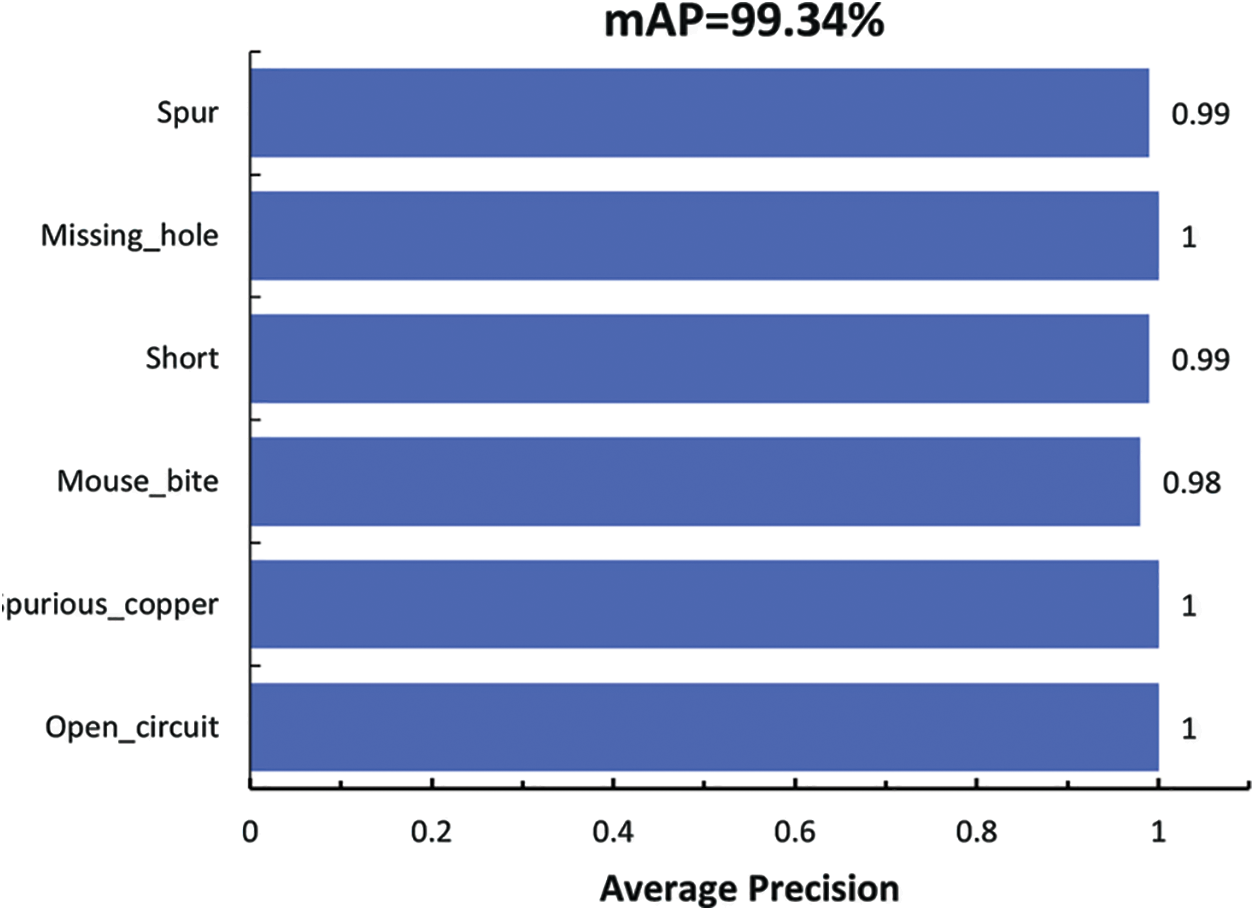
Figure 4: Improved defect detection mAP value display
Overall, the relatively good detection performance results demonstrate the feasibility of the new backbone network structure built by integrating the feature layer with CSPDarknet53, the necessity of the attention mechanism for multi-class feature fusion, and the rationality of obtaining the anchor boxes based on K-means++ clustering.
4.5 Defect Detection Effect Display
The training results of the improved YOLOv4 algorithm proposed in this paper are applied to PCB defect detection, and the detection results are shown in Fig. 5. It can be seen that the method proposed in this paper can accurately achieve the defect detection of PCB. The original YOLOv4 network model is not ideal for defect detection due to its own network problems, as shown in Fig. 5a, and the defect detection process is missing detection phenomenon.
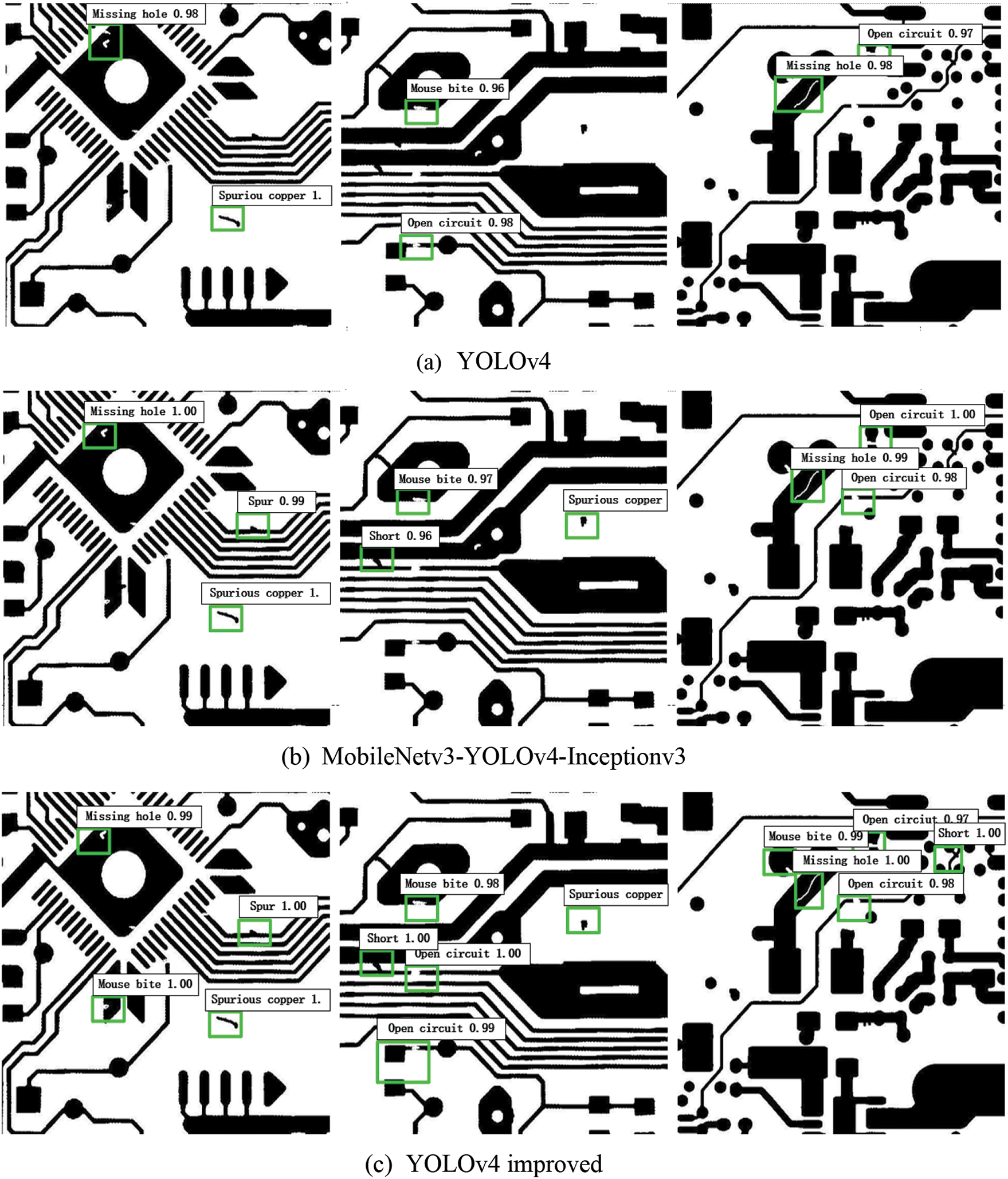
Figure 5: Effect of the defect detection algorithm
However, MobileNetv3-YOLOv4-Inceptionv3 has the problem that the anchor box is not fully used in the output of the feature layer. In this paper, the original CSPDarknet53 backbone network is preserved for PCB defect feature information extraction, and the original multi-layer cascade fusion method is changed to a single-layer feature layer structure to greatly avoid the uneven distribution problem of anchor boxes size during PCB defect detection.
Then the K-means++ clustering method is used for precise clustering of the anchor boxes to obtain the required size requirements for the defect detection, thus further improving the recognition and localization of small PCB defects. As shown in Fig. 5c, the detection effect is relatively obvious.
Because the traditional detection method has the disadvantages of low defect detection efficiency, large defect identification and localization error, and poor versatility of the detection method, this paper is mainly to further improve the recognition performance and localization effect of high-resolution small target PCB defect detection. The paper analyzes the PCB surface defect detection algorithm and proposes a defect detection method based on YOLOv4, which has better detection capability, lower leakage rate and false detection rate. The research work done in this paper can further meet the requirements of high detection accuracy, real-time and interactivity required by PCB industry in real production life. However, some challenges remain to be overcome. When unbalanced data is considered, the model does not perform well enough. Further researches should describe PCB defects in detail and classify defects into predefined categories. Moreover, the fully automatic training without human interference with transfer learning and meta-learning should be developed to improve the accuracy.
Funding Statement: This work was funded by the Natural Science Research Project of Higher Education Institutions in Jiangsu Province (No. 20KJA520007). Min Zhang receives the grant and the URLs to sponsors’ websites are http://jyt.jiangsu.gov.cn/.
Conflicts of Interest: The authors declare that they have no conflicts of interest to report regarding the present study.
References
1. N. Zeng, P. Wu and Z. Wang, “A small-sized object detection oriented multi-scale feature fusion approach with application to defect detection,” IEEE Transactions on Instrumentation and Measurement, vol. 71, pp. 1–14, 2022. [Google Scholar]
2. Y. J. Ren, Y. Leng, J. Qi, K. S. Pradip, J. Wang et al., “Multiple cloud storage mechanism based on blockchain in smart homes,” Future Generation Computer Systems, vol. 115, no. 3, pp. 304–313, 2021. [Google Scholar]
3. M. B. Akhtar, “The use of a convolutional neural network in detecting soldering faults from a printed circuit board assembly,” HighTech and Innovation Journal, vol. 3, no. 1, pp. 1–14, 2022. [Google Scholar]
4. W. Zhao, S. R. Gurudu and S. Taheri, “PCB component detection using computer vision for hardware assurance,” Big Data and Cognitive Computing, vol. 6, no. 2, pp. 39, 2022. [Google Scholar]
5. K. Liu, K. L. Huang, S. Sfarra, J. Yang, Y. Liu et al., “Factor analysis thermography for defect detection of panel paintings,” Quantitative InfraRed Thermography Journal, 2021. https://doi.org/10.1080/17686733.2021.2019658 [Google Scholar] [CrossRef]
6. K. Simmen, B. Buch, A. Breitbarth and G. Notni, “Non-destructive inspection system for MAG welding processes by combining multimodal data,” Quantitative InfraRed Thermography Journal, vol. 18, no. 1, pp. 1–17, 2021. [Google Scholar]
7. Y. J. Ren, F. J. Zhu, S. P. Kumar, T. Wang, J. Wang et al., “Data query mechanism based on hash computing power of blockchain in internet of things,” Sensors, vol. 20, no. 1, pp. 1–22, 2020. [Google Scholar]
8. C. Solorzano and D. M. Tsai, “Environment-adaptable printed-circuit board positioning using deep reinforcement learning,” IEEE Transactions on Components, Packaging and Manufacturing Technology, vol. 12, no. 2, pp. 382–390, 2022. [Google Scholar]
9. R. Parvathi, A. S. Janardhan and S. Meenakshi, “Printed circuit board defects detection based on oriented fast and rotational brief with super resolution,” International Journal of Progressive Research in Science and Engineering, vol. 3, no. 4, pp. 144–151, 2022. [Google Scholar]
10. Y. J. Ren, Y. Leng, Y. P. Cheng and J. Wang, “Secure data storage based on blockchain and coding in edge computing,” Mathematical Biosciences and Engineering, vol. 16, no. 4, pp. 1874–1892, 2019. [Google Scholar] [PubMed]
11. M. Jeon, S. Yoo and S. W. Kim, “A contactless PCBA defect detection method: Convolutional neural networks with thermographic images,” IEEE Transactions on Components, Packaging and Manufacturing Technology, vol. 12, no. 3, pp. 489–501, 2022. [Google Scholar]
12. P. Hurtik, V. Molek and J. Hula, “Poly-YOLO: Higher speed, more precise detection and instance segmentation for YOLOv3,” Neural Computing and Applications, vol. 34, no. 10, pp. 8275–8290, 2022. [Google Scholar]
13. M. Qi, Y. Wang and Y. Chen, “Center detection algorithm for printed circuit board circular marks based on image space and parameter space,” Journal of Electronic Imaging, vol. 32, no. 1, pp. 011002, 2022. [Google Scholar]
14. Y. J. Ren, J. Qi, Y. P. Liu, J. Wang and G. Kim, “Integrity verification mechanism of sensor data based on bilinear map accumulator,” ACM Transactions on Internet Technology, vol. 21, no. 1, pp. 1–20, 2021. [Google Scholar]
15. X. Zhang and G. Wang, “Stud pose detection based on photometric stereo and lightweight YOLOv4,” Journal of Artificial Intelligence and Technology, vol. 2, no. 1, pp. 32–37, 2022. [Google Scholar]
16. X. Liu, Y. He and H. Huang, “Design and optimization methods of the header of HDI PCB rogowski current sensors,” IEEE Transactions on Instrumentation and Measurement, vol. 71, pp. 1–10, 2022. [Google Scholar]
17. Y. J. Ren, F. Zhu, J. Wang, P. Sharma and U. Ghosh, “Novel vote scheme for decision-making feedback based on blockchain in internet of vehicles,” IEEE Transactions on Intelligent Transportation Systems, vol. 23, no. 2, pp. 1639–1648, 2022. [Google Scholar]
18. R. Ding, L. Dai and G. Li, “TDD-net: A tiny defect detection network for printed circuit boards,” CAAI Transactions on Intelligence Technology, vol. 4, no. 2, pp. 110–116, 2019. [Google Scholar]
19. J. Wang, C. Ju, Y. Gao, A. K. Sangaiah and G. J. Kim, “A PSO based energy efficient coverage control algorithm for wireless sensor networks,” Computers, Materials & Continua, vol. 56, no. 3, pp. 433–446, 2018. [Google Scholar]
20. S. Tang, F. He and X. Huang, “Online PCB defect detector on a new PCB defect dataset,” 2019. [Online]. Available: https://doi.org/10.48550/arXiv.1902.06197 [Google Scholar] [CrossRef]
21. Y. Ren, X. Liu, Q. Wu, L. Wang and W. Zhang, “Cryptographic accumulator and its application: A survey,” Security and Communication Networks, vol. 2022, no. 1, pp. 1–13, 2022. [Google Scholar]
22. S. D. Khan, H. Ullah, M. Ullah, N. Conci, F. A. Cheikh et al., “Person head detection based deep model for people counting in sports videos,” in 16th IEEE Int. Conf. on Advanced Video and Signal Based Surveillance, Taipei, Taiwan, 2019. [Google Scholar]
23. S. D. Khan and S. Basalamah, “Scale and density invariant head detection deep model for crowd counting in pedestrian crowds,” Visual Computer, vol. 37, no. 8, pp. 2127–2137, 2021. [Google Scholar]
24. V. A. Adibhatla, H. C. Chih and C. C. Hsu, “Defect detection in printed circuit boards using you-only-look-once convolutional neural networks,” Electronics, vol. 9, no. 9, pp. 1547–1564, 2020. [Google Scholar]
25. M. Li, N. Yao and S. Liu, “Multisensor image fusion for automated detection of defects in printed circuit boards,” IEEE Sensors Journal, vol. 21, no. 20, pp. 23390–23399, 2021. [Google Scholar]
26. Q. Wu, Z. Han, G. Mohiuddin and Y. Ren, “Distributed timestamp mechanism based on verifiable delay functions,” Computer Systems Science & Engineering, vol. 44, no. 2, pp. 1633–1646, 2023. [Google Scholar]
Cite This Article
 Copyright © 2023 The Author(s). Published by Tech Science Press.
This work is licensed under a Creative Commons Attribution 4.0 International License , which permits unrestricted use, distribution, and reproduction in any medium, provided the original work is properly cited.
 Downloads
 Citation Tools