
 Submit a Paper
 Propose a Special lssue
 Open Access
ARTICLE

High Efficient Reconfigurable and Self Testable Architecture for Sensor Node
1
Department of Electronics and Instrumentation Engineering, Meenakshi College of Engineering, Chennai, India
2
Department of Electronics and Communication Engineering, CEG Campus, Anna University, Chennai, India
* Corresponding Author: G. Venkatesan. Email:
Computer Systems Science and Engineering 2023, 46(3), 3979-3991. https://doi.org/10.32604/csse.2023.031627
Received 22 April 2022; Accepted 27 June 2022; Issue published 03 April 2023
 View Full Text
 Download PDF
Abstract
Sensor networks are regularly sent to monitor certain physical properties that run in length from divisions of a second to many months or indeed several years. Nodes must advance their energy use for expanding network lifetime. The fault detection of the network node is very significant for guaranteeing the correctness of monitoring results. Due to different network resource constraints and malicious attacks, security assurance in wireless sensor networks has been a difficult task. The implementation of these features requires larger space due to distributed module. This research work proposes new sensor node architecture integrated with a self-testing core and cryptoprocessor to provide fault-free operation and secured data transmission. The proposed node architecture was designed using Verilog programming and implemented using the Xilinx ISE tool in the Spartan 3E environment. The proposed system supports the real-time application in the range of 33 nanoseconds. The obtained results have been compared with the existing Microcontroller-based system. The power consumption of the proposed system consumes only 3.9 mW, and it is only 24% percentage of AT mega-based node architecture.Keywords
Like numerous key advancements, Wireless Sensor Networks (WSN) began from military applications, for example, the systems of acoustic sensors previously conveyed during the 1950 s for submarines [1]. In the 1980 s, the United States defense advanced research projects agency concentrated its exploration on computation, distributed sensing, and communication within the Distributed Sensor Networks (DSN) [2]. In the 1990 s, the advancements in wireless communication technologies enabled actual WSNs from wired DSNs [3,4]. This opened the WSN innovation to a wide range of nonmilitary personnel applications, for example, checking ecological boundaries and modern procedures, the following objects, and identifying events [5].
These days, the exploration endeavors on WSNs are converged with embedded frameworks and the arrangement of framework planning techniques, yielding Cyber Physical Systems (CPS) [6]. Many Internet of Things (IoT) solutions are provided in WSNs [7,8]. CPS is focused on serving a variety of applications, and is not restricted to specific nodes. CPS nodes get connected to open communication networks, thus causing significant development of the IoT [7]. For a few applications like home automation and smart home appliances, which require less data rate, IEEE [802.15.4]-based protocol suffices. Often, WSNs are small tiny units connected with several sensor nodes with a specific network topology. Intermediate nodes also contribute to the data transmission from one end to the other [9] with applications in critical areas like monitoring environmental threats and disaster management [10]. It is essential to secure the nodes as they may be damaged by harsh weather conditions which may sometimes cause the whole system to fail. Along these lines, the fault detection of the node network is significant for guaranteeing the exactness of checking results.
A robust security protocol for communicating through WSN is mandatory if it has to be used in some mission-critical tasks. However, providing satisfactory security protection in WSNs has been challenging due to various network and resource constraints and malicious attacks. Hence specific Integrated circuits, Application Specific Integrated Circuits (ASIC) can work efficiently managing data security and accelerate computation and data transfer [11,12]. Because of their absence of adaptability and high Non Recurring Engineering (NRE) costs, ASIC is not a feasible choice for the research model and is subsequently not looked into in more detail. Programmable integrated circuits such as a Field Programmable Gate Array (FPGA) would be a good choice considering the massively parallel hardware available and low NRE cost compared to ASIC. Hence our research work proposes wireless sensor node architecture integrated with a self-testing core and cryptoprocessor to provide fault-free operation along with secured data transmission. To solve the power consumption and increase the speed of the operation, this research work proposes the sensor node architecture, which is designed in FPGA with reconfigurable selection.
This paper is organized in such a way that Section 1 gives the introduction to the node architecture. Related works are discussed in Section 3. The proposed secured and self-testable wireless sensor node architecture has been explained in this Section 4. Results of the proposed research work have been discussed and analyzed in Section 5. The conclusion of the proposed sensor node architecture has been explained in this Section 6.
A sensor network comprises various little embedded designs (named sensor nodes), which convey remotely to resolve a joint task. They are commonly utilized as effectively deployable information acquisition systems to screen the transient and spatial qualities of surrounding physical quantities, for example, Temperature, Pressure, Flow, Humidity, Structural vibration, etc. Fig. 1 shows the sample monitoring application of WSN in the dedicated gateway node all the information accumulated by the WSN has to be collected.

Figure 1: Example WSN monitoring application, which scents the collected data from the end (leaf) nodes to intermediates routers and a committed gateway to an isolated base station
The collected information in the gateway is stored steadily or sent to a remote base station through a wide area network such as a mobile cellular radio link. Along with the signal monitoring, the Nodes are used to track the objects or the signal collecting nodes may be attached to a WSN application [11]. Likewise, the necessities and capacities of the nodes shift emphatically between various applications, and even inside a specific network, the architecture of ordinary WSN nodes comprises the five conventional units shown in Fig. 2. Digital or analog sensors catch the pertinent signals at fixed intervals ranging from a few seconds in ecological monitoring [13] down to a few milliseconds in vibration-based secondary health checking [14] or even beneath in acoustic restriction applications [15]. Before processing or transmission sampled data should be stored in the memory module.

Figure 2: Generic architecture of a sensor node
Normally the internal memory of any processor is limited to a few kilobytes. This internal memory is not enough to store long-duration sampled data. So, Flash Programmable Random Access Memory (FRAM) or Flash memory should be attached with the WSN nodes [16–18]. The main part of the node is a processor that controls or coordinates the memory, transceiver, and sensors. Most of the simple nodes are designed based on Atmel or the 16 bit Texas Instrument controller. More sophisticated nodes are designed using the advanced reduced instruction set computer machine microcontrollers or power full digital signal processors [19].
Apart from the regular processor, the integration of ASICs of proposed by some of the WSN projects [20,21]. Security is essential for the application, for example, battlefield, environmental observation, and smart home to be executed. To ensure the data security of WSN, it is important to recognize nodes [21–22]. In any case, it is a test for the nodes to run encryption calculations and store information because of the restricted computational capacity and resources. Compare to the Rivest–Shamir–Adleman (RSA), Advanced Encryption Standards (AES) takes lesser time and gives better security than Secure Hash Algorithms (SHA) [20]. To reduce the power consumption altering the data path is suggested several multipliers reduced in [22]. To prove the hardware efficiency the architecture can be implemented in a field-programmable gate array [23]. In [24], a novel FPGA implementation of a new AES architecture is analyzed and compared with the different AES implementations and proved that the new architecture has high speed and reduced area. To guarantee a long-term activity without the power supply in an environment, a nonconventional power supply gracefully has been chosen and a low power utilization structure of a water level observing station was proposed in [25]. A low-power WSN for smart grid application along with cyber security is presented in [26] can sense and separate various attacks in a well-organized manner.
3 Proposed Secured and Self Testable Wireless Sensor Node Architecture
The proposed wireless sensor node architecture performs three major functions such as self testable, automatic or manual transmission, secured or unsecured transmission. All three functions have been implemented by three major hardware units.
1. Testing core responsible for testing the node whenever initializing the node.
2. A regular processor is used to perform the computation and transmission with manual and automatic modes.
3. A cryptoprocessor for transmitting the collected data a secured manner.
High-speed low area AES architecture has been proposed for secured transmission. All three operations are controlled by a state machine which depends on the inputs from sensor node architecture. Fig. 3 shows the proposed sensor node architecture. The input pins are automatic/manual, secured or unsecured, clock, reset, data input from Analog to Digital Converter (ADC). The output pins are data out which enable and ensure the transmitted data is collected from one of the sensors from the group of eight sensors. Tx completed pin indicates the completion of Transmission. Three-bit ADC selection pin selects the ADC input to convert the analog to digital data from any one of the inputs. An output pin ADC pin enables the ADC for the conversion. The detailed block diagram of the proposed node architecture is given in Fig. 4.

Figure 3: Proposed secured and self testable wireless sensor node architecture
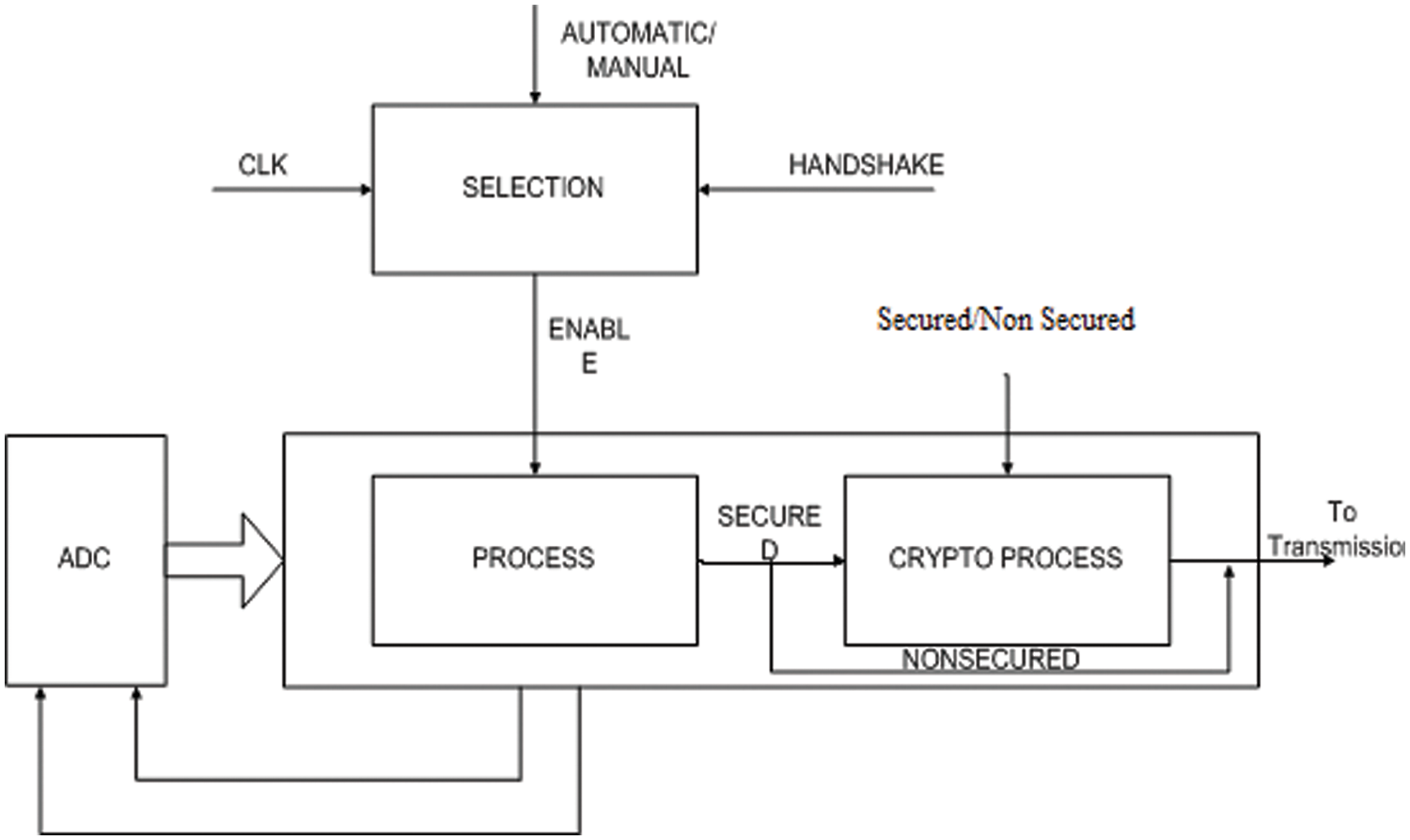
Figure 4: Block diagram of proposed sensor node architecture
The main function of node architecture is collecting the data from various sensors through the ADC unit and computing the required format. The computed data is encrypted using a crypto processor and includes the error-correcting codes before transmitting. The entire control signal required for the remaining units is issued by the data process unit only. So the major part of the work of wireless sensor node architecture is carried out by the data processor unit only. The major unit of data process is sensor subsystem, controlling of ADC unit and process of collecting data. The function of the data process unit is explained through the state machine and flow charts given in the following sections.
Data process unit comprises the physical sensors and ADC. It acts as the interface between the physical environment and virtual world, i.e., collecting data from the environment and converting this data from analog to digital signal for smooth processing.
a. Sensor: A sensor senses physical parameters such as temperature, flow, pressure, level, motion, speed, etc, and convert them into electrical (analog) signal. A WSN incorporates countless sensor nodes with every node containing at least one sensor relying upon the application territory. There is a range of sensor types that can be employed in WSNs. An example of sensor classification is active and passive sensors. Active sensors do not need any external power supply for conversion of physical quantity into electrical quantity examples for active transducers/sensors are thermocouple and piezoelectric transducer. Alternatively, passive sensors require an external power supply to convert physical quantity into electrical quantity. Resistance thermometers, linear variable differential transformer, strain gauges are good examples of passive sensors.
b. Analog-to-Digital Converter (ADC): The output of a sensor is an analog signal. This means there needs to be an interface between the sensor and the digital processor (microcontroller). The ADC converts the output of a sensor which is a continuous, analog signal into a digital signal [1].
Fig. 5 shows the state machine of the proposed sensor node architecture.
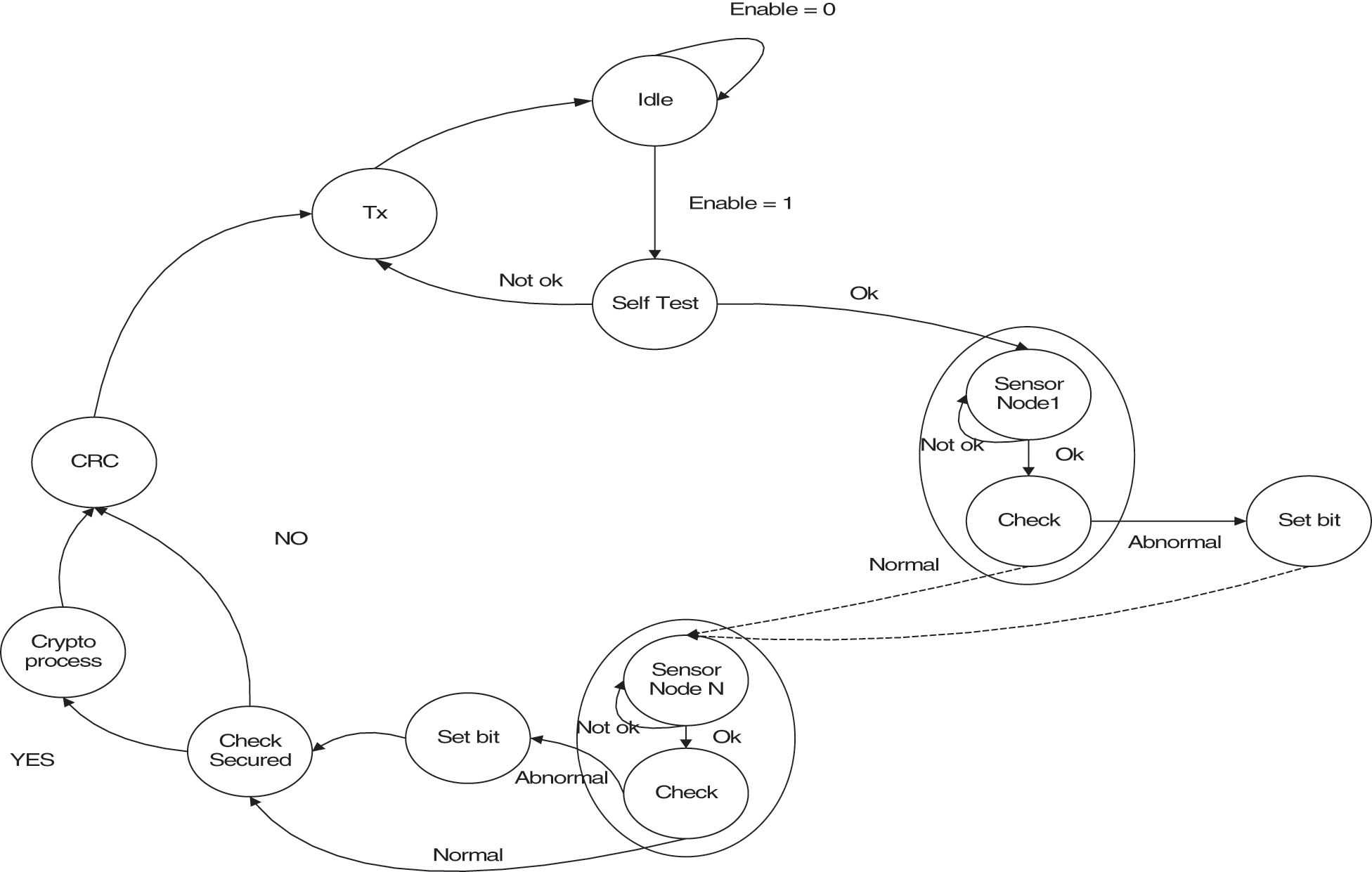
Figure 5: The state machine of the proposed sensor node architecture
During testing mode, the processor selects one channel out of 8 input channels. And the ADC is connected first with a maximum reference voltage and the converted digital signal is verified with register. Second, the input is connected with 50% of a reference voltage and the converted digital equivalent is compared with stored value if it is within the tolerance it goes to test the next input value otherwise sets the bit as a fault, and information is passed as the specific channel failed. If the 50% conversion voltage is correct then the next input to the channel is ground and compare the converted result with the tolerance level for setting the channel is a defect or not. Similarly, all the channels are tested for three cases and then the fault field in the packet is set as a logical one. After satisfying the operation of the ADC the self-test verifies the cryptoprocessor if the architecture is selected as secured otherwise the processor continues the regular operation. The cryptoprocessor is tested by sending a predefined input and verifying the output with stored results if the output of the cryptoprocessor is the same as the stored results then the fault field in the packet is cleared otherwise it is set as a logical one. The processing is explained in Fig. 6. The tolerance is set as the given equation
where Ya is the stored result and Yb is the output of cryptoprocessor
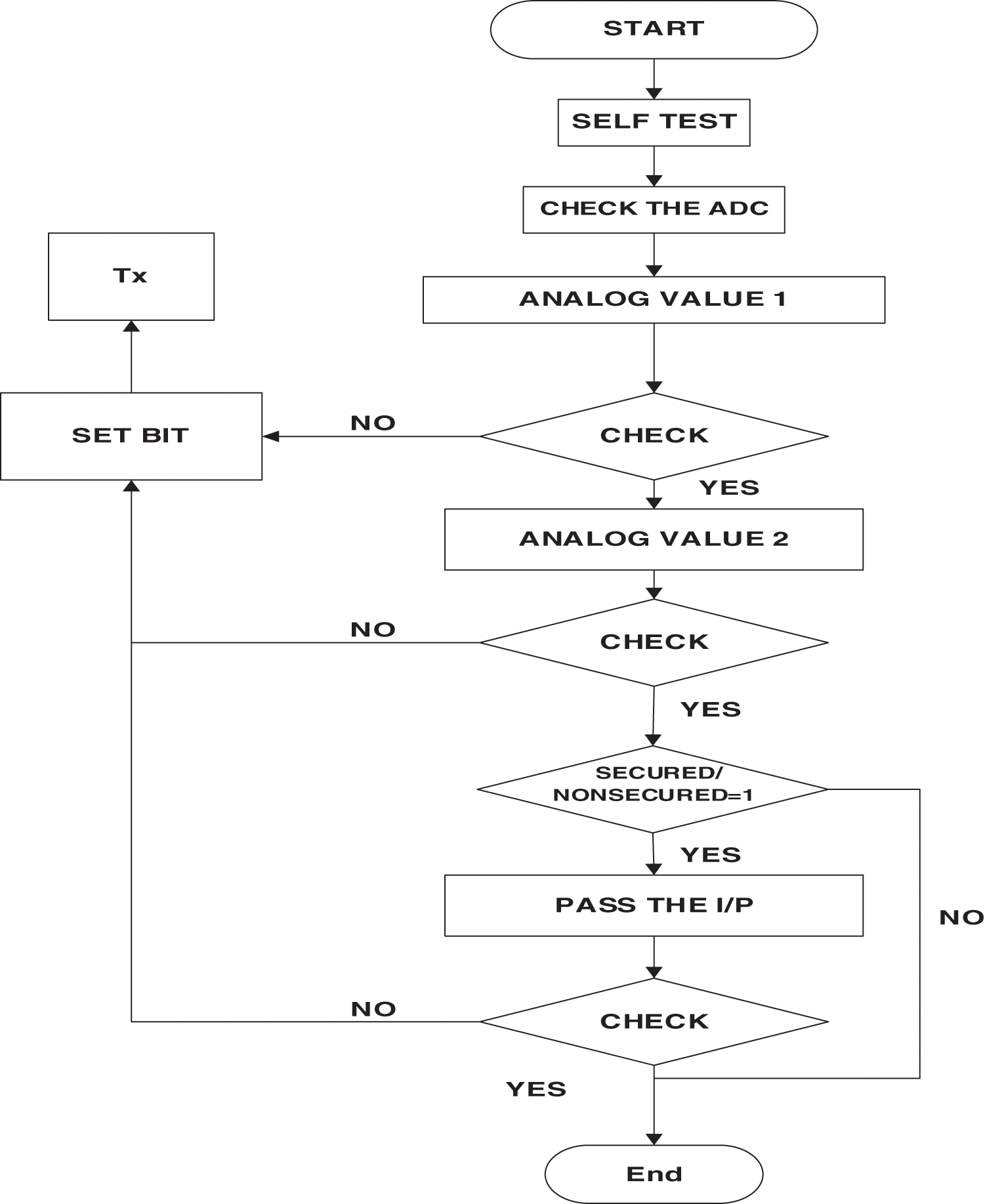
Figure 6: Flow chart of Sensor node architecture
The AES can be customized in programming or worked with unadulterated equipment. Anyway, FPGAs offer a snappier, more adaptable arrangement. This research proposes a crypto processor using the AES algorithm concerning FPGA and the Verilog. In this research, a high-performance AES architecture implementation with MUX-based substitution box (S-Box) and random round selection is proposed. The byte substitution process implemented by S-Box is a significant part of the AES. In the novel FPGA implementation, a new AES architecture has been analyzed and compared in terms of area, speed and power with the different AES implementations. This crypto processor consists of 20-pins as well as works with 3.3 V power supply. This processor can be work at a 100 MHz of maximum frequency.
The 10-byte packet format for the self-testable unit is arranged in little-endian mode. The byte 0, 1, 2, 3 5, 6, 7, 8 are assigned to ADC output channel 0 to 7 respectively. The ADC accept maximum of eight channels. The 4th byte is reserved for user operation. The 9th byte contains the control and status bits. The 7th bit of 9th byte is used for testing result up dation. The bit is set as the node fails during the testing operation otherwise fault free. The 6th bit indicates that the sensor value is normal or abnormal. This bit is set when any channel output is abnormal. The 5th bit is used to indicate the processor is in secured or unsecured mode. Fig. 7 shows the Packet format used in the proposed node architecture.
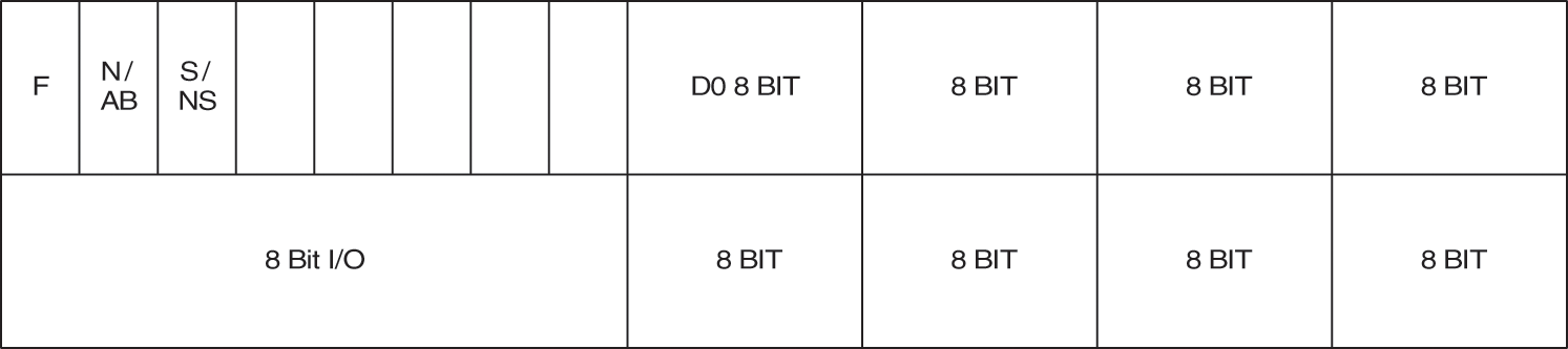
Figure 7: The packet format for the proposed wireless sensor node architecture
3.4 Error Correction Code (ECC)
To improve the reliability of remote transmission, an Error Correction Code (ECC) was included in the proposed testable WSN. After the EEC scrambled the signs, the ECC includes extra bits called redundancy codes before the transmission of information. The beneficiary can check whether transmission information is right or with blunder before decoding the information received. By creating a polynomial function, the ECC procedure can diminish transmission blunder.
All the three modules in the proposed architecture have been designed and implemented using Verilog programming. These three basic units are controlled by state machines and it has also been designed using Verilog programming. Individual units are simulated with the help of the ModelSim SE 6.5b version simulator. The mealy model is used to design the state machine. There are 12 states in the design to control the operation of node architecture. The entire architecture has been synthesized using the Xilinx EDA tool for hardware implementation. Table 1 shows the device utilization summary and power consumption of the proposed sensor node architecture for the target of Spartan 3E FPGA. Fig. 8 shows the simulation result of node architecture.
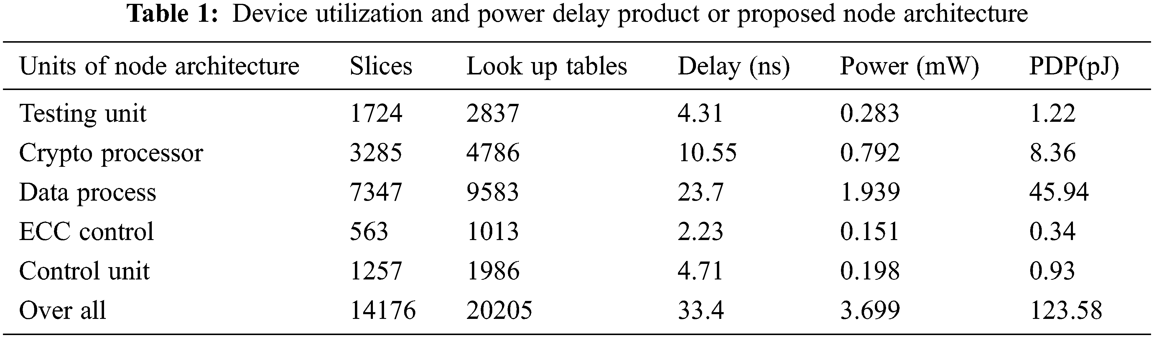
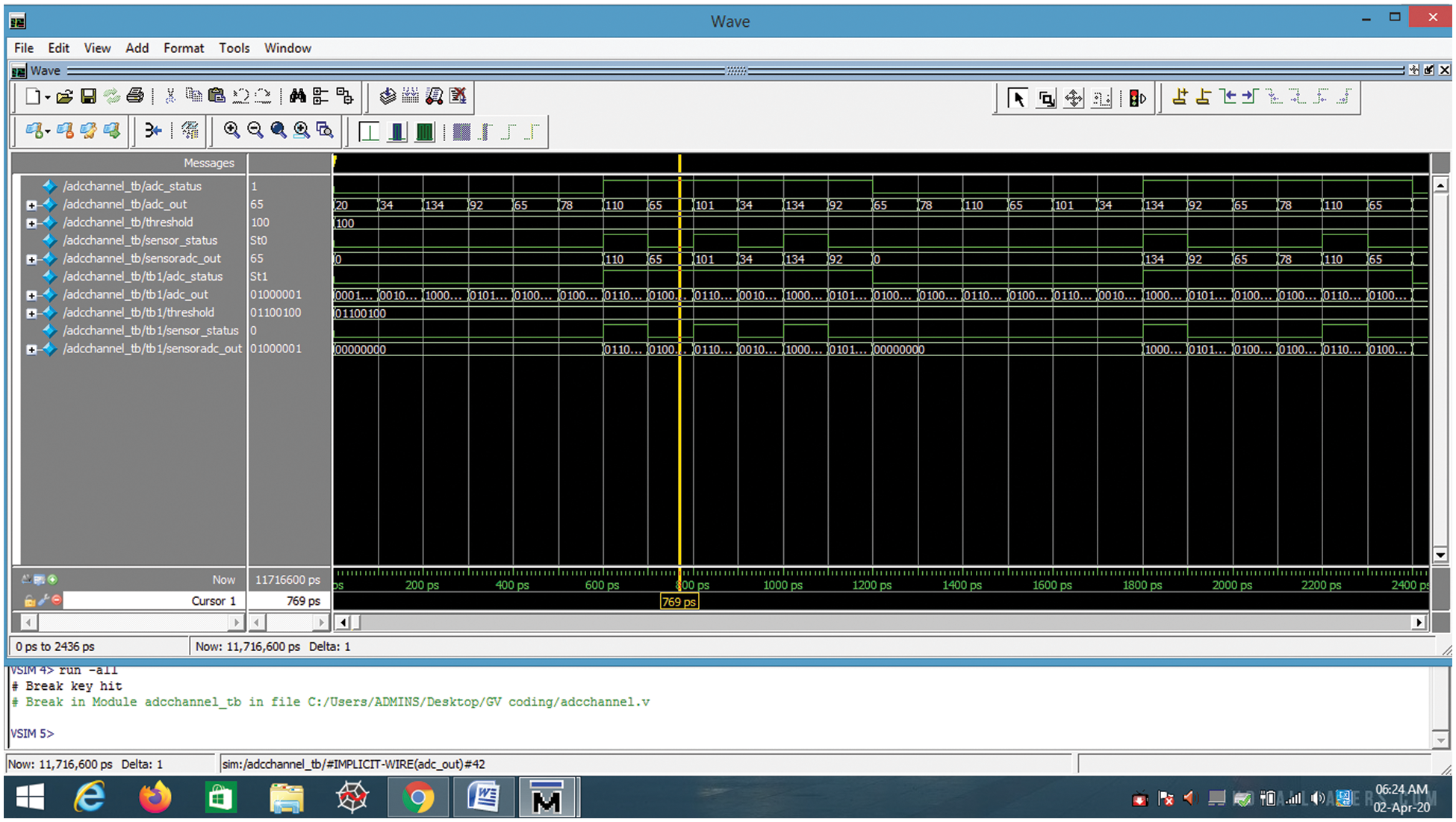
Figure 8: Simulation result node architecture
From Table 1 the data process unit consumes 7347 slices out of 14176 slices consumed by the overall units. Except the Crypto processor the proposed featured processor increases 6829 slices. At the cost of area increased, the proposed system offers addition features such as self testing, error correction and Crypto processing. This has been a major area of overall node architecture. Fig. 9 shows the device utilization summary of node architecture. From Fig. 9, the area is utilized by the various units such as testing unit, cryptoprocessor, Data processor, ECC unit, and control units.
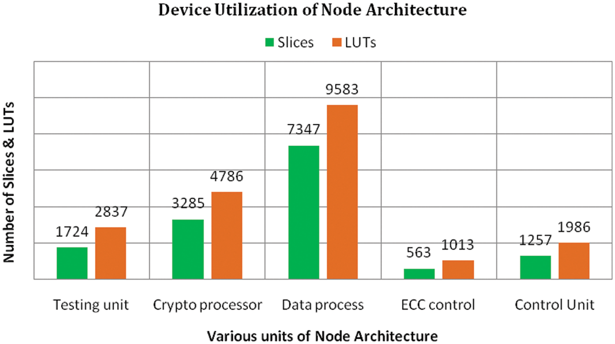
Figure 9: Device utilization summary of various units of node architecture
The percentage of area occupied by the various units is shown in Fig. 10. From the Fig. 10, the data process unit consumes 52%. The remaining units such as testing and cryptoprocessor are the additional units apart from the basic unit and also these units consume only less area compared with the data process unit. It is 12% and 23% respectively. From the Look Up Table (LUT) utilization chart, the data process unit consumes 47% and the testing, crypto processors consume 14% and 24% respectively.

Figure 10: Percentage of device resources used by various units of node architecture. (a) Area in terms of number of slices (b) Area in terms of LUT
Fig. 11 shows the propagation delay of different units of the proposed node architecture. The data process unit of node architecture is the major essential unit of node architecture and also it takes a longer propagation delay of overall node architecture. Its takes 23.7 ns, the frequency (T) of operation of this data process unit is 42.19 MHz. Next to the data process, the cryptoprocessor takes a propagation delay of 0.55 ns. The remaining units will be operated with a higher frequency than the data process and cryptoprocessor.
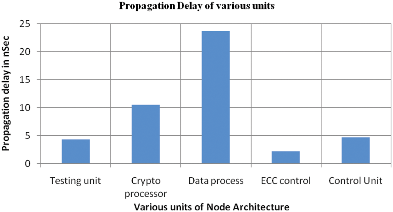
Figure 11: Propagation delay of various units of node architecture
Fig. 12 shows the power consumed by the various units of the proposed node architecture. Out of all units, the data processor unit consumes 1.939 mW. This power consumption is 51 percent of the power consumption of overall units of node architecture. The major operation of node architecture is handled by the data processor, It controls the ADC operation as well as collecting the data from all sensors and converting them to ciphertext if the security is included. Otherwise, the collected data is added with ECC and converted to packet format before transmission. To test the node architecture the proposed testing unit takes 4.3 nanoseconds.

Figure 12: Power consumed by various units of node architecture
Fig. 13 shows the Power Delay Product (PDP) of node architecture in terms of various parts power delay product. From the chart, the ECC unit power delay product is very negligible compared with the data process unit. Even though the ECC unit consumes a considerable area, the power delay product is very less. The area consumed by the cryptoprocessor is 24% but the power delay product is only 8.36 pJ. It is only 18% of the data process unit.
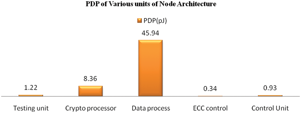
Figure 13: PDP of various units in proposed node architecture
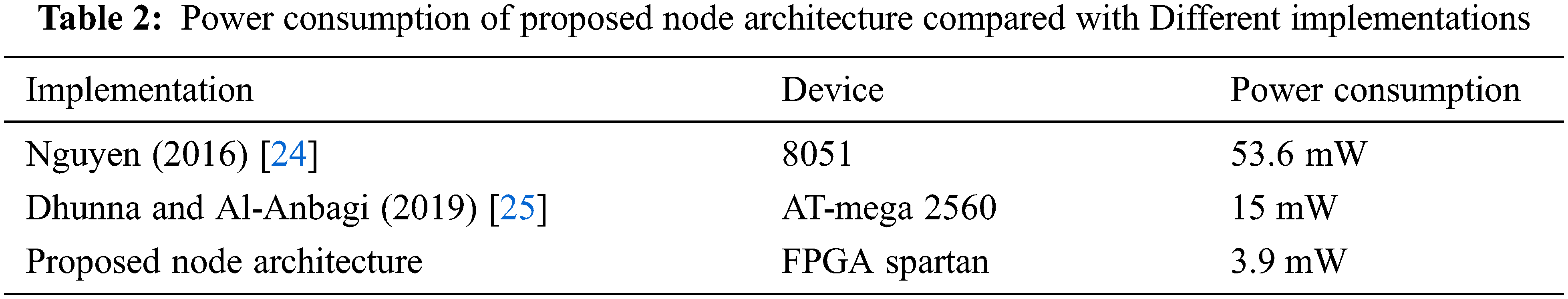
Table 2 shows the comparison of power consumed by the proposed method and various microprocessor implementations. From Table 2, it is clear that the proposed work consumes only 3.9 mW compared with the 8051 microcontroller-based node architecture consumes 53.6 mW [24] and ATmega 2560 based architecture consumes 15 mW power [25].
Sensor Network is a significant segment of present-day mobile communication systems. However, node execution is genuinely influenced because of the process unit failures. Therefore, a low-power consumption fault detection method in WSNs has been proposed in this work. The testing mechanism consumes only 2.7% of the data process unit. Similarly, next to the data process unit, the crypto process consumes 50% of the area of the data process unit. The power delay product of this unit is 18% of the data process unit. All other units of the proposed node architecture consume only 25% PDP of main processing. The power consumption of the proposed WSN architecture is 24% of the wireless sensor node architecture implemented by Dhuna using an Atmega processor. The frequency of operation of the proposed system is 29.94 MHz and the system supports the real-time application in the range of 33 nanoseconds. The advantage of the proposed sensor network architecture is programmable with security and testing units.
Funding Statement: The authors received no specific funding for this study.
Conflicts of Interest: The authors declare that they have no conflicts of interest to report regarding the present study.
References
1. H. Silverstein, “CEASAR, SOSUS, and submarines: Economic and institutional implications of ASW technologies,” OCEANS, Washington, DC, USA, pp. 406–410, 1978. [Google Scholar]
2. S. Kumar and D. Shepherd, “SensIT: Sensor information technology for the warfighter,” in Proc. of the 4th Int. Conf. on Information Fusion, Sun City, South Africa, pp. 1–7, 2001. [Google Scholar]
3. G. Asada, M. Dong, T. S. Lin, F. Newberg, G. Pottie et al., “Wireless integrated network sensors: Low power systemson a chip,” in Solid-State Circuits Conf., ESSCIRC ‘98, Proc. of the 24th European, Hague, the Netherlands, pp. 9–16, 1998. [Google Scholar]
4. C. Y. Chong and S. P. Kumar, “Sensor networks: Evolution, opportunities, and challenges,” in Proc. of the IEEE, Torino, Italy, vol. 91, no. 8, pp. 1247–1256, 2003. [Google Scholar]
5. P. J. Mosterman and J. Zander, “Cyber-physical systems challenges: A needs analysis for collaborating embedded software systems,” Software & Systems Modeling, vol. 15, pp. 1–12, 2015. [Google Scholar]
6. L. Mainetti, L. Patrono and A. Vilei, “Evolution of wireless sensor networks towards the internet of things: A survey,” in Int. Conf. on Software, Telecommunications and Computer Networks, Split Croatia, pp. 1–6, 2011. [Google Scholar]
7. Z. Chen, M. He, W. Liang and K. Chen, “Trust-aware and low energy consumption security topology protocol of wireless sensor network,” Journal of Sensors, vol. 2015, pp. 1–10, 2015. [Google Scholar]
8. S. Sánchez-Solano, E. Camacho-Ruiz, M. C. Martínez-Rodríguez and P. Brox, “Multi-unit serial polynomial multiplier to accelerate NTRU-based cryptographic schemes in IoT embedded systems,” Sensors, vol. 22, no. 5, pp. 1–27, 2022. [Google Scholar]
9. M. P. Fanti, A. M. Mangini and W. Ukovich, “Fault detection by labeled petri nets in centralized and distributed approaches,” IEEE Transactions on Automation Science and Engineering, vol. 10, no. 2, pp. 392–404, 2013. [Google Scholar]
10. P. Rawat, K. D. Singh, H. Chaouchi and J. M. Bonnin, “Wireless sensor networks: A survey on recent developments and potential synergies,” The Journal of Supercomputing, vol. 68, no. 1, pp. 1–48, 2014. [Google Scholar]
11. M. T. Lazarescu, “Design of a WSN platform for long-term environmental monitoring for IoT applications,” IEEE Journal on Emerging and Selected Topics in Circuits and Systems, vol. 3, no. 1, pp. 45–54, 2013. [Google Scholar]
12. Y. Lu, J. Zhai, R. Zhu and J. Qin, “Study of wireless authentication center with mixed encryption in WSN,” Journal of Sensor, vol. 2016, pp. 1–8, 2016. [Google Scholar]
13. N. de Battista, J. M. Brownjohn, J. A. Rice, S. H. Sim and H. P. Tan, “Wireless structural monitoring of a multi-span footbridge with decentralised embedded data processing,” in Int. Conf. on Structural Health Monitoring of Intelligent Infrastructure, Rome, pp. 1–10, 2013. [Google Scholar]
14. S. Astapov, J. Ehala and J. S. Preden, “Collective acoustic localization in a network of dual channel low power devices,” in Int. Conf. on Mixed Design of Integrated Circuits Systems, Lublin, Poland, pp. 430–435, 2014. [Google Scholar]
15. Y. Jennifer, B. Mukherjee and D. Ghosal, “Wireless sensor network survey,” The International Journal of Computer and Telecommunications Networking, vol. 52, pp. 2292–2330, 2008. [Google Scholar]
16. Y. Zhao, J. R. Smith and A. Sample, “NFC-WISP: A sensing and computationally enhanced near-field RFID platform,” in IEEE Int. Conf. on RFID, Las Vegas, pp. 174–181, 2015. [Google Scholar]
17. A. Ravinagarajan, D. Dondi and T. S. Rosing, “DVFS based task scheduling in a harvesting WSN for structural health monitoring,” in Design, Automation & Test in Europe Conf. & Exhibition, Dreston, pp. 1518–1523, 2010. [Google Scholar]
18. J. Wang, Y. Gao, C. Zhou, S. Sherratt and L. Wang, “Optimal coverage multi-path scheduling scheme with multiple mobile sinks for WSNs,” Computers, Materials & Continua, vol. 62, no. 2, pp. 695–711, 2020. [Google Scholar]
19. K. Shahzad, “Energy efficient wireless sensor node architecture for data and computation intensive applications,” Ph.D. dissertation, Mid Sweden University, Sweden, 2014. [Google Scholar]
20. C. Walravens and W. Dehaene, “Low-power digital signal processor architecture for wireless sensor nodes,” IEEE Transactions on Very Large Scale Integration Systems, vol. 22, no. 2, pp. 313–321, 2014. [Google Scholar]
21. D. Vaithiyanathan, R. Seshasayanan, S. Anith and K. Kunaraj, “A Low-complexity DCT approximation for image compression with 14 additions only,” in Int. Conf. on Green Computing, Communication and Conservation of Energy, Chennai, India, pp. 303–307, 2013. [Google Scholar]
22. K. K. Senthilkumar, K. Kunaraj and R. Seshasayanan, “Implementation of computation-reduced DCT using a novel method,” EURASIP Journal on Image and Video Processing, vol. 2015, no. 1, pp. 1–8, 2015. [Google Scholar]
23. G. Venkatesan and J. R. Perinbam, “A new reconfigurable hardware architecture for cryptography applications using AES by different substitution box(S-box) and random round selection,” International Journal of Computer Science and Network Security, vol. 11, no. 12, pp. 112–116, 2011. [Google Scholar]
24. T. Nguyen, “Energy efficient wireless sensor network and low power consumption station design for an urban water level monitoring system,” in National Foundation for Science and Technology Development Conf. on Information and Computer Science, Danang, pp. 252–256, 2016. [Google Scholar]
25. G. S. Dhunna and I. Al-Anbagi, “A low power WSNs attack detection and isolation mechanism for critical smart grid applications,” IEEE Sensors Journal, vol. 19, no. 13, pp. 5315–5324, 2019. [Google Scholar]
26. W. Kim, M. M. Umar, S. Khan and M. A. Khan, “Novel scoring for energy-efficient routing in multi-sensored networks,” Sensors, vol. 22, no. 4, pp. 1–21, 2022. [Google Scholar]
Cite This Article
 Copyright © 2023 The Author(s). Published by Tech Science Press.
This work is licensed under a Creative Commons Attribution 4.0 International License , which permits unrestricted use, distribution, and reproduction in any medium, provided the original work is properly cited.
 Downloads
 Citation Tools