
 Submit a Paper
 Propose a Special lssue
 Open Access
ARTICLE

Investigations on the Optimization of Contacts Barrier Height for the Improved Performance of ZnO/CdS/CZTS Solar Cells
1 Material Science and Informatics Laboratory, University of Djelfa, Djelfa, 17000, Algeria
2 Faculty of Sciences, University of M’sila, M’sila, 28000, Algeria
3 Department of Physics, University of Constantine, Constantine, 25000, Algeria
4 Department of Physics, Division of Science and Technology, University of Education, Lahore, Pakistan
* Corresponding Author: Fatiha Daoudi. Email:
Energy Engineering 2023, 120(8), 1803-1815. https://doi.org/10.32604/ee.2023.028423
Received 17 December 2022; Accepted 31 March 2023; Issue published 05 June 2023
 View Full Text
 Download PDF
Abstract
The numerical simulations were performed using the AMPS-1D simulator to study the effects of the CZTS as an absorber layer and the contacts’ barrier height on the performance of four ZnO/CdS/CZTS solar cells. To obtain the best cell performances, the barrier heights of the back and front contacts were adjusted between 0.01, 0.77, 0.5, and 1.55 eV, respectively. For simulations, we used the lifetime mode, and the device performances were evaluated under AM1.5 illumination spectra. We found that the efficiency, fill factor, and open-circuit voltage were almost constant at a front contact barrier height of less than 0.31 eV. The short-current density was not affected by the front contact barrier height. The back contact material had a significant impact on the CZTS cells parameters. The best performance was obtained for the CZTS550 cell with JSC = 29.53 mA/cm2, VOC = 1.07 V, FF = 0.88, and η = 28.08% at barrier heights of 0.31 and 1.55 eV for front and back contacts, respectively. The conduction band offset at the CZTS550/CdS hetero-junction was found to be spike-like with 0.21 eV. The obtained conversion efficiency is comparable to those previously reported in the literature.Graphic Abstract

Keywords
The toxicity, scarcity, and high cost of components are among the factors decelerating the development of CuIn(Se,Te)2, CdTe, and Cu(In,Ga)Se2 inorganic solar cells. This has prompted the research community to find alternative materials. In recent years, the quaternary copper zinc tin sulfide Cu2ZnSnS4, called CZTS, with the tetragonal kesterite structure, has attracted much attention due to the high abundance of its constituent elements in the earth’s crust, that is Cu: 50 ppm, Zn: 75 ppm, Sn: 2.2 ppm, and S: 260 ppm [1] in comparison to indium, tellurium, and gallium with an abundance of
The highest power conversion efficiency of CZTS as reported by Gong et al. in 2022 is 12.96% for cells with a smaller area (0.11 cm2) [4], which was almost 19% lower than the theoretical value [5].
It is well known that the power conversion efficiency improvement is highly dependent on the quality of the CZTS absorber layer [6,7]. Hence, this depends linearly on three factors: open circuit voltage VOC, short-circuit current JSC, and the fill factor FF. Numerical simulations optimize the cell parameters to obtain a structure that yields maximum efficiency. The contact materials which collect the photogenerated carriers should be ohmic in nature. The high contact resistance leads to an enhanced serial resistance of cells and reduces the fill factor which, in turn, reduces efficiency [8]. We note that nickel is widely used as a back-contact material, whereas aluminium is used as a front contact material. In practice, sputtering and thermal evaporation are the most widely used techniques for making contacts.
The back and front contacts’ physical parameters included in AMPS-1D software are the reflection coefficient, the effective surface recombination velocity of holes and electrons, and most importantly, the barrier height where the front and back barrier heights,
To our knowledge, the effect of the back and front contacts barrier height on the performance of CZTS solar cells has not been satisfactorily addressed yet. In the current study, numerical simulations were used to investigate the characteristics of ZnO/CdS/CZTS solar cells using the AMPS-1D simulator.
The front and back contacts barrier height was optimized to study its effects on various device parameters like short-circuit current density JSC, open-circuit voltage VOC, fill factor FF, and conversion efficiency η. This optimization would help to develop solar cells with the highest conversion efficiency.
The Analysis of Microelectronic and Photonic Structure–1 Dimensional (AMPS-1D) is a numerical software used to analyze and design transports in microelectronic and photonic structures. It was developed in 1997 by Prof. Stephen Fonash and his collaborators at Pennsylvania State University with the support of the Electric Power Research Institute and IMB equipment support. To analyze the transport behavior in semiconducting and optoelectronic device structures, the AMPS-1D solves Poisson’s equation (Eq. (1)), the continuity equation for free electrons (Eq. (2)), and the continuity equation for free holes (Eq. (3)) by employing the finite differences scheme, the Newton-Raphson method, and the associated boundary conditions [12,13].
The continuity equations describe the variation in free carrier populations in the respective delocalized bands of the different material layers across the thickness of a device under illumination.
where V is the electrostatic potential, ρ is the charge density, q is the absolute value of the elementary charge of the electron, ɛs is the dielectric constant, n and p are the densities of the electrons and free holes,
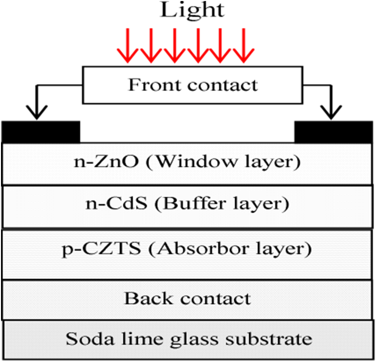
Figure 1: Schematic structure of ZnO/CdS/CZTS solar cell used in AMPS-1D simulation
The current research work emphasizes the investigation of front and back contact barrier heights effects on cell performance. The front and back contacts barrier heights
where
The physical parameters the like band gap (Eg), electron affinity (χe), relatively electric permittivity (εr), effective density of states in the conduction and valence band (Nc and Nv), electron and hole mobilities (µe and µp) and electron and hole densities (n and p) of the ZnO, CdS and CZTS layers used for simulations were obtained from the literature [17,18], and are summarized in Table 1. All the properties of the window and the buffer layers remained unchanged, while the optical coefficient
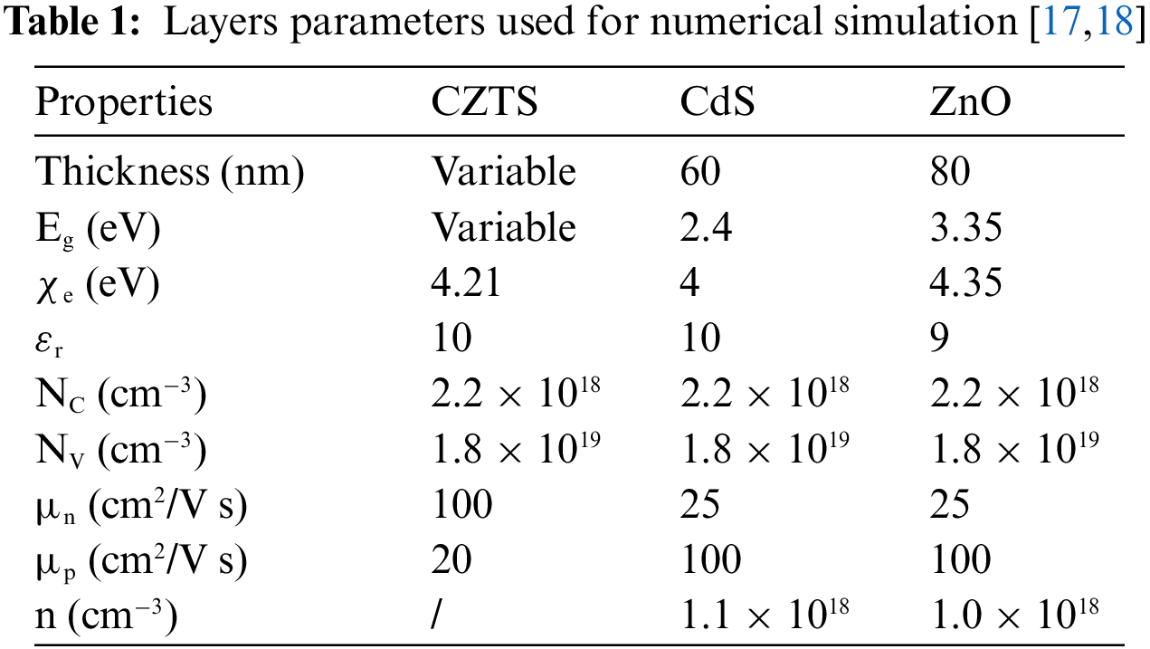
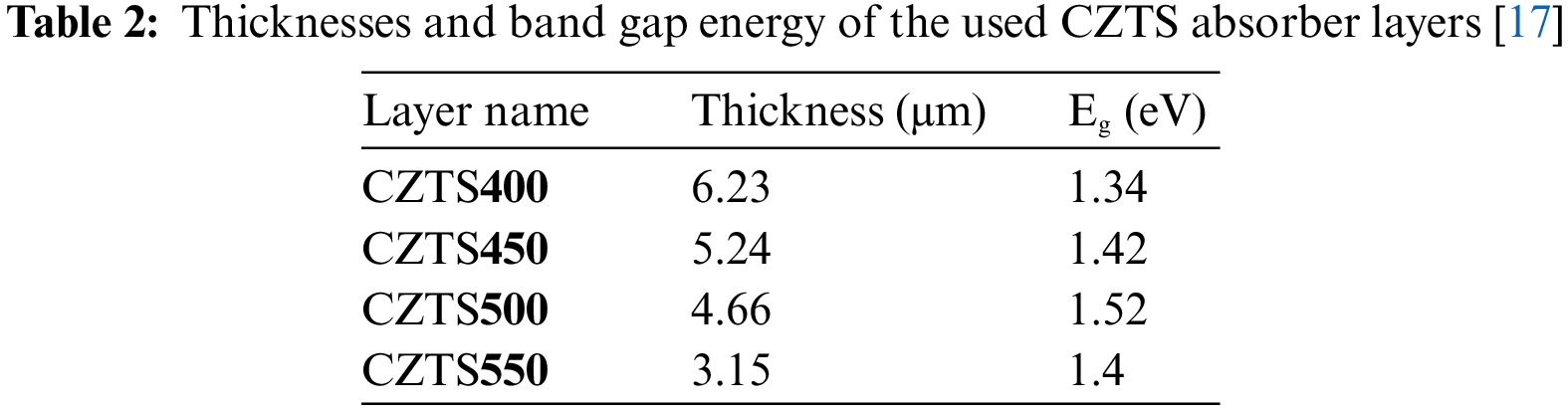
The four CZTS layers named CZTS400, CZTS450, CZTS500, and CZTS550 were produced by a one-step electrodeposition method followed, respectively, by sulfurization at 400°C, 450°C, 500°C, and 550°C. The layer thicknesses and its band gap energy are reported in Table 2 [17].
For simulations, we used the lifetime mode. The device performances were evaluated under AM1.5 illumination spectra, with P = 1000 W/m2 and the cell workting temperature was taken as room temperature (300°K).
The schematic energy band diagram of the (ZnO/CdS/CZTS550) cell under thermodynamic equilibrium conditions is shown in Fig. 2. The barriers created in the conduction and valence bands in CZTS/CdS and CdS/ZnO interfaces are due to the differences between the CZTS, CdS and ZnO electron affinities as well as the difference between their band gap energies. The conduction band offset
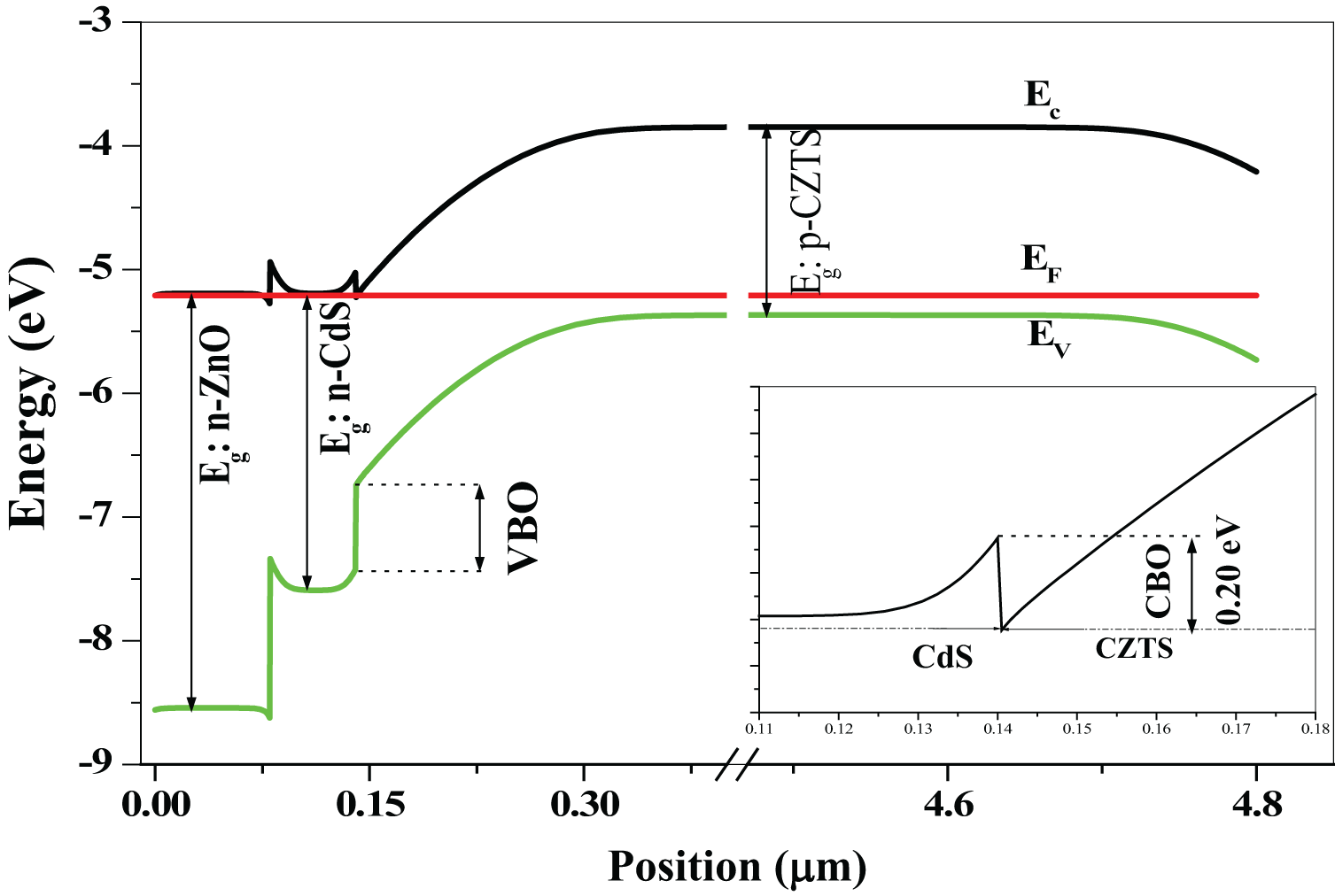
Figure 2: The schematic energy-band diagram of the optimal ZnO/CdS/CZTS550 cell under illumination at thermodynamic equilibrium
The obtained values are 0.21 and −0.35 eV (−0.85 and −1.3 eV). The conduction band offset (CBO) of the CdS/CZTS550 heterojunction was found to be spike-like with +0.21 eV. Therefore, the CBO barrier proposes a structure that does not prevent the collection of photogenerated carriers since it is positive and lower than the maximum value of 0.4 eV [19].
The solar cell performance parameters Voc, FF, η and JSC were determined from the light J (V) characteristics, and they are shown as a function of the back and front contacts barrier height for the different cells ZnO/CdS: CZTS400, CZTS450, CZTS500 and CZT550.
In this section, we display the effect of the front contact barrier height on the physical parameters of various CZTS solar cells.
The chosen metals as the front contact are ITO, FTO and TiO2 and their barrier heights at the ZnO layer vary from 0.01 to 0.77 eV [21–24].
The variations of JSC and VOC as a function of the front contact barrier height are depicted in Figs. 3a and 3b. For each CZTS cell, JSC is unaffected by the front contact barrier height, and it is almost constant (around 29.3 mA cm−2) for CZTS400, CZTS450, and CZTS550 cells, with a slightly high value for CZTS550 (Fig. 3a). This slight increase for the CZTS550 cell is due to the high absorption coefficient of the CZTS absorber layer [17].
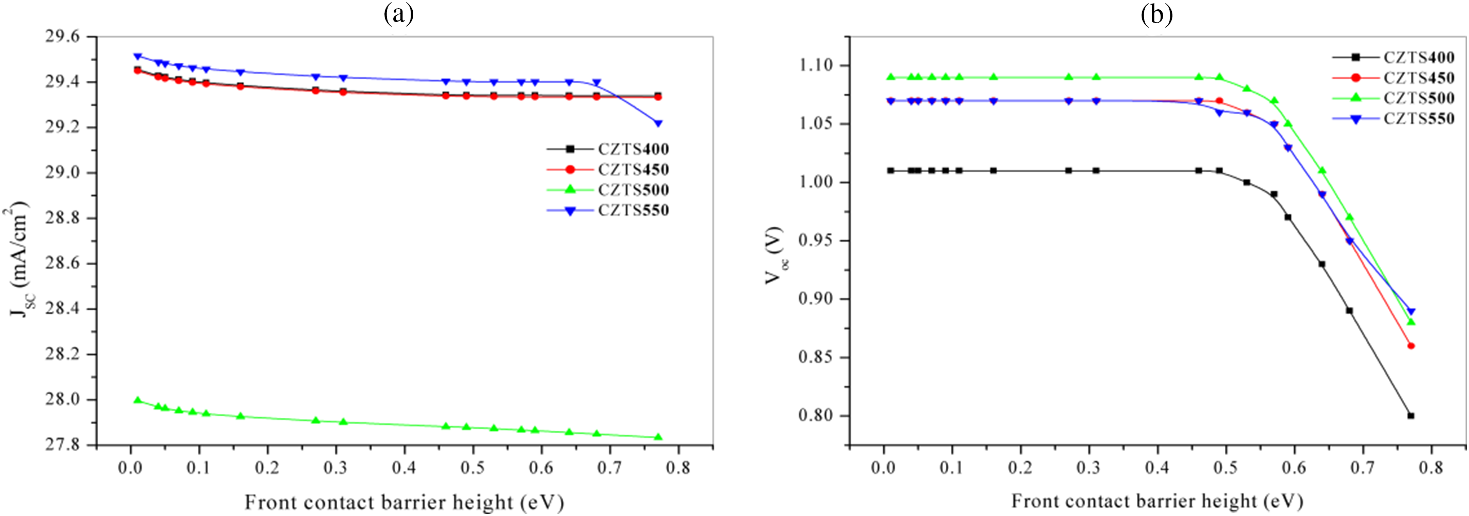
Figure 3: Variation of, (a): short circuit current density JSC and (b): open circuit voltage VOC vs. front contact barrier heights
However, a low short-circuit current density of about 27.8 mA cm−2 was observed in CZTS500 cells. This was due to the relatively high gap energy value of the CZTS absorber layer of this film (1.52 eV) compared to the other films and the alignment of the band edge of the back contact metal with the CZTS layer. We also noted that for wavelengths greater than 700 nm, the CZTS500 film had the highest optical transmittance and, therefore, the lowest absorbance [17]; this reduced the generation rate of electron-hole pairs limiting thereby the short-circuit current density [25]. Atowar Rahman presented in his work [26] the effect of the thickness of the CZTS absorber layer (varying from 1 to 5 μm) on the performance of solar cells. He reported that while VOC was not affected by the thickness of the CZTS layer, JSC varied between 28.94 and 32 mA cm−2, increasing up to a thickness of 3.5 μm, then saturating.
Concerning the open circuit voltage VOC shown in Fig. 3b, it takes a constant value for barrier height less than 0.49 eV, namely: 1.01 V for CZTS400, 1.09 V for CZTS500 and the same value of 1.07 V for CZTS450 and CZTS550. For barrier height greater than 0.49 eV, VOC decrease linearly to reach the low value 0.8 V at 0.8 eV. At the Metal/CZTS junction, a Schottky barrier is built due to an imbalance between the work function of the metal and the electron affinity in CZTS layers. This barrier prevents the carrier transportation to the metal electrode and reduces the VOC [27].
The dependence of the cell efficiency η and the fill factor FF for each CZTS cell on the front contact barrier height is depicted in Figs. 4a and 4b.
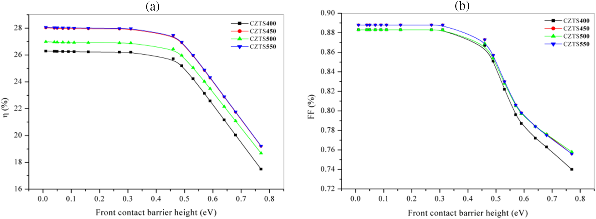
Figure 4: Variation of, (a): conversion efficiency η and (b): fill factor FF vs. front contact barrier heights
For barrier heights lower than 0.31 eV, the efficiency is independent of the front contact barrier height, but it depends on the properties of the CZTS layer, i.e., its band gap energy, thickness, and absorption coefficient. The CZTS550 cell has a maximum efficiency of 28.08% and the CZTS400 cell has a minimum efficiency of 26.2% (Fig. 4a).
In the second region (barrier heights above 0.31 eV), the power efficiency decreases rapidly to reach a minimum value of 18.6%.
Fig. 4b shows that the fill factor is not influenced by the properties of the CZTS layer and remains constant for barrier heights below 0.46 eV. It then decreases rapidly at lower values.
Among the most interesting properties of the Metal-Semiconductor interface includes its Schottky barrier height. The electronic transport, through the Metal-Semiconductor interface, is controlled by the Schottky barrier height, and thus, it is of major importance to the successful operation of any semiconductor device [28].
Increasing the front contact barrier height leads to an increase in the Schottky barrier, and consequently, reduces the quality of the front contact (non-ideal ohmic contact). The non-ohmic Schottky contact barrier could introduce additional interface resistance which increases the series resistance of the device [29].
Geuddim et al. reported a very close trend of the variation of the performance using a Cu2ZnSnS4 absorber by SCAPS-1D simulator [30], which is in good agreement with our work.
The open circuit voltage, efficiency, and short-current density have similar paces; this behavior has already been reported by Qiu et al. [31], Feldmann et al. [32] and Zhao et al. [33].
Figs. 5a and 5b show the dependence of η, JSC, and VOC on the energy band gap of the CZTS layer. We found that the efficiency increased from 26.21% to 27.98% (for CZTS550) when Eg increased from 1.34 to 1.42 eV. This increase was due to the increase in VOC. Nevertheless, for Eg above 1.42 eV, we observed a decrease in efficiency due to the decrease in JSC. We also found that JSC was almost constant in the first region
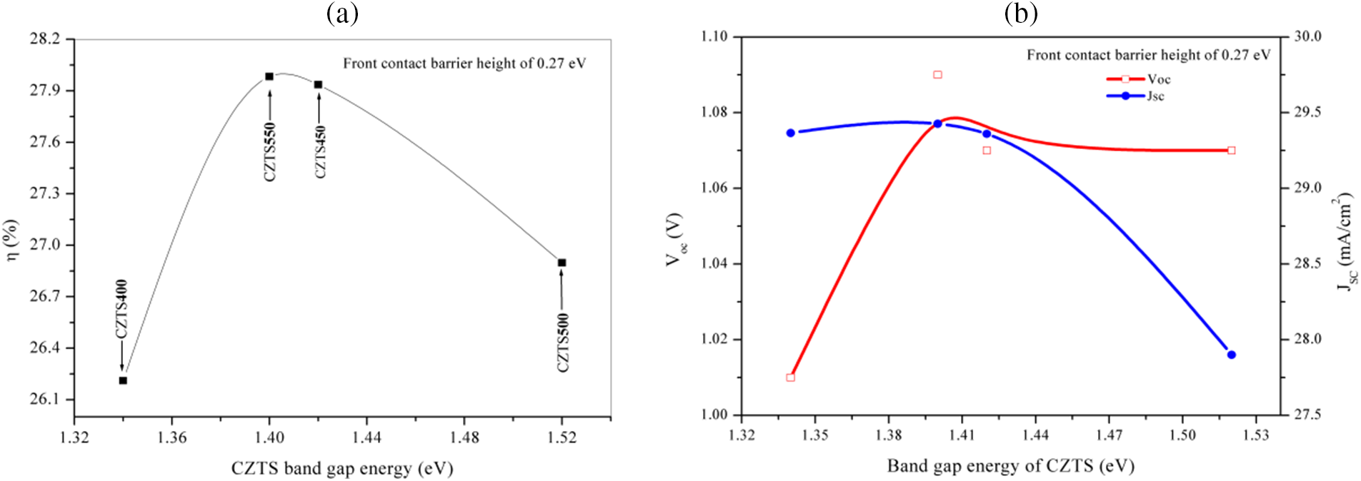
Figure 5: Variation of, (a): the conversion efficiency η and (b): the open circuit voltage VOC and short current density JSC vs. the band gap energy of CZTS for a front contact barrier height of 0.27 eV
The ZnO/CdS/CZTS550 cell performance parameters as η, JSC, and VOC mark the highest record because the CZTS550 absorber layer has an optimal thickness of
Atowar Rahman studied the effect of the thickness of the CZTS absorber layer on the performance of the cell with SnS/CZTS/TiO2/ITO structure. This study revealed that a relatively thicker absorber layer (4 microns) showed a maximum efficiency of ≈31% [26].
In this section, we show the effect of the back contact barrier height on the physical parameters of various CZTS solar cells. The metals selected as the back contact are Ag, Al, Os, Zn, Mo, Co, W, Ni, Au, Pt, and Re. Their barrier height varies from 0.5 to 1.55 eV [34,35].
A stable back contact that is not significantly rectifying is essential for good performance and long-term stability of CdS/CZTS solar cells; therefore, the choice of the back contact material has a high impact on the cell performance because the major differences in thin cells compared to the thicker ones is that the absorber/back contact interface is now located closer to the p–n junction [36].
Figs. 6a and 6b show the short circuit current density and open circuit voltage as function of the back contact barrier height for different CZTS thin film solar cells, respectively. We observed that for the barrier of less than 1.26 eV, the JSC remains constant; i.e., about 26 mA cm−2, and is it not influenced by the barrier height. However, it is observed that the short circuit current density increases rapidly up to 29.6 mA cm−2 for higher barrier heights. From Fig. 6b, it can be observed that the VOC is not affected by the properties of CZTS layer properties. However, for barrier heights lower than 1.03 eV, open circuit voltage was observed to increase linearly from 0.5 to 0.97 V, and become stable in the range 1.03 to 1.55 eV. The curves of the efficiency and the fill factor for each CZTS cell as a function of back contact barrier height are shown in Figs. 7a and 7b. From Fig. 7a, we can distinguish three stages. In the first stage; the barrier height is below 1.01 eV and in the third region; the barrier height is greater than 1.39 eV, the efficiency increases linearly with the barrier height and its maximum value is equal to 28.08% for CZTS450 and CZTS550. This increase in efficiency were achieved by changing the back contact metal work function.

Figure 6: Variation of, (a): short circuit current density Jsc and (b): open circuit voltage Voc vs. back contact barrier height
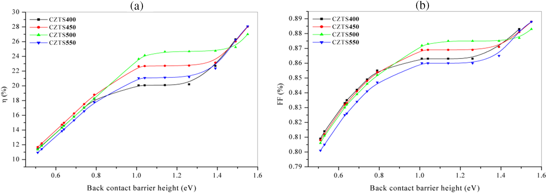
Figure 7: Variation of, (a): conversion efficiency η and (b): fill factor FF vs. back contact barrier height
In the second region, between 1.01 and 1.39 eV, the efficiency remains constant and is slightly dependent on the CZTS layer, especially its band gap energy. Efficiency and open-circuit voltage were observed to increase linearly with the band gap energy of CZTS (Figs. 8a and 8b).

Figure 8: Variation of the conversion efficiency η (a) and open circuit-voltage VOC (b) vs. the band gap energy of CZTS for a back contact barrier height of 1.14 eV
For Eg ranging from 1.34 to 1.52 eV, η and VOC vary from 20.9% to 24.63% and from 0.89 to 1.07 V, respectively. The value of the correlation coefficient
For all CZTS absorber layers, the electrical parameters increase as a function of the back contact barrier height and reach a maximum value at a barrier height of 1.55 eV owing to the increase in the charge carrier density generated by photon irradiation. The recombination of charge carriers is the most important limiting factor of the output power of solar cells. The recombination at the metallic contacts is highly dependent on the work function of the metal and the alignment of the energy bands of the metal and the absorber layers.
Atowar Rahman demonstrated that the higher recombination at the back contact of solar cells is the consequence of the greater band bending at the back contact [26]. Gong et al. improved the efficiency of CZTS/CdS/ZnO solar cells (11%) by heat treatments. The heat treatments lead to the reduction of non-radiative recombination by the formation of new secondary phases and the alignment of the band edge of the CZTS absorber layer and the metal [7].
Results show that creating a Schottky barrier with a large back-contact barrier height reduces the recombination rate of electrons and holes [38,39], leading to improved device efficiency.
Therefore the creating of the Schottky barrier back to a very low carrier density for high Eg CZTS results in the formation of a Schottky barrier or the presence of secondary phases that can act as a charge blocking layer at the back contact interface [29].
Moreover, with increasing metal work function, the barrier height for the majority of charge carriers (holes) at the back contact interface decreases improving the device performance [26]. Consequently, the higher metal work at the back contact reduces the recombination rate of electrons and holes which leads to an increase in the overall performance of the solar cells.
Toura et al. studied the effect of three back contacts ITO, FTO, and Mo on the performance of the CZTS/CdS/ZnO cell. They found that with Mo as a back contact, the cell has the best performance [40].
In summary, the AMPS-1D simulation program was used to study the effect of CZTS as an absorber layer; the front and the back contact barrier heights on the photovoltaic parameters of four ZnO/CdS/CZTS solar cells. We have found that for front contact barrier heights lower than 0.31 eV, the efficiency, fill factor and the open circuit voltage are almost constant. A maximum efficiency of 28.08% is obtained for CZTS450 and CZTS550. For the barrier height above 0.31 eV, the power efficiency for all cells decreases rapidly to reach a minimum value of 18.6%. The short current density is not affected by the front contact barrier height and it is minimum for CZTS500 cell.
The CZTS cells parameters are observed to be strongly influenced by the back contact material. The VOC, FF and η have a similar pace and increases with an increase in the front contact barrier height. The photovoltaic performances parameters, i.e., VOC, FF, JSC and η of the CZTS550 have reached their maximum values respectively, i.e., 1.07 V, 0.88, 29.5 mA cm−2 and 28.08% for the back contact barrier height of 1.55 eV.
Acknowledgement: The authors would like to acknowledge Prof. S. Fonash of the Pennsylvania State University for the Development of the AMPS-1D Simulator.
Funding Statement: The authors received no specific funding for this study.
Conflicts of Interest: The authors declare that they have no conflicts of interest to report regarding the present study.
References
1. Katagiri, H., Jimbo, K., Maw, W. S., Oishi, K., Yamazaki, M. et al. (2009). Development of CZTS-based thin film solar cells. Thin Solid Films, 517(7), 2455–2460. [Google Scholar]
2. Shadrokh, Z., Eshghi, H., Yazdani, A. (2015). Investigating the effects of temperature and metal ion ratio on physical and optical properties of Cu2ZnSnS4 nanoparticles and thin films. Materials Science in Semiconductor Processing, 40, 752–758. [Google Scholar]
3. Rao, M. C., Basha, S. K. S. (2018). RETRACTED: Structural and electrical properties of CZTS thin films by electrodeposition. Results in Physics, 9, 996–1006. [Google Scholar]
4. Gong, Y., Zhu, Q., Li, B., Wang, S., Duan, B. et al. (2022). Elemental de-mixing-induced epitaxial kesterite/CdS interface enabling 13%-efficiency kesterite solar cells. Nature Energy, 10, 966–977. [Google Scholar]
5. Kim, C., Hong, S. (2019). Relationship between residual strain and band gap of Cu2ZnSnS4 thin films grown by pre-sulfurized precursor. Molecular Crystals and Liquid Crystals, 678(1), 70–76. [Google Scholar]
6. Hoppe, H., Sariciftci, N. S. (2004). Organic solar cells: An overview. Journal of Materials Research, 19(7), 1924–1945. [Google Scholar]
7. Yan, C., Huang, J., Sun, K., Johnston, S., Zhang, Y. et al. (2018). Cu2ZnSnS4 solar cells with over 10% power conversion efficiency enabled by heterojunction heat treatment. Nature Energy, 3, 764–772. [Google Scholar]
8. Bashahu, M., Habyarimana, A. (1995). Review and test of methods for determination of the solar cell series resistance. Renewable Energy, 6(2), 129–138. [Google Scholar]
9. Tersoff, J. (1985). Schottky barriers and semiconductor band structures. Physical Review B, 32(10), 6968. [Google Scholar]
10. Tersoff, J. (1984). Schottky barrier heights and the continuum of gap states. Physical Review Letters, 52(6), 465. [Google Scholar]
11. Rubinelli, F. A., Arch, J. K., Fonas, S. J. (1992). Effect of contact barrier heights on a-Si: H p-i-n detector and solar-cell performance. Journal of Applied Physics, 72(4), 1621–1630. [Google Scholar]
12. Arch, J., Hou, J., Howland, W., McElheny, P., Moquin, A. et al. (1997). A manual for AMPS-1D BETA version 1.00. The Pennsylvania State University, Pennsylvania. [Google Scholar]
13. Burgelman, M., Verschraegen, J., Degrave, S., Nollet, P. (2004). Modeling thin film PV devices. Progress in Photovoltaics: Research and Applications, 12(2–3), 143–153. [Google Scholar]
14. Willars-Rodríguez, F. J., Chavez-Urbiola, I. R., Ramirez-Bon, R., Vorobiev, P., Vorobiev, Y. V. (2020). Effects of aluminum doping in CdS thin films prepared by CBD and the performance on Schottky diodes TCO/CdS:Al/C. Journal of Alloys and Compounds, 817, 152740. [Google Scholar]
15. Ma, L., Ai, X., Wu, X. (2017). Effect of substrate and Zn doping on the structural, optical and electrical properties of CdS thin films prepared by CBD method. Journal of Alloys and Compounds, 691, 399–406. [Google Scholar]
16. Wahid, R. R. (2019). Design and simulation of CZTS solar cell with ZnxCd1-xS window layer by AMPS 1-D (Master Thesis). Department of Electrical and Electronic Engineering, Dhaka University, Bangladesh. [Google Scholar]
17. Boudaira, R., Meglali, O., Bouraiou, A., Attaf, N., Sedrati, C. et al. (2020). Optimization of sulphurization temperature for the production of single-phase CZTS kesterite layers synthesized by electrodeposition. Surface Engineering, 36(9), 1000–1011. [Google Scholar]
18. Chandrasekharan, R. (2012). Numerical modeling of tin-based absorber devices for cost-effective solar photovoltaics (Ph.D. Thesis). University of the Pennsylvania State, USA. [Google Scholar]
19. Li, J., Wei, M., Du, Q., Liu, W., Jiang, G. et al. (2013). The band alignment at CdS/Cu2ZnSnSe4 heterojunction interface. Surface and Interface Analysis, 45(2), 682–684. [Google Scholar]
20. Boudour, S., Bouchama, I., Bouarissa, N., Hadjab, M. (2019). A study of CdTe solar cells using Ga-doped MgxZn1-xO buffer/TCO layers: Simulation and performance analysis. Journal of Science: Advanced Materials and Devices, 4(1), 111–115. [Google Scholar]
21. Helander, M. G., Greiner, M. T., Wang, Z. B., Tang, W. M., Lu, Z. H. (2011). Work function of fluorine doped tin oxide. Journal of Vacuum Science & Technology A, 29(1), 011019. [Google Scholar]
22. Schlaf, R., Murata, H., Kafafi, Z. H. (2001). Work function measurements on indium tin oxide films. J. Electron Spectroscopy and Related Phenomena, 120(1–3), 149–154. [Google Scholar]
23. Riviere, J. C. (1966). The work function of gold. Applied Physics Letters, 8(7), 172. [Google Scholar]
24. Yang, Q., Hu, M., Guo, J., Ge, Z., Feng, J. (2018). Synthesis and enhanced photocatalytic performance of Ag/AgCl/TiO2 nanocomposites prepared by ion exchange method. Journal of Materiomics, 4(4), 402–411. [Google Scholar]
25. Khemiri, N., Chamekh, S., Kanzari, M. (2020). Properties of thermally evaporated CZTS thin films and numerical simulation of earth-abundant and non-toxic CZTS/Zn(S,O) based solar cells. Solar Energy, 207, 496–502. [Google Scholar]
26. Rahman, M. A. (2021). Enhancing the photovoltaic performance of Cd-free Cu2ZnSnS4 heterojunction solar cells using SnS HTL and TiO2 ETL. Solar Energy, 215, 64–76. [Google Scholar]
27. Ahmmed, M. S., Hao, X., Park, J., Hawkes, E. R., Green, M. A. (2015). Diode laser annealing of CZTS thin film solar cells. Proceedings of the IEEE 42nd Photovoltaic Specialist Conference (PVSC), pp. 1–5. New Orleans, LA, USA. [Google Scholar]
28. Touati, R., Trabelsi, I., Rabeh, M. B., Kanzari, M. (2017). Structural and electrical properties of the Al/p-Cu2ZnSnS4 thin film schottky diode. Journal of Materials Science: Materials in Electronics, 28, 5315–5322. [Google Scholar]
29. Tai, K. F., Gunawan, O., Kuwahara, M., Chen, S., Mhaisalkar, S. G. et al. (2016). Fill factor losses in Cu2ZnSn (SxSe1− x)4 solar cells: Insights from physical and electrical characterization of devices and exfoliated films. Advanced Energy Materials, 6(3), 1501609–1501610. [Google Scholar]
30. Gueddim, A., Bouarissa, N., Naas, A., Daoudi, F., Messikine, N. (2018). Characteristics and optimization of ZnO/CdS/CZTS photovoltaic solar cell. Applied Physics A, 124(2), 199–7. [Google Scholar]
31. Qiu, D., Duan, W., Lambertz, A., Bittkau, K., Steuter, P. et al. (2020). Front contact optimization for rear-junction SHJ solar cells with ultra-thin n-type nanocrystalline silicon oxide. Solar Energy Materials and Solar Cells, 209, 110471–110477. [Google Scholar]
32. Feldmann, F., Simon, M., Bivour, M., Reichel, C., Hermle, M. et al. (2014). Efficient carrier-selective p-and n-contacts for Si solar cells. Solar Energy Materials and Solar Cells, 131, 100–104. [Google Scholar]
33. Zhao, L., Zhou, C. L., Li, H., Diao, H. L., Wang, W. J. (2008). Role of the work function of transparent conductive oxide on the performance of amorphous/crystalline silicon heterojunction solar cells studied by computer simulation. Physica Status Solidi A—Application and Materials Science, 205(5), 1215–1221. [Google Scholar]
34. Patel, M., Ray, A. (2012). Enhancement of output performance of Cu2ZnSnS4 thin film solar cells—A numerical simulation approach and comparison to experiments. Physica B: Condensed Matter, 407(21), 4391–4397. [Google Scholar]
35. Michaelson, H. B. (1977). The work function of the elements and its periodicity. Journal of Applied Physics, 48(11), 4729–4733. [Google Scholar]
36. Matin, M. A., Aliyu, M. M., Quadery, A. H., Amin, N. (2010). Prospects of novel front and back contacts for high efficiency cadmium telluride thin film solar cells from numerical analysis. Solar Energy Materials and Solar Cells, 94(9), 1496–1500. [Google Scholar]
37. Zhao, W. H., Zhou, W. L., Miao, X. S. (2012). Numerical simulation of CZTS thin film solar cell. Proceedings of the 7th IEEE International Conference on Nano/Micro Engineered and Molecular Systems (NEMS), pp. 502–505. Kyoto, Japan. [Google Scholar]
38. Demtsu, S., Sites, J. (2006). Effect of back-contact barrier on thin-film CdTe solar cells. Thin Solid Films, 510(1–2), 320–324. [Google Scholar]
39. Hädrich, M., Heisler, C., Reislöhner, U., Kraft, C., Metzner, H. (2011). Back contact formation in thin cadmium telluride solar cells. Thin Solid Films, 519(21), 7156–7159. [Google Scholar]
40. Toura, H., Khattak, Y. H., Baig, F., Soucase, B. M., Touhami, M. E. (2019). Back contact effect on electrodeposited CZTS kesterite thin films experimental and numerical investigation. Solar Energy, 194, 932–938. [Google Scholar]
Cite This Article
 Copyright © 2023 The Author(s). Published by Tech Science Press.
This work is licensed under a Creative Commons Attribution 4.0 International License , which permits unrestricted use, distribution, and reproduction in any medium, provided the original work is properly cited.
 Downloads
 Citation Tools